Note : Les descriptions sont présentées dans la langue officielle dans laquelle elles ont été soumises.
21 64803
METHOD AND CIRCUIT FOR
DRIVING PICTURE DISPLAY DEVICES
BACKGROUND OF THE INVENTION
Field of the Invention
The present invention relates to a method for driving
a driving circuit such as a driver or the like used in a
display device with a dot matrix of pixels.
Description of the Prior Art
According to prior art, writing pictures to liquid
crystal pixels is performed with, for example, a liquid
crystal dis~lay device, by providing liquid crystal
display elements with TFT devices used as switching
devices for application of voltages to liquid crystal
pixels with a configuration where one TFT device is
used as one pixel, drain terminals of the TFT devices
are connected to electrodes for the liquid crystal
pixels and their gate terminals and source terminals
are arranged as lengthwise and lateral common terminals,
applying voltages for the respective pixels to their
source common terminals as picture signals and applying
voltages for continuity between sources and drains of
the TFT devices to their gate common terminals thereby-
applying ON-voltages to all the TFT devices connected
to the gate common terminals (usually for one horizontal
21 64803
_ - 2
line on the display screen) to establish continuity
between the sources and the drains.
FIG . 7 is a view of the configuration of a
conventional liquid crystal panel with TFT devices.
Liquid crystal display devices are driven by two types
- of driving elements designated as source driver and
gate driver, connected to the TFT devices. In the case
of liquid crystal panels with pixels 1280 dots wide by
1024 dots high as shown there, for displaying of input
signals of 1280 x 1024 resolution, for example, picture
data for each pixel is designed to be displayed with
a single dot of the liquid crystal panel, eventuaily
filling the 1280 x 1024 screen exactly.
On the other hand, in cases where the input signals
have a 640 x 400 resolution, each pixel of picture data
is magnified twice vertically and horizontally as shown
in FIG. 5 for displaying over four dots of the liquid
crystal panel, thus resulting in an enlarged display
using 1280 x 800 pixels of the liquid crystal panel as
the display screen. As described above, the resolution
of input signals is increased twice vertically and
horizontally for enlarged displaying so long as the
increased resolution does not exceed the number of
pixels of the liquid crystal panel. This also applies
to other input signals of resolution capable of being
increased by an integral multiple, and displaying is
21 64803
- 3
- performed with no more than the maximum integral multiple
of the resolution which does not exceed the number of
pixels of the liquid crystal panel used in either of
the vertical and the horizontal directions.
Picture display areas have a variety of resolutions
depending on the particular pieces of hardware and
software used. For example, in cases where input
signals have a 1024 x 768 resolution and this resolution
is magnified twice vertically and horizontally to 2048 x
1536 which exceeds the number of pixels of the liquid
crystal panel used, all the information of the input
signals cannot be displayed on such a liquid crystal
panel as shown in FIG. 7. Therefore, displaying is
performed with the original 1024 x 768 resolution, as
shown in FIG. 6. This naturally results in a display
at the center or another area of the liquid crystal
panel at a smaller size than the liquid crystal panel.
In this case, however, since the full liquid crystal
panel screen is not used, there is presented a problem
of, for example, a dark screen because of insufficient
use of light from the light source since an increased
area is shielded from light in cases where the liquid
crystal panel is used as a light crystal projector.
SUMMARY OF THE INVENTION
It is therefore an object of the invention to provide
21 64803
-
-- 4
a method and circuit for driving a picture display device
of a dot matrix type, which is capable of displaying pictures
with a better use of pixels of the picture display device,
regardless of the resolution of the picture display device.
According to the present invention, there is provided
a method for driving a picture display device with a dot
matrix of plxels to display pictures based on picture
signals of any given resolution with any desired number
of pixels using the display device, comprising: displaying
an identical picture signal of one horizontal scanning
period in one or more lines each and varying the vertical
displaying magnification factor for the picture signal by
periodically varying the number of lines which display
the identical signal.
c
BRIEF DESCRIPTION OF THE DRAWINGS
Other objects, features and advantages of the present
invention will become more apparent when the following
description is read in conjunction with the accompanying
drawings, wherein:
FIG. 1 is a view illustrative of the configuration
of an embodiment according to the present invention;
FIG. 2 is a view illustrative of the embodiment
according to the present invention;
FIG. 3 is a view illustrative of an instance of
displaying according to the embodiment of the present
invention;
- 21 64803
FIG. 4 is a view illustrative of a drive timing
chart for a liquid crystal driver IC which realizes the
embodiment according to the present invention;
FIG. 5 is an instance of writing to liquid crystals
according to the prior art;
FIG. 6 is an instance of displaying of a picture
according to the prior arti
FIG. 7 is a view illustrative of the configuration
of a conventional liquid crystal panel;
FIG. 8 is a view illustrative of the configuration
of the representatlve gate driver,
FIG. 9 is a view illustrative of an embodiment of
a timing control circuit according to the present
invention; and
FIG. 10 is an operation timing chart for the timing
oontrol circuit shown in FIG. 9.
DETAILED DESCRIPTION OF THE PREFERRED EMBODIMENTS
First, an embodiment of the present invention will
be explained with reference to a case where a TFT active
matrix liquid crystal display is used as a picture display
device with a dot matrix of pixels.
FIG. 1 is a view illustrative of the configuration
of an embodiment according to the present invention,
FIG. 2 is a view illustrative of the operation of the
embodiment of the present invention, and FIG. 3 is a view
~ - 6 - 2164803
illustrative of an instance of displaying a picture with
the embodiment according to the present invention. In
addition, FIG. 4 is a view illustrative of an instance
of the drive timing chart of a liquid crystal driver IC
which realizes the embodiment according to the present
invention.
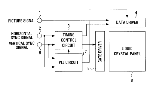
In FIG. 1, 1 denotes a picture signals are input
terminal through which picture signals are inputted to
a data driver 4. In addition, 2 denotes a synchronizing
signal input terminal through which, for example,
horizontal synchronizing signals and vertical synchronizing
signals are inputted. 3 denotes a timing control circuit
or a circuit for supplying a variety of timing pulses or
clocks, etc. to the data driver 4 and a gate driver 5 in
order to display input picture signals on a liqui-d crystal
panel. Also, 7 denotes a PIL circuit and 8 is the liquid
crystal panel.
The present invention relates to a liquid crystal
panel driving circuit which is effective for displaying
input signals of lower resolution then the number of
pixels of the liquid crystal panel used for displaying
images; for example, it is a liquid crystal panel driving
circuit which makes a better use of pixels of a liquid
crystal panel display in cases where input signals of
1020 x 768 resolution are being displayed on a liquid
crystal panel with resolution 1280 pixels wide by 1024
21 64803
pixels high. The state of a picture displayed according
to the present invention is such one as illustrated in
FIG. 3.
A characteristic aspect of the present invention
resides in a method for loading picture data into
liquid crystal pixels, as shown in FIG. 2, which is
a characteristic method for driving the gate driver 5
mainly vertically. First, the case will be described
where pictures of input signals of 1024 x 768 resolution
are being displayed through a better use of the screen
of a liquid crystal panel with resolution 1280 pixels
wide by 768 pixels high. Assuming that the pictures are
magnified at an identical ratio vertically and horizontally,
the resolution becomes 1280 x 960 when the ratio is 1.25
times in both the vertical and the horizontal directions,
and this 1.25-times magnification allows better use of
the pixels of the used liquid crystal panel for enlarged
display of pictures of input signals. The process of the
1.25-times vertical magnification is actually accomplished
by loading every four lines of picture data into five
lines of the liquid crystal panel. More specifically,
one of the four lines of picture data is loaded into
two lines of the liquid crystal panel, and the remaining
three lines of picture data is loaded into three lines
of the liquid crystal panel, respectively. A chart
illustrative of drive timing by a gate driver IC at this
~_ - 8 - 2164~03
- point in time is as shown in FIG. 4. Here, the data
driver for guiding picture signals to the liquid crystal
pixels are designed to sample and hold each line of the
picture signals for outputting to the liquid crystal
pixels. The configuration of a representative gate
driver is illustrated in FIG. 8.
As a brief explanation with reference to FIG. 4,
when the picture data is for scanning line 1, timing is
provided to output gate pulses of the first line and the
second line of the gate driver IC. Subsequently, when
the picture~data is for scanning lines 2 through 4, pulses
of the third lines through fifth line of the gate driver
IC are generated in succession. With these timing pulses,
loading of each four lines of picture data into five lines
of the liquid crystal panel is repeated until a total of
768 vertical lines of picture data is loaded into 960 lines
of the liquid crystal panel to accomplish a 1.25-times
vertical magnification. On the other hand, in the
horizontal direction, for example, in cases where the
picture signals are digitized, the sampling clocks are
increased to 1.25 times in synchronization with the
vertical magnification/reduction factor, and the number
of samples of the picture data is increased from 1024
dots to 1280 dots or 1.25 times for the horizontal
magnification.
In this connection, FIG. 9 illustrates in instance
2~ 6~Q3
g
of the configuration of the timing control circuit 3 for
generation of the gate driver IC shift clocks shown in
the timing chart of FIG. 4, while FIG. 10 illustrates
timing charts for the respective signals. For a brief
explanation with reference to FIG. 9, first, input clocks
22 and half clocks 23 generated by dividing the clocks 22
into halves by a divider 15 are inputted to A and B of
a selector 17, respectively. The function of this
selector 17 is designed to output the A input to Y when
the selector terminal S is at a low level and the B input
to Y when the selector terminal S is at a high level.
The counter 16 is designed so as to count up upon reverse
clocks of the input clocks 22 and to input an output 24
of the counter 16 to A of each of two comparators 18
and 19.
On the other hand, appropriate data depending on the
magnification factor at that time is inputted to B of
each of the comparator 18 and the comparator 19; in this
embodiment it is intended that "2" is inputted to B of
the comparator 18, whiie "7" is inputted to B of the
comparator 19. In other words, the output 25 of the
comparator 18 is LOW when the output 24 of the counter
16 is smaller than 2 and HIGH when the output 24 of the
counter 16 is 2 or greater, whereas the output 26 of the
comparator 19 is HIGH when the output 24 of the counter
16 is 7 and LOW otherwise. The output 25 of the
`-- - lO - 2164803
comparator 18 is connected to the selector terminal S of
the selector 17, while the output 26 of the comparator 19
is connected to the reset terminal of the counter 16.
Here, the counter 16 is designed to be such a counter as
to be reset in synchronization with a clock when the reset
terminal is HIGH. The operation of the above-explained
timing control circuit shown in FIG. 9 is illustrated by
the timing chart shown in FIG. 10 which demonstrates the
successful operation of the present invention by realizing
such a gate driver IC drive timing chart as shown in
FIG. 4.
Even drivers which have different configurations and
different modes of operation from the gate driver and the
data driver described above may accomplish the desired
function so long as each single line of picture data-may
be loaded into a plurality of lines of the panel and the
number of lines for loading is controllable within one
frame. It will be easily understood that the effect of
the present invention may be produced not only by timing
operation with a driver IC as shown in FIG. 4 which is
means for loading each one line of picture data into a
plurality of lines of the panel without using any storage
element such as a memory, but also by using a storage
element such as a memory.
In the same manner as the one described above, the
magnification of display may be varied as desired for
21 64803
-- 11 --
other magnification factors as well by controlling the
number of writable lines (controlling the drive timing
with the gate driver IC) with respect to the vertical
direction and by varying the sampling clocks with respect
to the horizontal direction.
In addition, the present invention may be applied
to display devices with a dot matrix of pixels, and
an entirely identical effect to that of the present
invention may be produced in any mode of displaying
in which picture data is distributed to the respective
pixels for displaying so long as the distribution of
picture signals to the respective pixels for displaying
- may be achieved in the same manner as in the embodiment
described above. In other words, the present invention
may also be applied to display devices other than the
TFT active matrix liquid crystal display explained in
the above embodiment, for example, display devices with
a dot matrix of light-emitting elements such as LEDs
or plasma displays.
As explained above, with picture display devices
with a dot matrix of pixels, the present invention
allows better use of displayable areas of such picture
display devices by writing and displaying of the m~ximum
picture data possible over the entire displayable areas
of the picture display devices, which is achieved by a
technique for displaying each picture over an any desired
21 64803
- 12 -
number of pixels in cases where picture signals of any
given resolution are being displayed on the picture
display devices used.