Note : Les descriptions sont présentées dans la langue officielle dans laquelle elles ont été soumises.
,....
2176772
-1-
CONNECTING BLOCK PROTECTOR DEVICE
Background of the Invention
This invention relates to current and/or voltage protectors for inserting into
a
connecting block.
Connecting blocks are used in telecommunications systems for providing
electrical
connection at central offices and other locations between incoming and
outgoing cables and
to provide a cross-connection capability. Such connecting blocks also normally
include
voltage and current limiting protection devices to prevent damage to the
circuits connected to
the block. (See, e.g., U.S. Patent. Nos. 4,171,857 and 4,283,103 issued to
Forberg et al.)
The protectors usually include a voltage surge protector element, such as a
gas tube,
current limiting devices, such as positive temperature coefficient (PTC)
resistors, a ground
electrode, and some form of thermal overload protection which short circuits
the protector to
ground in the event that any heat generated by the protector becomes
excessive. The elements
are typically mounted on a printed circuit board. (See, e.g., U.S. Patent. No.
5,299,088 issued
to Honl et al.) The thermal overload protection is usually triggered by the
melting of one or
more solder pellets which brings a ground contact into electrical contact with
the electrodes
of the surge element. (See also U.S. Patent. No. 5,248,953 issued to Honl and
U.S. Patent.
No. 4,642,723 issued to Achtnig et al.)
Such connectors perform satisfactorily. However, recently, connecting blocks
have
been proposed with short distances between adjacent contact pairs. (See, e.g.,
U.S. patent
application of Conorich et al., Ser. No. 08/442,862, filed May 17, 1995, and
assigned to the
present assignee.) Such short distances require smaller protectors, which are
difficult to
achieve considering all the elements needed for such a protector.
Summary of the Invention
The invention is a protector device including a housing and adapted for
insertion in a
connecting block. The device comprises a voltage surge protector element
having a pair of
biasing electrodes and a ground electrode mounted within a housing. The device
further
includes a ground connector comprising an elongated conductive member
electrically
contacting the ground electrode and having an end portion formed into a detent
which is
aligned with an opening in the housing so that the end portion is adapted to
receive and retain
.-.
2176772
-2-
a ground bar on the connecting block. The connector is insulated from the
biasing electrodes.
A fusible element is formed on the protector element and mounted with respect
to the ground
connector so that the ground connector will also contact the biasing
electrodes when the
fusible element melts due to the temperature of the protector element reaching
a
predetermined value.
In accordance with one aspect of the present invention there is provided a
protector
device adapted for insertion in a connecting block comprising: a housing; a
voltage surge
protector element mounted within the housing and having a pair of biasing
electrodes and a
ground electrode; a ground connector comprising an elongated conductive member
electrically contacting the ground electrode and having an end portion formed
into a detent
which is aligned with an opening in the housing so that the end portion is
adapted to receive
and retain a ground bar on the connecting block, the said connector being
insulated from the
biasing electrodes; and a fusible element formed on the protector element and
being mounted
with respect to the ground connector such that the ground connector will also
contact the
biasing electrodes when the fusible element melts due to the temperature of
the protector
element reaching a predetermined value.
In accordance with another aspect of the present invention there is provided a
protector device adapted for insertion in a connecting block comprising: a
housing; a voltage
surge protector element mounted within the housing and having a pair of
biasing electrodes
and a ground electrode; an essentially C-shaped conductive clamp mounted to
the surge
protector element so as to make mechanical and electrical contact to the
ground electrode; a
fusible insulating layer formed on the biasing electrodes so as to insulate
the biasing
electrodes from the clamp; and a ground connector having a portion
electrically and
mechanically contacting the clamp and having an end portion formed into a
detent which is
aligned with an opening in the housing so that the end portion is adapted to
receive and retain
a ground bar on the connecting block.
Brief Description of the Drawings
These and other features of the invention are delineated in detail in the
following
description.
FIG. 1 is a perspective view of a connecting block with a plurality of
protector devices
inserted therein;
x_
2176772
...-.
-2a-
FIG. 2 is a cross-sectional view of one of the modules of the connecting block
of FIG.
1 without a protector inserted therein;
FIG. 3 is a cross-sectional view of the same module with a protector device
inserted
therein;
FIG. 4 is a side, cross-sectional view of a protector device in accordance
with one
embodiment of the invention; and
FIG. 5 is a side, cross-sectional view of a protector device in accordance
with a further
embodiment of the invention.
It will be appreciated that, for purposes of illustration, these figures are
not necessarily
drawn to scale.
Detailed Description
FIGS. 1 and 2 illustrate one type of connecting block, 10, which may utilize
the
protector devices, e.g., 20, in accordance with the invention.
The connecting block, 10, includes a plurality of connector modules, e.g., 50,
which
are inserted into a hinged mounting bracket, 51. As illustrated in FIG. 2,
each module
includes an insulating housing having a rectangular-shaped body portion, 11,
with insulating
caps, 14 and 15, a portion of which define a top surface, 12, and bottom
surface, 13,
respectively. A row of insulation displacement contacts, e.g., 30, extends
through the top
surface, 12, and a row of insulation displacement contacts, e.g., 31, extends
through the
bottom surface, 13. Each contact, 30 and 31, includes an end portion, 32 and
33, protruding
through the surface, the end portions having an insulation-piercing slit, 34
and 35. Each end
portion, 32 and 33, is capable of receiving a wire, 60 and 61, for purposes of
providing
electrical connection thereto. Each contact also includes a stem portion, 42
and 43, which is
housed in the body portion, 11, and makes contact with a corresponding contact
in the other
row, desirably, at two points, 38 and 39, to electrically connect the wires,
60 and 61, coupled
to corresponding contacts, 30 and 31, in the two rows.
~:
2176772
-3-
The contact points, 38 and 39, are aligned with respective slots, 17 and
18, in the top and bottom surfaces, 12 and 13, to permit insertion of leads
from
protectors or other elements mounted on the top or bottom surfaces. For
example,
FIG. 1 shows a row of protector devices, 20, in accordance with the invention
mounted to the top surface of the block, while FIG. 3 illustrates a single
protector
device, 21, mounted to the bottom surface of the block. It will be noted that
the
protector, 21, is electrically connected to the stem portions of the two
contacts, 30
and 31, as well as to the two adjacent contacts (not shown) in the row by
means of a
lead, 40, which has its two major surfaces insulated from each other so that
current is
forced to flow through the protector device in the manner illustrated by the
arrows.
Further, the protector device is electrically coupled to a ground bar, 19 of
FIG. 2, on
the surface of the block so. that excess current and voltage can be diverrted
to ground.
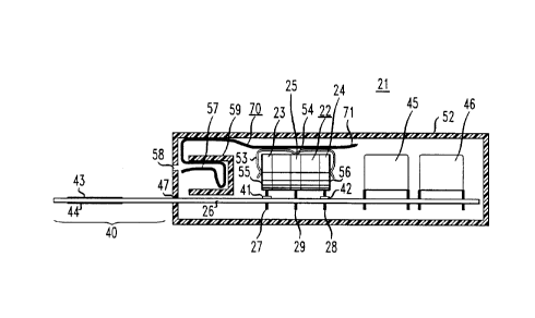
As illustrated in FIG. 4, the protector device, 21, in accordance with one
embodiment includes a voltage surge protector element, 22, such as a standard
gas
tube protector. The element, 22, includes a pair of biasing electrodes, 23 and
24, at
either end of the tube, and a ground electrode, 25, at the center. The tube is
through-hole mounted to a printed circuit board, 26, by soldering pins, 27-29,
connected to the tube electrodes, 23-25, respectively. The pins, 27 and 28,
connected to the biasing electrodes, 23 and 24, are electrically coupled to
conductive
pads, 41 and 42, on the circuit board so that the electrodes are electrically
coupled to
the contact pads, e.g., 43 or 44, on the lead portion, 40, which are on the
surface of
the circuit board, 26. The pin, 29, coupled to the ground electrode, 25,
however, is
electrically isolated from other components or conductive paths on the board.
The voltage surge protector element, 22, is electrically coupled to a pair
of positive temperature coefficient (PTC) resistors, 45 and 46, which are also
through-hole mounted by soldering to the printed circuit board, 26. The surge
protector element, 22, and PTC resistors, 45 and 46, are protected by an
insulating
housing, 52, such as plastic, which encloses those components and a portion of
the
board, 26. A portion, 40, of the board, 26, previously referred to as the lead
portion,
protrudes through an opening, 47, in the housing, 52, to permit insertion of
said lead
portion into the connecting block as illustrated in FIG. 3.
Attached to the surge protector element, 22, is a generally C-shaped
conductive clamp, 53. The center of the clamp, 53, includes a dimpled portion,
54,
which makes electrical and mechanical contact with the ground electrode, 25.
The
ends of the clamp are in mechanical contact with insulating fusible layers, 55
and 56,
which are deposited on the biasing electrodes, 23 and 24, respectively. The
2176172
-4-
insulating layers, 55 and 56, are preferably made of a material such as
Mylarc9,
which has a melting point of less than 260 degtrcs C with a thickness in the
range
0.025 to 0.076 mm. The clamp is attached to the element, 22, by spot welding.
Electrically coupled to the clamp, 53, is a ground connector, 70, which
can be a thin metallic sheet having approximately the same width as the
housing, 52.
For example, the connector, 70, can be made of beryllium-copper with a
thickness in
the range 0.25 to 0.5 mm. The sheet is shaped to form an arcuate portion, 71,
at one
end which mechanically contacts the clamp, 53, and is also wedged between the
clamp and the housing, 52. The other end of the sheet is shaped into a detent,
57,
which is aligned with an opening, 58, in the housing, 52, so that when the
lead, 40, is
inserted into the connecting block as shown in FIG. 3, the detent, 57, will
receive
and hold the ground bar, 19 of FIG. 2, with a "clicking" noise so that the
craftsperson
knows the protector device is fully inserted. The detent can be held in place
by an
essentially C-shaped projection, 59, which is attached to or integral with the
back
surface of the housing, 52. If desired, the detent can include a hole (not
shown) f~
receiving a dimpled portion in the ground bar ( 19 of FIG. 2)
During normal operation, current will be conducted in the direction
illustrated in FIG. 3 with the surge protector element, 22, being non-
conductive.
Excess current will be prevented by the changing resistance of the PTC
resistors in
accordance with known techniques. When the voltage appearing on the biasing
electrodes, 23 and 24, reaches a threshold value, the tube, 22, will conduct
current to
the ground electrode 25, through the clamp, 53, and the connector, 70, to the
ground
bar, 19, of the connecting block so that protection from voltage surges is
provided.
It will be appreciated that in the usual prooector device, excess voltage
would be
shunted through the ground pin, 29. However, applicants have discovered that
by
electrically isolating the ground pin and providing the ground path through
connector
70 instead, the circuit board, 26, can be made narrower (typically 6.1 mm) so
that the
device can fit within the connecting module, 50, having very narrow spaces
between
adjacent contacts.
Further, in the event of thermal overload, the insulating films, 55 and
56, will melt, thereby bringing the ends of the C-shaped clamp into mechanical
and
electrical contact with the biasing electrodes 23 and 24. Since the clamp is
coupled
to ground through the connector, 70, the entire device would be short
circuited,
preventing any thermal damage to the circuits coupled to the connecting block.
Since the connector, 70, acts to prevent both excess voltage and thermal
overload,
again, the protector device can be made smaller.
2176112
-5-
FIG. 5 illustrates an alternative embodiment where elements similar to
those in FIG. 4 have been similarly numbered. Here, the gas tube, 22, has been
replaced by a solid state voltage protector element, 80. In place of the
clamp, 53, is a
fusible solder pellet, 81, which is deposited on the ground electrode, 62, of
the
voltage protector element. Again, the pin, 63, coupled to the ground
electrode, 62, is
electrically isolated. In this embodiment, excess voltages will be shunted
through
the pellet and connector, 70, to the ground bar, 19, of the connecting block.
It will
be noted that the connector, 70, in this embodiment has two dimpled portions,
64
and 65, which are positioned above but spaced from the biasing electrodes, 66
and
67, respectively. In the event of thermal overload, the pellet, 81, will melt,
causing
the dimpled portions, 64 and 65 to electrically and mechanically contact their
respective biasing electrodes, 66 and 67, to short out the device through the
connector 70. Again, since the ground pin is isolated, and the connector, 70,
is used
for both voltage and thermal overload protection, the protector device can be
made
smaller.
s