Note : Les descriptions sont présentées dans la langue officielle dans laquelle elles ont été soumises.
WO 95/lU87 PCT/SE94/01189
21801~4
llTLE: COA~PO~ NT-MOD~E-A DAPrED
OSCILI,AT~G CIRCUIT AR~TG~MENT
TECHI~rCA~ FIELD
The present invention relates to an oscillating circuit arrangement that is
5 adapted for a component module, and specifically to the kind of oscillating
circuit arrangements that are adapted to produce signals with a high frequency
and small frequency span, such as frequencies andfor bit rates within, at least,the MHz or Mbit/s range and abo~e.
Oscillating circuit arrancements of this kind normally comprise an
10 amplifying circuit and the circuit that generates the oscillating signal, usually in
the fonn of an oscillating element, and more specifically an oscillating elelllent
~vith a pronollnced resonance ..ec1uencv, a ~o-called resonance element Qr
ccmpollent. ~ ith electric wirin.~J a!nd ComFetlcatillo net~!orl~s or eleme!~ts, such as
inductance elements as needed.
An oscillating circuit of this kind can preferably be useful as a separate
circuit arrangement to be able to generale a synchronizing signal in circuit
internal signal processing to one or seYeral signal processing units. rt can also
be used to generate clock pulses ~vithin a con~municatioll system, to tr~nsmit
inforlnation carrying signals ~here the pulses together with data signals can be20 transmitted from a signal trancmitting unit OlltO a transmission line or in a sigllal
receiving unit.
The in~ention is ~ased on the principle that in each case tlle oscillating
CilCUit arral~gel]lent iS to be supported by a carrier sul)strate fomling a component
nlodule \~;here the top la~ier ol .lle c~rrier sul~strate upllok3s the c!iscrete25 colnponellts of ~he oscillatina circuit arran ,enlellt an(l .Ill intearated circuit
arrangement. L
BACKGROUND ART
Oscillatina circuit arran~elllents of the kind that generate a signal with a
30 chosen high frequency of at least 100 MHz or Illore and with a small frequency
WO 95/18487 PCr/SE94/01189
- 218~16~
span are earlier known in se~eral different embodiments with regards to chose~
components such as oscillating ~lement, chosen circuit arrangement and
mechanical disposition. Such an oscillating circuit arrangement can be a part ofa phase-locked loop (PLL) system where the oscillating component or element
consists of a Yoltage-controlled oscillator (VCO). Oscillating circuit
arrangements \Yhere the oscillat;ng component consists of a surface acoustic ~/ave
(SAW) component are designated as VCSOs (~oltage-controlled SAW oscillators)
or VCSO systerns.
U.S. Patenls ~To 4,760 3~2 and No. 5,325,032 show and describe
10 examples of oscillating circuits wilh SAW-elements or -components. Other units
are shown and described in European patent publication Nos. EP 0 527 468;
EP 0 495 316; EP 0 217 713; and EP 0 241 236; Jap~n~se patent publication
No. JP-A- 2 207 601; and U.S. Patent No. 5,029,'767.
An additional oscillating circuit arrangell~ent o~ this k ind. ~YIlere the
1~ complete system or par;s of ti~e systelll can be integrated Oll one or several
recei~er circuits, is kno~n as a rre~uency-controlled SAW oscillator (FCSO) or
~CSO system.
Oscillating circuil arrangements can be used in both earlier mentioned
VCSO- and FCSO-syslems where a SAW-component is used and \vhere the
20 circuit arrangement is based upon a feedback of the frequency of the SA~-
componellt at the resonanc~ frequency of the filter.
Crystal controlled SA~ oscillators have also been described, where the
crystal, used as an oscillafing elemellt, is mounted in its o~vn oscillating unit,
adapted to generate the necessary reference frequency to the SA~-component
25 and its oscillator circuit
Arrallgelnents o~ [llis }~ir.d are base(l upcll the t;act tllat, at Lesorance, (he
SA~T~-filter component presents a phase shift of 90 bet~een the input and output
terminals. The phase-shifted output signal is fed back through an amplifier thatis phase-angle adjustable around the resonance frequency at a range of 60 to
30 120. The phase variatiolls and the amplifier can easily be operated by a control
wo 95/18487 PcI~lsEs4lollss
` - 21801G4
~oltage with these kind of oscillating circuit arrangements. One can thus achi~ve
an accurate frequency and frequency tuning around the resonance frequellcy of
the SAW-filter with the aid of such a control voltage.
A SAW-component is characterized by a very narrow frequency span,
5 ~ith typically a few-percent deviation, depending on the chosen type of SAW-
component, and a very pure frequency with well repressed subhannonics and
- harmonics. SAW-components ha~e proven suitable for very high oscillating
frequencies, frequencies from some tens of MHz to a number of GHz.
Current experience ~vith hlown voltage-controlled SAW-components used
10 as VCOs and VCSO-oscillators is tllat tllese components are, in terms of spatial
volume, very large compared to the component modules and/or standard
integrated c;rcuits typically used. The function of such an oscillating circuit
arran~ement requires that the S~-component, usually together ~vith
compensating r.et~orl s~ sucll as i!lductarce elemerlts, e lectric ~irin~ arld
15 alllplifiers as needed, is co~.~ered in sQme !cir.d of cashlg, such as ~ ceramic holdcr
~rith a metal cup, and is lhus very expens;ve, particularly since this casing,
because of the sensitivity of the SAW-component, often has to be evacuated and
airtight. This technique, and the space tllat is thereby needed, has resulted inthat oscillating circuit arranoements of this kind have only been brought to use in
20 more e.Yclusive circumstances tvhere tlle various functional requirements are so
higll, Ol where the number of units is so lo~v, that the cost is of secondary
importance.
For all the above-mentioned oscillating circuit arrangements, one can say
that tlle mecl~anical disposi[ion of such an oscillating circuit arrangemeslt
25 illdicates tll~t the oscillatillo compollent1 necessary compensating networks, sucll
as islductallce elements, electric ~virino, ampliliers and so osl, is coordis~ated in a
separate evacuated airtigllt metal or ceralllic Init ~ith a metal c~sing. Sucll a
unit is physically separated and side-oriented from the component module
pertaining to other functions such as those used in telecommunication and
30 associated selectors or other equipment Oscillating circuit arrangements of this
WO 95rl8487 PCT/SE94tO1189
`- ~180164
kind, mounted in such a unit, cover a surface of at least 20 x 20 mm if not
more.
The basic principles of the present in~ention do not directly depend on the
chosen resonance element, but in the following, a SAW-element or SAW-
5 component will exemplify one of several available, and at prèsent most suitable,resonance elements. It ~ ~ill be understood that surface transverse ~vave (ST~)
components and surface skimming bul~ wave (SSBW) components are intended
to be included in the expression "SAW-component".
To further clarify the earlier oscillating circuit arrangements with
10 frequency accuracy, a categor)~ called crystal-oscillators, using crystals asoscillating- or resonance-elemen~s, can be mentioned. A crystal oscillator of this
kind ~vorks in the range of some hundreds of ~IHz in its keynote, or fundamentalfr.quency, and up to a fe~v hulldreds of MI~z if one of the hannol~ics of the
cr~stal is used. Oscillating circuit arrangelllellts ~vith a crysral as a resonallce
1~ element are used as oscillators and voltage-controlled cr)~stal oscillators
(vcxos). Such oscillators are a~ailable as small hole mounted plastic caps and
as very small surface mounted multilayer ceramic (MLC) modules. Oscillating
circuit arrangements of this Icind are, cost-wise, relatively inexpensive, but they
ha~e more frequency- and phase-noise (in other words! stronger subhamlonics
20 and harmonics) than the SAW-component arrangemellts and can therefore not
produce a frequency with tlle same purity as the one produced by a SAW-
component.
Oscillatino circuit arrallgelllents used to generate si~Jnals ~ith frequenciesill the range of some hundreds of M~z to some GHz use quarter-~Yave
~5 resonators. These are based UpO:l a resonatol- comprisillg a conductor, madc out
of a specific material, ~vith a length that corresponds to a quarteL of the
~avelength of the resonance &equency.
Oscillatin~ circuit arrangements of the type DCSO (digital control SAW
oscillator) use an oscillator controlled by a digital signal. The oscillator is
30 generally a VCSO where the control ~oltage is generated by a digital-to-analog
wo 95/18487 PCT/SEg4l0ll8g
` - 218016~
(D/A) converter. By suppl~ing a digital comln~ntl to the DCSO, one can get the
desired controlled ~oltage out of the D/A-con~erter. The D/A-con~erter can
either give an output ~oltage as a function-of input data or it can be a
potentiometer controlled by a dioit~l signal to achie~e the desired control ~oltage.
A D/A converter or di_ital trim potentiometer can receive its information in
either parallel or serial forn-. They can obviously be equipped witll some kind of
memory so tl~at the oscillator c~.n be restarted at a predetermined frequency after,
for instance, a po~er failure.
SUMMARY OF THE Ll`~VENTrON
TECHN~CAL PROBLEMS
- Considering the hlown s~stems described abo~e, it should be regarded as
a technical problem to create the conditions where a separately cased oscillating
unit is no~ re~luirecl aild tO nUt ~OinpOllell;S be~OnJiil ;';J ail ~ ior Oll ~1~ compollel~i module n;eal;t for O.;Jer fUI;C;10nS COiltiO31ed l~y it,c oseilla;or cireui;.
A technical problenl resides in beina able to see the collsequences and
im~ortallce of limitillg the size znd number used of discrete cased components,
applied to the carrier substrate ~f the component module.
It is a technical problem ~o be able to create the circumstances needed to
apply discrete components to a carrier substrate and, for such components that
normally require airtight casino, to create circumstances so that an airtight casino
of the integrated circuits on dle carrier substrate is not required.
There is a technical prob!em to realize tlle advantages tllat reside in
co~erina only the reson~nce element in an airtight casing to form a discrete
?.~ component and applyin~ this ;o ~he carrier substra;e of the component module.
Considerilla the kno~vll s~stems described abo~e, it should be regarded as
tecl~nica1 problelll to create s~!ch circulllstances on a compone~llt module so that
a necessary SAW-component~ recessary matching nel~vorkst sucll as inductailce
elements, inteorated circuits, electric wirino and amplifiers (all of which earlier
- 30 ~vere coordinated in an evacu~ted airtight metal casing, physically separated and
Wo 95/18487 rcrlsEs4/ollss
` - 2180164
side-oriented from the con ponent module pertaining to other functions) can be-
applied to the component module.
There is also a technical problem in being able to create the circ~-ms~nces
on the component module necessary to carry the complete oscillating circuit
5 arrangement, achieving the requirements of a smaller spatial volume and a better
coordination between utilized components then earlier kno~Yn.
It is also a techllical problem to create, on a component module, the
circ1~-nst~n~es necessary to allow the used resonance element (for instance, a
SAW-component) and the two matching networks or elements (for inS~nr~
lO ind--ct~n~es) to be oriented ~ery close to each other and close to an integrated
circuit, compr;sing among other tllings n~ceSs~ry amplifiers, and to in this
malmer create an embodiment that provides electromagnetic protection and
electrical wiring with, for high fre~uencies, small parasitic capacitances.
There is also a tecl nical prol~lem in being able to reali~e the ad~antages
15 hl allo~Ying the compo11el1t module to include the functions neces~ary for a signal
receiving circuit to be a part of the earlier mentioned integrated circuit, among
other things.
Considering the kno~vn systems described abo~e, it must also be seen as a
qualified technical problem to be able to create the circumstances n~cess~ry to
20 allo~v the complete oscillating circuit arrangement to be coordinated within a
limited part of the surface of a module and to form on a surface area electrically
conductive surface sections from the c~rrier substrate or circuit card belonging to
the component module. Tllese surface sections are formed and distributed in a
ay that they can coact ~vitll the corresponding contact surfaces of a resonal1ceelement, for instance a SAW-component, in a firm and electrically conductive
mamler. An integrated circ-lit, co1llprisil1g the required signal amplifying circuit
an(l furtller signal amplifyill~ alldtor signal processing cirCuits"~is attache(i to the
surface area adjacent to the surface sections and resonance element. The contactsurfaces of the resonance element are connected to the contact surfaces of the
30 carrier substrate by bonding or the lilce. The contact surfaces of the integrated
WO 9S/18487 PCI'ISE94/01189
`2180164
circuit are connected to the contact surfaces of the carrier substrate by bonding
or the like.
It is a t~chniçal problem to realize the advanta_es of adapting the:
component module to be a signal receiver and to allow the signal amplifying
and/or signal processing circuit to be adapted to signal receiving and signal
processing.
There is also a technic~l problem in realizing the advantages of fomling
further electrically conductive surface sections, from the carrier substrate or
circuit card, on a surface area belonging to the component module, these further10 surface sections being formed and distributed in a way that they can coact ~v;th
the corresponding contact surfaces of respective irnpedance elements in a ~Inn
and electrically conductive mamler and being oriented adjacent to the surface
areas belonging to the resonance element.
It is a ~rthcr techn.cai probl~m ~ able to realize-the ad~artag.s cf
15 oricnting ~h~ r,ecessary il~pedqllce e!ements 2djacent to !l~e r~sonanc~ eleinent, ill
the form of a SAW-element. andlor to the integrated circuit or to mount the
integrated circuit, a SAW-component, and t\vo irmpedance elements as discrete
eleMents to the carrier substra~e adjacent each other with tl~e electrical wiring
implemented on one surface of the carrier substrate so that the SAW-component,
or the SAW-component ~vith t~vo impedance elements, is covered by an
20 evacuated airtight casing.
SOLUTION
~ Vith the intentiol of solvill<J one or more of the aforesaid technical
problems, the present invelltion provides ~n oscillating circuit arrangement that is
adapted to a component module allcl that can l~avc a fundalnental frequenc~
highel tllall 100 MHz. The oscillatino circuit ~rrangement is applicable to a
small component module and adaptable tO form a signal with a high frequency
and a narrow frequency range. The oscillating circuit arrangement comprises a
30 signal amplifying circuit, a signal generating circuit with an oscillating element,
WO 95/lU87 PCTISE94101189
` - 218016~
-8-
any necess~ry matching network such as needed induct~n-~es, and electrical
~viring.
With such a component-module-adapted oscillating circuit arrangement,
electrically conductive surface cections are folmed on a surface area of a carrier
substrate. These surface sections are formed and distributed in a way that they
can coact in a firm and electrically conductive marmer ~vith corresponding
contact surfaces of a resonance element. An integrated circuit, comprising the
- signal amplifying circuit and h~rther signal amplifying and/or signal processing
circuits, is attached to the surface area adjacent to the contact surfaces of the
10 matchillg net~vork and the resonance element. Tlle contact surfaces of the
resonance element are connected to Ihe contact surfaces of the carrier substrateby bonding or the like. The contact surfaces of the integrated circuit are
connected to tlle contact surfaces of the carrier substrate by bonding or the like.
In acco;dance ~ ith tl~ ention, the compon.ent m~u~ule may l~e adapte(l
15 ;o ~ signal receiver alld the ~ign21 amplilying an(i/or ci~l~al !)r~ ces~ing circuits
adapted to signal receiving or signal processing.
Further, on a surface area of tlle carrier substrate, four electrically
conductive surface sections are fonned and distributed in pairs in a way that one
pair can coact in a firlll and electrically conductive manner with corresponding20 colltact surfaces of a matchillg net~vork in the folm of an impedance element.
Thcse four surface sections are oriented adjacent and on each side of the surface
sections of the resonance element.
According to the invention, the integrated circuit, resonance element, and
matching network may be attached to the carrier substrate adjacent to each otheras discrete components, \Yith lhe electrical ~ iring implemented mail~ly on one
sur~ace of tl~e carrier substrate an(l at least the resonallce element co\~ered by an
evacuated alld airti~ht casin~ .~lso, the resonance elemcllt and the matchin~
net~vork can be covered by a ceramic and/or metallic evacuated and airtight
casing.
WO 95/18487 P~,ll;il!,g 1/01189
- 2180164
ADVA~TAGES
An important advantage afforded by a component-module-adapted.
oscillating circu;t arrangement in accordance with the present invention is that the
small surface on a component module covered by the oscillating circuit
S arrangement makes conslruction less expensive and power consumption lo~er.
By applying a resonance eleMent co~ered in an airtight cas;n~ as a Ulli~ to a
con~ponent module, a surface area is acquired that is \~ell adapted to other
components, ~vhere the integrated circuit used does not nPcess~rily have to be in.
an airtight environment.
BREF DESCRIPI`IO~ OF THE DRAWINGS
An exemplifying embodiment of an oscillating circuit arrangement
comprising features significant to tlle invention will no~v ~e described in more~er2il ~ h reference to Ih.e accomnallying ara~Ying~, in ~Yhich:
Fig. 1 is a higlllv scllematic figure oF a transmitting system for
inforlllation carrying si~nals, having a transmitting circuit and a receiving circuit,
botll comprising an osci]lating circuit arrangemenl accordillg to tile present
n~ention;
Fig. 2 illustrates tlle prirc3pal COllStl~CtiOn of an oscillating circuit
arrallgement;
Fig. 3 illustrates, in plan ~ie~, the necessary components, circuits and
electrical wiring of an oscillatina circuit arrangement on an elllarged component
module;
Fi~. ~ illustrates, in section vie~v, tlle coverillc~ of a SAW-componellt in a
ceramlc casmg; and
Fi~. ~ illus(rates, in plall vie\.~, tl~e casing accordillg tO FiV. ~i.
~.
DESCRIPT~O~ OF E~BODIMENTS AT PRESENT PREFERRED
Fig. 1 illustrates an information carrying signalling system, lla~ing a
trallslllitter "S", a recei~er "R', an(l a transmissioll line "TR" connected
WO 95/18487 PCI'ISE94/01189
'~180164
-10-
tllerebetween. Both transmitter "S" and receiver "R" require an oscillating
circuit arrangement "O" to f~lnction. The oscillating circuit arrangement is used
to generate clock pulses and to synchronize:received pulses of identical form and
adapted tO the same fundamental frequency.
Required cooperation between tr~n~mitt~r and receiver and their
respective oscillating circuit arrangements is known to the art and it is therefore
nnPcess~ry to further describe the same. Nevertheless, it shall be mentioned
that the pulsed digital data signals transmitted from transmitter "S" are clock-pulse related across the tran~ cion line "TR", and these are received in the
10 receiver"R".
A control voltage is generated by receiver circuits in the receiver "R",
and tlie control voltage is fed through conductor 22 to the oscillating circuit
arrallgement "O", ~vhich in t-urn feeds a clock signal, in the form of pulses, out
on conductor 30. Tllus? the oscillating circuit arrangemcnt "O" is a VCO.
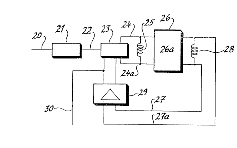
Fig. ~ illustrates a principal ~viring diagram OI an oscillating circuit
arrangement. A receiving circuit 21 detects signals Oll a conductor 20 and
presents, on its output conductor 22, a signal tb2t is used to control a first
amplifier 23 belonging to the oscillating circuit arrangement. Tlle receiving
circuit 21 can include a D/A converter. The signal on conductor 22 can l)e
20 adapted to control a time delay in the anlplifier 23, which has two output
conductors 24, 24a. A first matching net~ork, illustrated as an inductance 25,
and a resonance element ~6, ~hich may include a SAW-component 26a of an
earlier kno\ ~n construction, are coMected to the amplifier's output
conductors 24, ~4a. Two conductors 27, 27a from tlle resonance element 26 are
connected to each other throu~h a second matching net\~ork, illustrated as an
inductancc 2~, and further connected to a second alnplifier 29. Tll~ desired
frequency-stable signal generated is collected tllrough the conductor 30 and canbe used as a clock signal in the receiver circuits.
Tlle oscillating circuit arrangement IlOn, illustrated in Fig. 2, folms a
30 signal having a narrow frequency range and a frequency lligller thall 100 MHz
wo 9S/18487 } ~ ~g ~J'~,118g
- ~18~)164
the conductor 30. What matching networks 25, 28 to choose depends on the
resonance element chosen, which means that even capacitors can be used:as
matching net~vorks. Using a SA~ component as the resonance element requires
inductive elements as the matching networks.
An oscillator of this kind comprises several discrete components: Qne is
the resonance element 26, and t~vo others are the in~uc~ncès 25 and 28. The
:, prese~t~-l embodiment indicates that t~vo surface-mounted discrete in~-ct~nce
coils 25' and 28' (see, e.g., Fig. 3) can be used. It is also within the scope of
the present invention to position the inductance coils 2~ and 28 totally or partly
witl1in an integrated circuit. Wiring required between the discrete components is
applied partly to a top surface 31a of a carrier substrate 30 (see ~ig. 3), and all
components, among other thinos, can be coordinated in an airtight casing.
Referring to Fig. 3, a complete hybrid oscillator according to Fig. 2 is
$ho~t~n on the component carrier 5ubstrate 30, ~vhere e.~;clusively the resonance
element or the SAW-component 26a, is covered in an airt;ght casing. Fig. 3 is
meant to more specifically illustrate the top surface 31a of the top layer 31 of a
multilayer carrier substrate 30. ~vhere the positions and covered surfaces of the
disclete components are indicated by dotted lines.
Only a fe~v of Ille components are significant for understanding the
present invention. It can be mentioned that tlle top surface 31a of the top
la~er 31 of the carrier substrate 30 is formed with electrically conductive surface
sections, connections to sollle of ~hich are described in the following. Chosen
discrete components are attached to these surface sections, and an integrated
circuit 32 is attached within an unco~ered center area.
The integrated circuit 3'~ is not covered by an airtight casing and is
equipped witll a nulllber of side-relat~d cont2ct surfaces oriented in rows, of
~vllicll one contact surface has been numbered 32a. The top sulface 3la is
equipped witll a number of surface sections oriented in ro~vs, of whicll one
s~lrface section has been numbere(l 32a'. The contact surface 32a (bond island or
- 30 bond pad) is connected to the corresponding surface section 32a' by a bondin~
WO 95/18487 PCI~/SE94101189
21801~4
wire 32b. The surface section 3'~a' is cormected to a conductor 41a, which is
tenninated with another surface section 41.
Substrate surface sections 40, 41, 42, and 43 are, in the same manner,
respectively connected by conductors 40a, 41a, 42a, and 43a to respective
5 surface sections adjacent contact surfaces of the integrated circuit 32. Thes.e
substrate surface sections are electrically connected to the iritegrated circuit's
contact surfaces by respective bonding wires.
The connections of the integrated circuit 32 to its corresponding surface
sections (e.g., 32a') by the bonding wires (e.g., 32b) can be replaced by
10 equivalent means. For instance, the surface sections 32a' can be positioned
underneatll the corresponding contact surfaces 32a of the integrated circuit, and
in known mamler, tlle integrated circuit can be turned over (as a flip chip) formechanical and electrical contact bet~veen the circuit's contact surfaces (bond
pads) and the substrat~'s surf2ce sectiolls.
1~ The carrier substrate 30 can comprise one or se~eral carrier substrate
layers 31. It can be constituted of a conventional substrate having at least four
layers, for example, a six- or eight-layer substrate, ~vhere the top ~ayer 31 isadapted to the mounting of discrete circuits by "chip-on-board" (COB)
technology whereafter tl~e carrier substrate, together ~vith the moullted
20 components, can be protected by a drop of plastic or epoxy.
The carrier su~strate 30, or component module, illustrated in Fig. 3 is
intended for surface mounting as a discrete component on a larger circuit card
that is a part of a selector equipment ~Yithin a telecommunication system. For
this application, the component module 30 is equipped witll ~ number of edge-
related contact surfaces, of ~vhich t~vo have been numbered 31al and 31a2.
Both lhe coMponellt moduie 30 and the integrated circuit 32 can be
surface-mounted in various wa)~s. Because of this, the required comlecting pins
can be strai_ht and applicable to holes, be "J"-shaped in order to coact ~vith
contact surfaces, or be underlyill~ to be brougllt into contact witll upwards facillg
30 contact surfaces.
WO 95/18487 P(,l-/~hg 1101189
- 2180164
In cooperation, the integrated circuil 32 and SAW-component 26a form:~n
oscillating circuit mounted unto, or surface mounted to, the component
module 30. Means for matching impedances of the integrated circuit 32 and
resonance element 26, e.g., the compensating inductances, are indicated in Fig 3by the discrete components 25' and 28' applied to the top surface 31a of the toplayer 31 of tlle module 30. In this way, a toroid-wound coil, or similar coil, can
be given the required, and usually more, number of turns.
Electrically conductive surface sections 40, 41, 42, 43 are formed on the
top surface 31a and distributed in a ~Yay that they can coact ill a firm and
electrically conductive manlner ~Yitll corresponding contact surfaces 50, 51, 52,
53 of a cased SA~-component 26a. Techniques for mo~h~nically and
electrically connecting the carrier-substrate-related surface sections 40-43 to the
unit-related contact surfaces 50-53 are kno~Yn.
The integrted circuit 32 is attached to the top surface- 31a adjacent to the
surface sections 41, 43 ~nd very close to the mounted SAW-component 26a.
The integrated circuit 32 comprises required signal amplifying circuits (first
amplifier 23 and second amplifier 29 shown in Fi~. 2) adapted to the oscillatin~circuit arrangement, and these amplifying circuits are preferably positioned in the
upper left corner of the integrated circuit 32. The integrated circuit 32 filrther
comprises signal amplifying and/or signal processing circuits (receiving circuit 21
ShO~II in Fig. 2) ~vitll associated contact surfaces, and these contact surfaces are
connected to corresponding surface sections on the carrier substrate by bonding
ires or tlle like.
Tbe component module illustrated in Fig. 3 is especially adapted to a
- 2~ signal receiver. Li~ht pulses Oll an optical transmission line "TR" are converted
to electricai pulses by an opto-colnponcllt or opto-elcctrical (OE) component (not
SllOwll). Tlle electrical pulses arri~e at connectiolls 31bl, 31b2~ ~Yhicll are both
comlected througll discrete coupling condensers to contacl surfaces 55, 55a and
56, 56a, respectively. The contact surfaces 55a and 56a are connected to carrier-
substrate-related surface sections 33, 34, and to the integrated circuit 32 by
WO 95J18487 218 0 1 G 4 PCTISE94/01189
-14-
bonding wires or the like. The pulse signals pass through the bonding ~vires or
the like to the integrated circuit 32, and are there processed in the signal
amplifying, signal processing~ and sional synchronizing circuits in a maMer
relevant for the system.
In one area of the top surface 31a, a further four electrically conductive
surface sections 44, 45 and 46, ~7 respectively are forrned. These surface
sections are formed and distributed in pairs in such a way that each pair can
coact in a firm and electrically conductiYe manner with corresponding contact
surfaces of matching impedance elements 2~', 28', respectively. These further
10 four surface sections are oriented in pairs adjacent and on e~ch side of the
contact surfaces of the SAW-co.~iponent unit 26. Such impedance elements 25',
2~' have the form of discrete components and occupy areas represented by the
dotted lines 25a, 28a, respecti~el!~, in Fig. 3.
The short lengtll needed for ~ ires bet~een sections 40 and 44, bet~veen
i~ sections 41 ~nd 45, between sectiGns 4~ and 46, and bet~een sections *3 and 4
should be noticed.
The embodiment accordin~ to Fio. 3 is il~tended to illustrate that the
integrated circuit 32, the ~ Y-compollent unit ~6. and the matching impedance
elements '~', 28' are attaclled ro the carrier substlate 30 as discrete components
~0 adjacent to each other. Electrical wiring required ~or intercolmecting these
devices is implemented on one ot the surfaces 31a of the carrier substrate.
As seen in Fig 4, the SA~Y^component unit 26 comprises ~ ceramic
casing 60 covered by a metal C2p 6~ in an evacuated and airtight malmer, alld isattached to one of the surfaces ~la of tlle carrier substrate as a discrete
~5 compollent. The e~acuated ar.d ~irti~ht casing 60 could also cover botll the
SA~V-comL)ollent 26a ~nd tihc t~ o imped~r.ce elell~ents ~5', ~', and could be
~ttaclled as a discrete c0ll7polle1,t to one of the surfaces 31a of the carrier
substrate. Tllere is nothing to prevent providillg the component module 30 ~vitha surrounding collar or the like and enclosing the complete component module
30 underneath an airtight lid as described abo~e but with larger dimensions.
WO 95/18487 PCI'ISE94101189
2180164
-15-
Even if the outer dimensions of the component module 30 can vary wi.t~lin
large limits, the technic~l effect of the invention will increase as the oute.r
dimensions are made smaller, as long as this does not lirnit the ability to perform
norrna1 functions. The outer dimensions of the component module 30 are to
5 correspond to the dimensions of small standard inte&rated circuits, i.e.,
7-15 rnm x 7-1~ mm.
Referring to Figs, 4 and 5, the ceramic casino 60 with a base plate 61 and
side parts 65, 66 is illustrated. Electrical connections, such as connections 50a,
53a, extend from the inside of the base plate, around the edge surface, and
10 toward the bottom surface of lhe base plate, where they fonn contact surfaces,
such as 50, 53. The SAW-component unit 26 is applied to the base plate 61 and
the contact surfaces of the SAW-component 26a are cormected to the contact
surfaces of the base plate 51', 53' by bonding or the like. Thereafter, the metal
cap 64 is appl;ed and tlle inner space is evacuated, and the cap ;s attached to the
15 side parts 65 66 in a kno~vn and airt;gllt manner. There is nothing to prevent
enclosing the inductances 25', ~8' and, ;f required, even an ;ntegrated circuit and
required conneclions to the oscillat;llg circuit ~vithin the casing 60. Inductance
elements 25, 28' could be enclosed \vithin the base plate 61. The SA~Y-
- component 26a is supposed to ha~e an outer limit;ng surface and to be positioned
20 in the ~vay ;llustrated ;n Fig. 3. Fig. 4 and 5 are intended to ;llustrate the
possibility of enclosing even the match;n~ networlc or the ;nductance coils 25',28' ~vith;ll the casing 60.
It will be understood that the invention is not restricted to ~he aforesa;d
an(l illustrated exemplifying embodhnents thereof and that modifications can be
25 made ~vithin the scope of the follo~ing claims.