Note : Les descriptions sont présentées dans la langue officielle dans laquelle elles ont été soumises.
CA 02182247 2000-O1-OS
APPARATUS AND METHOD FOR TREATMENT OF
SUBSTRATE SURFACE USING PLASMA FOCUSED BELOW
ORIFICE LEADING FROM CHAMBER INTO SUBSTRATE CONTAINING AREA
BACKGROUND OF THE INVENTION
(1) Field of the Invention
The present invention relates to an apparatus and
method for treatment of a surface using a plasma generated by
a microwave or LTHF power source wherein the plasma is focused
below an orifice leading from a chamber in a region containing
a substrate. Tree apparatus and method generates a high power
density plasma adjacent to a surface. In particular, the
present invention relates to a method for the rapid deposition
of a material, such as diamond, by plasma assisted chemical
vapor deposition on a portion of the surface of an object with
a complex geometry, such as a drill or a seal ring. The
present invention preferably uses internal applicator tuning,
wherein an excitation probe and sliding short are used for
internal tuning to minimize the reflected microwave or UHF
power and to focus the plasma in the region, when the other
experimental parameters such as a substrate, a substrate
holder, a substrate position, input power, gas flow, pressure,
and the like arE~ changed. This allows easy optimization of
the treatment.
( 2 ) Prior Art.
Improved methods for depositing a film of a
material on a substrate has always been an important goal of
scientific and industrial research. The need to coat
materials with thin films leads to an interest in the design
and construction of an efficient apparatus.
Theres is no reliable commercial method which is
economically feasible for diamond film deposition on complex
geometries, such as drill bits and seal rings.
' . 2182247
-2-
This is primarily due to the difficulty of creating a
uniform plasma around these complex geometries. This is
especially true if the objects to be coated are
electrically conductive. Conductive surfaces of these
objects interfere with the formation of the plasma.
Diamond, having unique mechanical, optical and
electrical properties, is one of the most valuable
scientific and technological materials. Ever since
Tennant discovered that diamond is made of carbon in
1797, synthesis of diamond has long been a goal of
research effort of numerous individuals. In 1955, Bundy
and co-workers succeeded in the reproducible synthesis
of diamond (Bundy, F. P., et al., "Man-made diamond,"
Nature 176 51 (1955)) with a molten transition metal
solvent-catalyst at pressures where diamond is the
thermodynamically stable phase of carbon.
Diamond growth at low pressures where graphite
is the stable carbon phase can be traced back to W. G.
Eversole (Eversole, W. G., U.S. Patent Nos. 3,030,187
and 3,030,188); Angus et al (Angus, J. C., et al., J.
Appl. Phys. 39 2915 (1968); and Deryaguin et al
(Deryaguin, B. V., et al., J. Cryst. Growth 2 380
(1968)), but the low growth rate (less than 0.1
micrometer per hour) was not practical and prevented
commercial interest at that time. The breakthrough in
the synthesis of diamond at low pressures came in the
late 1970's and early 1980's, when a group of Soviet
researchers (Spitsyn, B. V., et al., J. Cryst. Growth 52
219 (1981)) and Japanese researchers (Matsumoto, S., et
al., Jpn. J. Appl. Phys. 21 part 2, 183 (1982))
published a series of research papers on diamond film
growth at higher growth rate (several micrometers per
hour) from hydrocarbon-hydrogen gas mixtures. Since
then, numerous techniques have been developed for
diamond film growth at low pressures. These techniques
can be divided into five major categories: (1) thermally
activated or hot filament activated chemical vapor
2182247
-3-
deposition (CVD) (Matsumoto, S., et al., J. Appl. Phys.
21 part 2, L183 (1982); Matsumoto, S., et al., J. Mater.
Sci. 17 3106 (1982)); (2) high frequency plasma enhanced
CVD (Kamo, M., et al., J. Cryst. Growth 62 642 (1983);
Matsumoto, S., et al., J. Mater. Sci., 18 1785 (1983);
Matsumoto, S., J. Mater. Sci. Lett., 4 600 (1985);
Matsumoto, S., et al., Appl. Phys. Lett., 51 737
(1987)); (3) direct current discharge enhanced CVD
(Suzuki, K., et al., Appl. Phys. Lett., 50 728 (1987));
(4) combustion flame (Hirose, Y., et al., New Diamond 4
34 (1988)); and (5) other and hybrid techniques. All of
these techniques are based on the generation of atomic
hydrogen and carbon containing species near the thin
film growing surface.
A very common method of synthesis is microwave
plasma assisted CVD. This method has shown excellent
potential for growing high quality diamond films and
variations of this technique are now in common use in
many laboratories and industries. Since there are no
metallic electrodes present in the microwave plasma, the
problem of metallic contamination in the process of
diamond deposition does not exist. Compared to the
erosion of electrodes in direct current reactors,
microwave plasma diamond film deposition is a cleaner
process. It is also easier to control and optimize the
deposition process which makes microwave plasma reactors
the most promising technique for stably growing pure and
high quality diamond films (Deshpandey, C. V., et al.,
J. Vac. Sci. Technol. A7, 2294 (1989); Zhu, W., et al.,
Proc. IEEE 79, No. 5, 621 (1991)).
High rate diamond film deposition has been
achieved by several different apparatus. A DC discharge
jet diamond film reactor apparatus is shown in S.
Matsumoto, et al., Jpn. J. Appl. Phys. 29 2082 (1990).
In this reactor, the input gas which is a mixture of Ar,
HZ and CH4 is dissociated by a DC voltage Vd across the
electrodes. A high temperature discharge jet is created
2182247
-4-
and sustained by a DC power supply. The substrate is
mounted downstream of the jet stream on a water-cooled
substrate stage. Diamond film is formed on the
substrate when the dissociated gas species react on its
surface. A bias voltage Vb is used to enhance the film
growth rate. The typical experimental conditions are:
Ar flow rate - 30 1/min, HZ flow rate - 10 1/min, CH4
flow rate - 1 1/min, pressure - 140 Torr, discharge
voltage = 70 - 76 V, discharge current = 133 - 150 A,
bias voltage - 0 - 500 V, bias current - 0.5 A,
substrate - Mo plate of 20 mm in diameter, distance
between the substrate and nozzle - 57 - 102 mm,
substrate temperature = 700 - 1100°C, deposition time =
10 min, substrate pretreatment = scratched with 5 - 10
~m particle size diamond paste for about 5 min.
A microwave jet reactor is also shown in Y.
Mitsuda, et al., Rev. Sci. Instrum. 60 249 (1989) and K.
Takeuchi et al., J. Appl. Phys. 71 2636 (1992). The
input gas, which is a mixture of hydrocarbon, hydrogen
and oxygen, is dissociated near the jet nozzle by the
microwave energy. Microwave energy is transmitted from
the power source to the jet nozzle through TEo, mode in
the rectangular waveguide, a transition unit and TEM
mode in the coaxial waveguide. The plasma jet is
generated from the end of the center plasma flow
stabilizer and blows through a constriction or nozzle
and into the deposition chamber where the substrate is
placed on a water-cooled substrate holder. Diamond film
is formed on the substrate when the dissociated gas
species react on its surface. Note that the microwave
discharge is created upstream from the nozzle, allowing
gas by-passing of the discharge. Diamond films have
been deposited under the following experimental
conditions: substrate = Si, Ar flow rate = 10 1/min, HZ
flow rate = 20 1/min, CH4 flow rate = 0.6 1/min, OZ flow
rate = 0.15 1/min, total pressure = 760 Torr, substrate
temperature = 887 - 927°C, microwave power = 3.8 - 4.2
2182247
-5-
kW. The diameters of the center and outer conductor in
the coaxial waveguide are 20 and 57.2 mm, respectively.
The conductors taper off and play the roles of plasma
flow stabilizers for plasma generation. These
stabilizers are made of water-cooled copper in order to
prevent thermal evaporation. The edge of the outer
electrode (plasma jet nozzle) is 22 mm in diameter,
which must be designed properly depending upon the
plasma gas composition.
To successfully commercialize diamond
synthesis at low pressures, diamond growth at high rates
is desirable. The reactors described previously can
deposit diamond film and growth rates in the order of
100 ~,m/hour. But in these jet reactors, the reactive
gases flow through a discharge which is located up-
stream from a nozzle. The hot gases are then forced
through the nozzle and projected onto a substrate. In
addition to gas flow by-passing of the discharge, there
is significant amount of volume and surface
recombinations of dissociated reactive species when they
are forced through the nozzle. The gas flow and power
efficiencies of the reactors are significantly reduced.
Also, when hot gases are forced through a nozzle, the
problems of nozzle erosion and/or deposition and/or
melting exist.
The apparatus described in U.S. Patent No.
5,311,103 issued to the present inventors is used to
create a uniform coating on surfaces. The apparatus was
difficult to use in reproducibly coating surfaces with
complex geometries such as ring seals and drills. The
problem was especially evident if the surface to be
coated was electrically conductive. Conductive surfaces
of these objects to be coated interfere with
electromagnetic fields in the cavity and make it very
difficult to form a plasma around the surface.
There is further a need for an apparatus and
method for uniform etching of a surface with a plasma.
' ' 2182241
-6-
Such etching is used for silicone chips and the like.
There is a need for a microwave apparatus for
plasma deposition of diamond and diamond film coating on
surfaces of objects with complex geometries, such as
drill bits and seal rings. There is also a need for an
apparatus and method for uniform plasma etching.
OBJECTS
It is therefore an object of the present
invention to provide an apparatus and method for the
treatment of a surface, particularly for the rapid
plasma assisted chemical vapor deposition of diamond on
a surface of an object with a complex geometry, such as
drill bits and seal rings and for rapid etching of a
surface. It is also an objective of the present
invention to provide an apparatus and method which can
deposit diamond film over wide range of experimental
conditions, i.e., pressure (1 to 1000 Torr), flow (10 -
10,000 sccm), power (0.5 to 10 kilowatts) and on a
variety of substrate types, i.e. plane surfaces,
cylindrical round tools, seal rings, inserts, and the
like. Further, it is an object of the present invention
to provide an apparatus which is relatively economical
to construct, reliable to use and which produces
excellent results. These and other objects will become
increasingly apparent by reference to the following
description and the drawings.
DESCRIPTION OF THE DRAWINGS
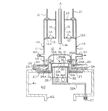
Figure 1 is a schematic front cross-sectional
view of an apparatus of the present invention for the
rapid coating of a substrate 31 with a material,
particularly diamond, wherein the substrate 31 being
coated is supported by a graphite susceptor 31A. The
susceptor 31A is mounted on a substrate support 32 which
stands on a moving stage 32A used to change the position
of the substrate 31. A plasma 30 is created in the
region between the jet pattern controller 35 and the
substrate 31 below orifice 35B by coupling microwave
-7- 2182247
power into the plasma 30. The metal plate 27 and the
controller support 35A are sealed together to force the
source gas to flow through the orifice 35B of jet
pattern controller 35 and into the plasma 30. This gas
flow configuration optimizes the efficiencies of the
source gas and the input power. A heater 36 or cooling
system 36A is added underneath the susceptor 31A to
adjust the process temperature of the substrate 3l to be
coated. Figure lA is an enlarged partial sectional view
of the plasma 30 region and the gas flow orifice 35B,
wherein the gas flow is shown by the arrows. Figure 1B
is a plan view of the pattern controller 35, and orifice
35B.
Figure 2 is a schematic front cross-sectional
view of an apparatus similar to that of Figure 1 showing
one example of a jet pattern controller 35 with multiple
orifices 35C and 35D. Uniform coating over larger
surface areas are achieved with an overlapping multi-jet
plasma pattern through controller 35. Figure 2A shows
an enlarged partial sectional view of the pattern
controller 35 and plasma 30 and the gas flow orifices
35C and 35D. Figure 2B is a plan view of the pattern
controller 35 of Figure 2.
Figure 3 is a schematic front cross-sectional
view of an apparatus as shown in Figure 1 showing drills
60 which are partially covered by the plasma 30 and
showing a gas outlet 70. Figure 3A is a plan cross
sectional view along line 3A-3A of Figure 3.
Figure 4 is a schematic front cross-sectional
view of the drills 60 in a holder 63 and showing the gas
outlet 70 and gas outlets 72 in the holder 63. Figure
4A is a plan cross-sectional view along line 4A-4A of
Figure 4.
Figure 5 is a schematic front view of an
apparatus similar to that of Figure 4 with multiple
openings 61 and support 63 for drills 60. Figure 5A is
a plan view along line 5A-5A of Figure 5.
_8_ 2182247
Figure 6 is a schematic front view of an
apparatus such as shown in Figure 4, wherein a ring seal
64 on a holder 65 is provided in the plasma 30. Figure
6A is a plan view along line 6A-6A of Figure 6.
GENERAL DESCRIPTION
The present invention relates to a method for
treating a substrate with a plasma which comprises:
providing a plasma generating apparatus including a
plasma source employing a radiofrequency, including UHF
or microwave, wave coupler means which is metallic and
optionally including a static magnetic field around the
plasma which aids in coupling radiofrequency energy at
electron cyclotron resonance and aids in confining ions
in the plasma in an electrically insulated chamber means
in the coupler means, mounted in closely spaced and
sealed relationship to an area of the coupler means with
an opening from the chamber means at one end; waveguide
means for coupling the radiofrequency waves to the
coupler means; and a stage means which forms part of the
coupler means and provides for mounting a substrate
adjacent the plasma, a conductive plate with at least
one orifice mounted at the opening from the chamber
between the stage means and the chamber; an inlet and an
outlet for~gas flow through the orifice and through the
plasma to a region between the orifice and the stage
means and onto the substrate, and then removal from the
region; and tuning means for positioning the
radiofrequency waves between the orifice and the stage
means; and generating the plasma in a flow of the gas
between the orifice and the stage means by tuning the
radiofrequency waves which acts upon the substrate.
Further, the present invention relates to a
plasma generating apparatus for treating a substrate
with a plasma including a plasma source employing a
radiofrequency, including UHF or microwave, wave coupler
means which is metallic and optionally including a
static magnetic field around the plasma which aids in
_9_ 2182247
coupling radiofrequency energy at electron cyclotron
resonance and aids in confining ions in,the plasma in an
electrically insulated chamber means in the coupler
means, mounted in closely spaced and sealed relationship
to an area of the coupler means with an opening from the
chamber means at one end; waveguide means for coupling
the radiofrequency waves to the coupler means; and a
stage means which forms part of the coupler means and
provides for mounting a substrate adjacent the plasma,
the improvement which comprises: a conductive plate with
at least one orifice mounted at the opening from the
chamber between the stage means and the chamber; an
inlet and an outlet for gas flow through the orifice and
through the plasma to a region between the orifice and
the stage means and then for removal from the region;
and tuning means for positioning the radiofrequency
waves between the orifice and the stage means.
The apparatus and method is particularly used
for etching and for deposition of materials particularly
diamond thin films. Any treatment of a surface is
contemplated.
Figures 1, lA and 1B show the preferred
improved plasma apparatus of the present invention,
which has elements in common with U.S. Patent No.
5,311,103 issued to the present inventors. The system
is preferably constructed to be operated at 2.45
gigaHertz. A cylindrical metallic or conductive cavity
10 is formed by side wall 11 which is 178 millimeter in
inside diameter, and is open ended. Water cooling tubes
11A are provided. A sliding short 12, which is
electrically connected to the side walls via the finger
stocks 12A, forms top end of the cavity 10. The lower
section of the cavity 10 consists of a bottom surface
13, a base-plate 20, a jet pattern controller 35, a
controller support 35A, a substrate support 32, and the
metal plate 27. The sliding short 12 is moved back and
forth along the longitudinal axis A-A of the side wall
~ 18247
-10-
11 by the moving rods 21 with a conventional gear
assembly (not shown). The excitation probe 14, which is
housed inside the probe sleeve 15, is adjustable with
respect to the sliding short 12 through a set of
mechanical gears (not shown). The adjustable sliding
short 12 and excitation probe 14 provide the impedance
tuning mechanism to minimize the reflected power. The
source gas, which is supplied through the source gas
inlet 25 and annular source gas ring 26, is confined at
the lower section of the cavity 10 by a quartz bell jar
18. The base-plate 20 and quartz bell jar 18 are cooled
by the water cooling channel 23 and gas cooling tunnel
24 through the annular water cooling rings 23A and gas
cooling rings 24A. Also the quartz bell jar 18 is
cooled by cooling gas through the cooling gas inlet 50.
The cooling gas flows over the quartz bell jar 18 and
exits via cooling gas outlet 51.
The substrate 31 to be coated is positioned on
top of a susceptor 31A (preferably graphite) which is
supported by substrate support 32. The substrate
support 32 stands on a moving stage 32A which is used to
change the location of the substrate 31. The metal
plate 27 and the controller support 35 are sealed
together to force the gas to flow through the jet
pattern controller 35, which is a plate with an orifice
35B. A plasma 30 is created in the region between the
jet pattern controller 35 and the substrate 31 below
opening 35B by coupling microwave power into this
region. This construction minimizes the plasma 30
volume by creating a high power density plasma 30
adjacent to the substrate 31. The size and power
density of the plasma 30 are controlled by variation in
input power, pressure, gas flow and substrate 31
position. The jet pattern controller 35 directs the way
that the gas flows through the plasma 30 and onto the
substrate 31. This configuration optimizes the
efficiency of the source gas since there is no gas flow
-11- 21$ 2 2 4'~
by-passing of the discharge as in the prior art devices.
A heater 36 or cooling channel 36A which can be either
a heater or liquid or gas cooling channel placed
underneath the substrate, can be used to control the
process temperature of the substrate 31. The apparatus
is mounted on a vacuum chamber 40 with chamber walls 41
and a chamber conduit 42 leading to a vacuum pump (not
shown). Figure lA shows the close-up view of the plasma
30 region and the gas flow orifice 35B. Figure 1B shows
the orifice 35B. Figures 2 and 2A show one example of
a jet pattern controller 35 with a multi-jet
configuration formed below orifices 35C and 35D.
Uniform coating over larger surface areas can be
achieved with overlapping orifices in multi-jet pattern
controller 35. Figure 2A is an enlarged view of the
controller 35 with arrows showing the gas flow. Figure
2B shows the plan view of the controller 35 and orifices
35C and 35D.
Figures 3, 3A, 4, 4A, 5, 5A, 6 and 6A show the
configurations where the reactor apparatus and method
are used to uniformly coat objects with complex
geometries, such as round (cylindrical) cutting tools.
With an optimized multi-jet pattern controller 35, the
plasma 30 is created to surround the objects
(cylindrical round cutting tool or drill 60) such that
uniform coatings are obtained. The tool holder 62 and
holder support 63 are used to position the drill 60 and
to mask portions which are not to be coated. Figure 6
shows other objects such as seal rings 64 which are
coated with the reactor apparatus and method. These
rings 64 are placed on the ring holders 65. Gas flows
through orifices 61 and out through gas outlet 70.
Holder 63 can include intermediate gas outlets 72.
The experimental microwave circuit used to
deliver power into the reactor is described in U.S.
Patent No. 5,311,103 issued to the present inventors.
It primarily includes (1) a 2.45 gigaHertz, variable
l,
2182247
-12-
power source, (2) circulators and matched dummy loads,
(3) directional couplers and power meters that measure
the incident power P;, and reflected power P,, from which
the power absorbed by the reactor is given by P~ = P;-P"
and (4) the coaxial excitation probe 14 and the cavity
10.
EXAMPLE 1
A reactor apparatus having a cavity 10 with a
178 millimeter inside diameter wall 11, a quartz jar 18
with a 127 millimeter inside diameter, and an end power
feed probe 14 with a 41 millimeters inside diameter
sleeve 15 was built and used .for diamond film growth.
A high power density discharge was created with 550 scan
hydrogen and 14 sccm methane gas flow at 120 Torr with
4000 Watts 2.45 GHz power absorbed. Diamond films have
been deposited on silicon wafers with a linear growth
rate of greater than 100 ~,m/hour on an exposed portion
of the substrate.
Adherent and uniform diamond films were
deposited on cylindrical round cutting tools (drills 60)
and ring seals (seal 64) under a range of experimental
conditions simultaneously: gas flow rates: HZ = 400 & 600
sccm, CH4 = 1, 2, 3 & 4 sccm, CH4/Hz = 0. 25%, 0. 5% & 1%;
pressures: 20, 25, 30 & 40 Torr; jet nozzle sizes:
1/16", 1/8" & 1/4"; quartz tube lengths: 6 cm, 7 cm & 9
cm; tool sizes: lengths: 2" & 2.5", diameter: 5/8" &
1/4"; number of tools coated: 1, 2 & 4; substrate
temperature: 745°C - 970°C; microwave power: 0.36 - 1.25
kilowatts.
EXAMPLE 2
Uniform diamond films were deposited on four
(4) round tools together under the following
experimental conditions: Hz - 400 sccm, CH4 - 2 sccm,
pressure = 25 Torr, 2.45 GHz power absorbed = 660 Watts,
nozzle size = 0.25", number of tools = 4, tools diameter
- 0.25", tool length - 2.5", substrate temperature -
800°C as in Figure 5.
218224
-13-
The present invention preferably uses a
microwave plasma disk reactor (MPDR), described in the
prior art. They include: (1) cylindrical cavity, (2)
internal matching, i.e., sliding short and variable
probe; (3) excitation of TMo," modes for deposition of
f i lms .
The present invention offers advantages over
the apparatus described in the prior art. It ensures
that only the plasma adjacent to the substrate is
produced. Thus the discharge volume is optimized. It
is not any bigger than necessary, resulting in optimized
efficiency of the input microwave power. The source gas
is forced to flow through the plasma and hence the
efficiencies of the input power and source gas are
optimized. This is a different method of creating a
plasma jet discharge from those described in the prior
art. In the jet reactors described in the prior art,
the reactive gases flow through a discharge which is
located upstream from a nozzle. The hot gases are then
forced through the nozzle and projected onto a
substrate. In the present reactor apparatus, the
reactive gases are forced to flow through an orifice or
nozzle 35B (35C and 35D) first. After which they are
dissociated through a plasma 30 which is located
adjacent to but down-stream from the orifice 35B. The
dissociated reactive species are then projected onto the
substrate 31. In the jet reactors described in the
prior art, there is significant amount of volume and
surface recombinations of dissociated reactive species
when they are forced through an orifice or nozzle. The
gas flow and power efficiencies of the reactors are
significantly reduced. Also, when hot gases are forced
through a nozzle as in the prior art, the problems of
erosion and/or deposition and/or melting exist. On the
other hand, in reactor apparatus of the present
invention where the plasma 30 is located downstream from
the orifice 35B, the problem of recombination in the
v..
2182247
-14-
nozzle does not exist. The input gas flow serves as a
natural cooling agent to the orifice 35B and the
problems of erosion, deposition and melting are
drastically reduced or eliminated.
Since the plasma created by this apparatus and
method is relatively independent of the geometry and
properties of the substrates 31 to be coated, it
therefore becomes possible to use this method to coat
objects with complex geometries, such (cylindrical)
drills 60 and seal rings 64. More importantly,
uniformly coatings have been achieved.
Diamond films are uniformly deposited on a
batch (1 - 1000) of round (cylindrical) cutting tools
and seal rings using the configurations displayed in
Figures 3, 4, 5 and 6. The operating conditions are in
the range of pressure 0.1 - 100 Torr, gas flow l0 -
100,000 sccm, microwave or UHF power 0.1 - 100
kilowatts. The number of tools or rings coated is in
the range of 1 1000 at a time. For example, by
dropping the excitation frequency to 915 MHz, a 13"
diameter plasma has been created in a reactor apparatus
with an 18" cavity. If the nearest tools are placed 1"
apart, more than 130 tools can be simultaneously coated
in this reactor apparatus. By placing the tools closer
or dropping the excitation frequency further, more tools
can be simultaneously coated by this reactor apparatus
and method.
It is intended that the foregoing description
be only illustrative of the present invention and that
the present invention be limited only by the hereinafter
appended claims.