Note : Les descriptions sont présentées dans la langue officielle dans laquelle elles ont été soumises.
~1~~051
1
Description
HYBRID CIRCUIT USING MILLER EFFECT FOR PROTECTION OF
ELECTRICAL CONTACTS FROM ARCING
Technical Field
This invention relates generally to arc
suppression and/or extinction circuits for electrical
contacts (contacts through which an electrical current
~ flows) and more specifically concerns such a circuit which
includes an insulated gate bipolar junction transistor
( IGBT) .
Background of the Inyention
With electrical contacts, whether in a high
current circuit, or in the form of conventional relay
output contacts or in other similar circuits, a common
problem is the possible creation of an electrical arc
between the contacts as they begin to open from a closed
position. If the voltage across the opening contacts is
allowed to ris a to a sufficient level, an arc forms
between the contacts. The voltage may even be sufficient
that the arc will continue even after the contacts open
and in an extreme case, the arc may continue even to
maximum contact separation. Arcing is undesirable because
of the wear it produces on the contacts as well as other
circuit effects which may occur due to the arc current
after the circuit should be open.
Typically, the manufacturers of devices such as
relay contacts rate those contacts to switch a certain
voltage and current reliably many thousands if not
millions of times. To guarantee such a performance
rating, the manufacturer typically relies on the inherent
arc suppression and/or arc extinction characteristics of
that particular contact arrangement. Characteristics
which influence a contact's ability to suppress or
extinguish an arc include the smoothness, size and shape
of the contacts, the separation rate, the final maximum
separation distance, and the characteristics of the medium
_ - 218051
2
separating the contacts in their open state.
These inherent arc suppression and/or extinction
characteristics can be augmented.. by placing external
components/circuitry across the contacts which hold the
peak voltage or rate of increase of the voltage across the
contacts to a value compatible with the separation rate
or final maximum separation distance of the contacts. An
example of such an external component is a capacitor.
This technique is shown in U.S. Patent No. 4,438,472 to
Woolworth. Woolworth increases the effect of the shunting
capacitor with a bipolar junction transistor.
Such a technique is not appropriate in many
applications, however, including protective relays in a
power substation. The capacitance may appear as a short
circuit, even when the contacts are open. Further, for
loads which are significantly less than the circuit is
designed for, the time-required for interrupting the load
current is significantly extended.
Another approach involves the control of the
peak voltage across the contacts without regard to their
separation rate. The voltage is limited to a value in
accordance with the rating of the contacts and the
expected load current. This technique allows an arc to
form but limits the peak voltage across the contacts such
that the arc is extinguished by the natural
characteristics of the particular contact arrangement.
This technique, however, limits the operation of the
contacts to rated performance which in many cases is
impractical or otherwise unacceptable.
Disclosure of the Invention
Accordingly, the invention is a circuit capable
of suppression or extinction of arcing across switching
contacts, wherein the circuit includes: an insulated gate
bipolar junction transistor (IGBT), which comprises a
Darlington combination of a field-effect transistor and
a bipolar junction transistor connected across the
218501
3
contacts; and a capacitor, which is connected between a
collector portion and a gate portion of the IGBT, adding
to the stray capacitance of the IGBT, so that the combined
capacitance is such that in response to a current
therethrough, the resulting voltage across the combined
capacitance produces a large enough charge at the gate
portion of the IGBT to turn the IGBT on, which in turn
limits the voltage across the capacitance to a value dust
sufficient to maintain the IGBT in conduction, and wherein
the voltage across the IGBT is sufficiently limited to
prevent arcing across the contacts.
Brief Description of the Drawings
Figure 1 is a circuit diagram showing the arc
suppression and extinction circuit of the present
invention relative to particular contacts being protected.
Figure 2 is a diagram showing a portion of the
circuit of Figure 1 in more detail.
Best Mode For Carrying Out the Invention
The arc suppression and extinction system of the
present invention (hereinafter referred to simply as an
arc suppression system) is designed to operate in
conjunction with electrical and/or electromechanical
contacts which carry a medium range of current, i.e. up
to approximately 10 amps or so.
In one particular application for the present
invention, the electrical contacts to be protected axe
present on the rear panel of, and form output contacts
for, a microprocessor-based relay which is used for
protecting electric power transmission/distribution
systems. In this particular application, the closing of
the electrical output contacts on the rear panel of the
relay by the operation of the relay results in the closing
of a circuit which includes a trip coil for a circuit
,~ breaker connected to an electric power line. The circuit
breaker normally carries very high currents, on the order
CA 02185051 2001-02-19
4
of 1000 amps. When the output contacts of the relay close,
battery power as a result flows to the trip coil circuit,
which in operation, opens the circuit breaker.
It should be understood, however, that the arc
suppression circuit of the present invention can be used to
protect electrical contacts in other applications involving
medium current levels.
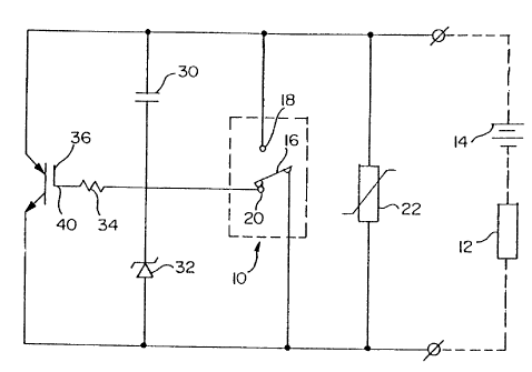
Referring now specifically to Figure l, the
electrical contact circuit application referred to above
(i.e. the microprocessor-based protective relay output
contact circuit) is shown generally at 10. In one
implementation, electrical contact circuit 10 is an
electromechanical circuit known and available commercially
as an OmronTM G6R-1, which has operating characteristics
which are suitable for a microprocessor-based protective
relay. Circuit 10 opens and closes a power system circuit
which includes a circuit breaker trip coil, shown in
Figure 1 as load 12, and a power substation battery 14
which provides power to the load. In the embodiment
shown, battery 14 is nominally 125 volts DC; however, the
battery voltage may in fact go as high as 140 volts DC, due
to battery charging current.
In the embodiment shown, the OmronTM G6R-1 circuit
10 includes a wiper arm 16 which moves between electrical
output contacts 18 and 20. The movement of wiper arm 16 is
controlled by current through a coil 21 which is shown in
the OmronTM circuit in Figure 2.
Wiper arm 16 is shown in Figure 1 in what is
referred to as an "open" position for the circuit 10,
positioned against contact 20. In this embodiment, wiper
arm 16 is normally in that open position. In this
position of the wiper arm, no current will flow in the
circuit because battery 14 is held off by the combination
~
CA 02185051 2001-02-19
4a
of the open position of the contact circuit 10, a metal
oxide varistor (MOV) 22, and an insulated gate bipolar
junction transistor (IGBT) 36. For the circuit shown, MOV
22 is rated at 130 volts RMS, which means that it
~18~0~1
definitely will not conduct up to 180 volts DC, i.e. MOV
22 will block current flow until the voltage across it
exceeds approximately 180 volts DC. In operation, the
voltage is clamped at 250-300 volts by MOV 22 for medium
5 current levels.
The IGBT 36 is a key element in the present
invention, as described in more detail below. An IGBT is
an insulated gate bipolar junction transistor (IGBT),
which is a Darlington-type combination of a field effect
transistor (FET) and a bipolar junction transistor (BJT)
capable of handling high levels of power.
In operation, the FET portion of the device
supplies base drive to the B,TT portion such that the
device as a whole is controlled by the gate of the FET.
The gate drive requirements for an IGBT are thus similar
to those of an FET, while the power switching capability
of an IGBT is much higher than for a similar size FET,
since the voltage drop across the IGBT device is clamped
at about one volt when properly driven. An IGBT device
typically has higher leakage current than the FET portion
thereof does, although the IGBT leakage current is in fact
much less than what is permissible in the arc suppression
circuit shown. In the present case, a suitable IGBT is
an IRGPC40S manufactured by International Rectifier, which
is capable of handling 60 amps and 600 volts.
In the particular protective relay configuration
described above, wiper 16 is in an "open" position when
the circuit breaker in the power system is closed and the
current in the power transmission line is at a normal
level.
When the microprocessor-based protective relay
detects an event such as the current on the power
transmission line being above a preselected threshold, a
signal is applied to the base of transistor 26 in the
Omron output contact circuit, through resistor 27 and
,' zener diode 28. This results in a current through coil
21, which causes wiper arm 16 to begin to move from
- 21$ i0~1
6
contact 20 to contact 18, in effect moving from an "open"
position to a "closed" position. This results in battery
14 producing a current through electrical~output contact
circuit 10, including wiper arm 16, and then back to the
trip coil load 12, thus energizing the coil and resulting
in an opening of the circuit breaker for the power
transmission line carrying the out-of-tolerance current.
' Referring now more specifically to Figure 1,
capacitor 30, diode 32, and the natural gate-to-emitter
capacitance of IGBT 36 form a voltage ramp-type arc
suppression circuit which is suitable for light loads
and/or small contact separation. This capability is used
when wiper 16, having moved away from contact 20, makes
contact with contact 18, at which point load current
begins to flow from battery 14 through contact 18, wiper
16, load 12 and back to the battery. Capacitor 30, which
had previously been fully charged, discharges through
contact 18, wiper 16, and diode 32.
Diode 32 serves two functions in the circuit
shown. It protects the gate-emitter portion of IGBT 36
from destructive reverse bias, and it also allows
capacitor 30 to discharge very quickly. If wiper 16
bounces after initially contacting contact 18, load
current will continue to flow from battery 14, but through
capacitor 30, resistor 34, and the natural capacitance of
the gate-to-emitter portion of semiconductor device 36.
Resistor 34 is chosen to be small enough that the voltage
drop across it for light loads is about 1 volt. As load
current flows through capacitor 30 and the gate-to-emitter
capacitance of IGBT 36, the voltage across the contacts
18-20 is limited and therefore no arc develops.
Referring again to Figure 1, capacitor 30, diode
32, resistor 34 and IGBT 36 form an arc suppression
circuit suitable for heavy loads and/or large contact
separation, such as occurs in the circuit of Figure 1 when
coil 21 in Figure 2 is de-energized, and wiper arm 16 is
moved back toward contact 20 from contact 18. Thus, the
__ zis~o~i
circuit of Figure 1 is able to protect against arcing
between contacts 18 and 20 both when wiper 16 moves away
from its normal position against contact 20 to contact 18
and also when wiper 16 thereafter moves back to contact
20.
The movement of wiper arm 16 back toward contact
20 might be initiated, for instance, in the particular
- embodiment shown when the circuit breaker far the
transmission line has been opened and the out-of-tolerance
l0 current flowing in the power line has been interrupted,
such that the trip coil (load 12 in Figure 1) for the
breaker need no longer be energized. This action is
initiated by a signal generated within the protective
relay which in effect de-asserts transistor 26 (Figure 2) ,
such that transistor 26 turns off, thereby blocking
current into coil 21 of the Omron G6R-1 circuit. When the
coil current is interrupted, flyback diode 25 begins to
conduct, preventing destruction of transistor 26 by high
voltage.
The zener diode 38 in parallel with coil 21 in
the output contact circuit hastens the decay of
circulating current in the coil 21, which was initiated
when transistor 26 began conducting. This produces a
faster action of wiper arm 16, i.e. wiper 16 separates
from contact 18 and moves back to contact 20 in a shorter
amount of time. This is important, since IGBT 36 conducts
and dissipates power when wiper arm 16 is between contacts
18 and 20.
As wiper arm 16 separates from contact 18,
current from battery 14 flows through capacitor 30,
resistor 34 and the IGBT .gate-emitter junction to the
load. Current continues to flow until there is enough
charge accumulated on the gate portion 40 of the IGBT that
the IGBT begins to conduct. Once this threshold gate
charge is reached, the IGBT remains in an "on" condition,
,' without the need for continuous gate drive. Once the IGBT
turns on, the current path through the IGBT will be
zls~o51
8
through the collector-emitter junction to the load 12.
A specific voltage drop equal to the voltage drop across
capacitor 30 plus the voltage drop across the gate-emitter
portion of IGBT 36 is thus maintained along this current
path so that any arc which may initially develop between
contact 18 and wiper arm 16 is extinguished by the
inherent arc extinction characteristics of the contacts.
. Capacitor 30 is important to the operation of
the arc suppression circuit of the present invention.
There is normally a collector-to-gate stray capacitance
in semiconductor devices, referred to as the Miller
capacitance, through which, in the embodiment shown, a
small displacement current can flow from battery 14 to the
gate portion of IGBT 36: The IGBT Miller capacitance and
the IGBT gate-to-emitter capacitance form a capacitive
voltage divider in the circuit of Figure 1. Capacitor 30
was added across the IGBT collector-to-gate junction,
effectively in parallel with the Miller capacitance, to
reduce the voltage rise necessary at the collector of IGBT
36 to provide .the charge at the IGBT gate 40 sufficient
to turn the IGBT on. A 2 nanoferrad capacitor results in
sufficient charge delivered to gate 40 to turn the IGBT
on with a collector-to-gate voltage rise of about 5 volts.
The IGBT is thus maintained,. through this
feedback arrangement, in just the right state of
conduction to keep the voltage across the Miller
capacitance at the required level to maintain the IGBT in
conduction. The circuit basically goes into balance.
The gate voltage necessary to place the IGBT in
the proper conduction state for the maximum expected load
current can be determined from the IGBT data sheet. That
gate voltage is then added to the voltage across capacitor
30 to determine the rating requirement fob the contacts.
For example, for the above IGBT, if the contacts
are to be used to interrupt 10 amps, the IGBT data sheet
indicates that approximately 6 volts on the gate-to
emitter junction of the IGBT is necessary to place the
f
' 21Sa051
9
device in conduction. Also from the same IGBT data sheet,
one can determine that about lOnC of charge must be
delivered to IGBT gate 40 to bring it to 6V. This lOnC
must pass through capacitor 30, resulting in capacitor 30
charging to about 5V. Adding the voltage across capacitor
30 to the voltage at the IGBT gate 40, it can be seen that
a circuit rated to switch 10 amps at 11V is required. The
- Omron circuit mentioned above is rated tv switch 10 amps
at 24V and thus is satisfactory.
l0 Resistor 34 is connected between capacitor 30
and gate 40 of the IGBT to minimize, if not eliminate,
device oscillations caused by the addition of capacitor
30 across the device Miller capacitance. This has the
effect of slowing to some extent the turn off/turn on
response of the IGBT.
When wiper arm 16 reaches contact 20, there is
no longer any need for the arc suppression circuit, since
the contacts have again reached maximum separation. When
wiper arm 16 comes into contact with contact 20, the
charge on gate 40 of the IGBT is carried away very rapidly
through resistor 34, wiper arm 16, and back to the emitter
of IGBT 36. This turns IGBT 36 off. Thus, IGBT 36 is
only conducting while wiper arm 16 is between contacts 18
and 20, substantially reducing the power dissipated by the
IGBT.
When wiper arm 16 comes in contact with contact
20, capacitor 30 is again charged very rapidly so that
subsequent bounces of wiper arm 16 on contact 20 do not
result in IGBT 36 turning on.
With wiper arm 16 on contact 20, the gate-
emitter junction of IGBT. 36 is effectively shorted,
preventing IGBT 36 turning on because of voltage
transients across the open contacts.
After IGBT 36 turns off, load 12 begins to look
like a current source if it is inductive. Metal oxide
,' varistor 22 allows the voltage across it to go to
approximately 250-300 volts, at which point it begins to
-- 215051
conduct. MOV 22 in operation forces the current in an
inductive load to ramp down to zero. When the load
current returns to zero, with wiper 16 against contact 20,
the circuit is back to its initial condition. Since IGBT
5 36 turns off when the wiper 16 reaches its fully open
position against contact 20, the energy in the circuit ig
substantially dissipated in the MOV 22, with some energy
' being dissipated in the IGBT during the time wiper arm 16
is moving from contact 18 to contact 20. This is a
10 substantial improvement over similar suppression circuit
devices when used with inductive loads.
With wiper arm 16 against contact 20, the
magnifying effects of IGBT 36 with respect to capacitor
30 are not present. Thus the total capacitance presented
to the load while the contact is open is limited to the
value of capacitor 30 plus any stray capacitance
associated with the other devices. This is a substantial
improvement over other similar arc suppression devices.
The above explanation with respect to Figures
1 and 2 was for a circuit configuration where wiper arm
16 is in a "normally open" position, i.e. against contact
20. The circuit of Figures 1 and 2, however, is also
effective when wiper arm 16 is in a "normally closed"
position, i.e. against contact 18. In the normally closed
configuration, when there is no current flowing in relay
coil 21 (Figure 2), wiper arm 16 is positioned against
contact 18. When current begins to flow in relay coil 21,
such as under the conditions discussed above when there
is an out-of-tolerance current level on the power line,
wiper arm 16 moves away from contact 18 and eventually
comes into contact with contact 20.
The time during which wiper arm 16 is moving
from contact 18 to contact 20 is important in this
configuration as well, because it is during this time that
the IGBT 36 is conducting. In this case, however, wiper
arm 16 is moving from contact 18 to contact 20 when relay
coil 21 is energized. The goal is to reduce the time that
X185051
11
wiper arm 16 is moving after transistor 26 turns on. This
is accomplished by capacitor 44 (Figure 2) , which provides
a momentary overvoltage to relay coil 21, causing current
and magnetic flux to build up in coil 21 faster than would
be otherwise possible. As capacitor 44 charges, the
overvoltage decreases, preventing the relay from being
damaged by a continuous high level of overvoltage.
' Resistor 42 eliminates the DC blocking
capability of capacitor 44, thereby allowing the relay
l0 coil to be energized for relatively long periods of time.
Hence, with the circuit of the present
invention, it does not matter whether the contacts being
protected are configured to be in a normally open or a
normally closed position. Further, the device which
controls the operation of transistor 26, such as a
microprocessor; need not know how the circuit is
configured. Transistor 26 is turned on when a particular
predetermined power line condition occurs, and turns off
when that condition is corrected.
Hence, an arc suppression and extinction circuit
has been described which utilizes a particular
semiconductor device (an IGBT) and additional capacitance
in parallel with the device's inherent Miller capacitance
to rapidly shunt current away from the opening contacts,
preventing an arc from forming for light loads and/or
small contact separations, and allowing the inherent
characteristics of the contacts to extinguish the arc for
heavy loads and/or large contact separations. In
addition, the circuit is arranged so as to minimize the
energy dissipated in the semiconductor device itself, to
minimize the capacitance presented by the open contacts,
and to minimize the effect of load variations on the
interrupt time of the contacts.
Although a preferred embodiment of the invention
has been disclosed herein for illustration, it should be
understood that various changes, modifications and
substitutions may be incorporated in such an embodiment
218051
12
without departing from the spirit of the invention which
is defined by the claims which follow: