Note : Les descriptions sont présentées dans la langue officielle dans laquelle elles ont été soumises.
WO 95/26561 PCT/US95/03705
1
ELECTRODE STROCTURE AND METHOD FOR
ANODICALLY-BONDED CAPACITIVE SENSORS
BACKGROUND OF THE INVENTION
The present invention relates to capacitive sensors
and, more particularly,.to a sensor in which a frame
surrounding a sensing element is anodically bonded to a
glass layer having a sensing electrode over a portion of its
surface.
Anodic bonding is used to affix and seal glass wafers
to adjacent semiconductor layers in a variety of capacitive
sensing devices, such as pressure sensors, flow sensors and
accelerometers. Anodic bonding occurs between a piece of
sodium-containing glass and an adjacent semiconductor when
the glass is biased to a large negative potential relative
to the semiconductor at temperatures of a few hundred
degrees C. This draws sodium ions within the glass away
from the glass/semiconductor interface, leaving a thin
depletion region. The electric field across the depletion
region is so intense that it breaks bridging bonds in the
glass and draws the resulting oxygen ions toward the
semiconductor. The semiconductor is therefore oxidized near
the interface and chemically bonds the semiconductor to the
glass.
In capacitive sensors of this type, a portion of the
glass layer which is not anodically bonded is coated with a
thin film sensing electrode. In order to avoid arcing, this
electrode is often maintained at the same potential as the
semiconductor body during the bonding process. Thus, a
depletion region is formed in the glass adjacent the. sensing
electrode, as well as adjacent the semiconductor itself,
drawing oxygen toward the electrode. Applicant has
discovered that this results in at least a portion of the
electrode material being oxidized and adversely affects the
accuracy and reliability of the finished sensor. In extreme
WO 95/26561 ~ PCT/US95/03705
2
cases, the electrode material is completely consumed by
oxidation.
In addition, applicant has found that oxidation .
continues while the sensor operates because the electrodes
are typically maintained at a higher potential than the .
glass. This gradually draws additional oxygen toward the
interface and oxidizes the electrode even further. In an
inertial sensor, such as a silicon-on-glass accelerometer,
this causes the gap on either side of a movable sensing
element to change over time and affects the electrostatic
forces required to servo the sensing element back to its
null position. Significant errors can be introduced into
the output of the device in this way.
Examples of capacitive silicon-on-glass accelerometers
susceptible to the foregoing effects are disclosed in:
O'Brien et al. U.S. Patent No. 5,205,171; and Warren, K.,
Journal of the Institute of Navigation, vol. 38, no. 1,
pages 91-99, Spring 1991.
Therefore, it is desirable in many applications to
provide a structure and a method for eliminating the
deleterious effects of anodic bonding in capacitive sensors.
SUMMARY OF THE INVENTION
The present invention incorporates an interfacial
barrier layer, such as a nitride film, between a glass wafer
and a sensing electrode of an anodically-bonded capacitive
sensor to eliminate the migration of oxygen from the glass
to the electrode material. When the capacitive sensor is a
silicon-on-glass accelerometer, the nitride compound is
preferably silicon nitride (Si,N,) formed by a suitable thin
film deposition technique. Such techniques include plasma-
enhanced chemical vapor deposition (PECVD) followed by a
suitable patterning step and, in a specific embodiment,
reactive sputtering of silicon in a nitrogen-containing
atmosphere.
WO 95/26561 ~ ~ 8 5 ~ 3 2 PCT/US95/03705
3
Accordingly, the sensor of the present invention may
include: a sensing element having a frame structure; at
. least one glass layer anodically bonded to the frame
structure and having a metallic sensing electrode adjacent
the sensing element; and an interfacial barrier layer
disposed between the glass layer and the metallic sensing
electrode. In one embodiment, the device is an inertial
sensor, such as an accelerometer, having: a substantially
planar proof mass hingedly connected to a frame structure,
the proof mass and the frame structure comprising a
monolithic silicon body; a pair of glass layers anodically
bonded to oppositely-directed surfaces of the frame
structure and having a metallic sensing electrode spatially
opposed to the proof mass; and an interfacial nitride film
between the glass layer and the metallic sensing electrode.
A glass layer may be provided on either side of the proof
mass and frame, and the interfacial film may comprise
silicon nitride.
The structure and method of the present invention are
intended to protect the integrity of a sensing electrode
during an anodic bonding process without adversely affecting
adhesion between the sensing electrode and an associated
glass layer. In addition, they are intended to reduce
changes in the operating characteristics of an anodically-
bonded capacitive sensor during its useful life and to
eliminate failures of anodic bonds in capacitive sensors.
BRIEF DESCRIPTION OF THE DRAWINGS
The above and other features of the present
invention may be more fully understood from the following
detailed description, taken together with the accompanying
drawings, wherein similar reference characters refer to
similar elements throughout and in which:
WO 95/26561 21 B 5 ~ 3 2 PCT/US95/03705
4
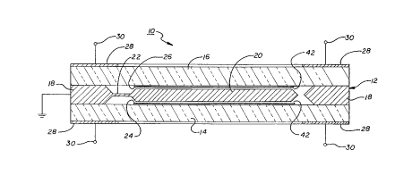
FIGURE 1 is an exploded perspective view of a
capacitive sensor constructed according to a preferred
embodiment of the present invention;
FIGURE 2 is a somewhat schematic horizontal
sectional view of the capacitive sensor of FIGURE 1 taken
along the line 2-2;
FIGURE 3 is a schematic representation of the
capacitive sensor of FIGURE 2 showing the depletion region
formed during anodic bonding and the movement of ions within
the glass under the influence of a bonding potential;
FIGURE 4A is an enlarged fragmentary sectional
view corresponding to a portion of the capacitive sensor of
FIGURE 2, illustrating an electrode configuration of the
prior art; and
FIGURE 4B is an enlarged fragmentary view of a
portion of the capacitive sensor of FIGURE 2 showing an
interfacial barrier layer constructed according to a
preferred embodiment of the invention.
DESCRIPTION OF THE PREFERRED EMBODIMENTS
Referring now to FIGURE l, which illustrates a
preferred embodiment of the present invention, a capacitive
sensor l0 is made up of a semiconductor body 12 sandwiched
between a glass base layer 14 and a glass top layer 16. The
semiconductor body 12 has a peripheral frame portion 18
anodically bonded to each of the base layer 14 and the top
layer 16, and a central sensing element 20 connected to the
frame portion 18 through flexures or "hinges" 22. The base
layer 14 and the top layer 16 are provided with sensing
electrodes 24 and 26, respectively, on surfaces facing the
sensing element 20, to detect movement of the sensing
element under the influence of external forces. When the
CA 02185532 1998-12-31
capacitive sensor 20 is an accelerometer or other inertial
sensor, the sensing electrodes 24 and 26 are also used to
apply electrostatic forces sufficient to return the sensing
element to its neutral position. The sensing element 20
5 thus serves as a force-balanced proof mass supported for
hinged movement within a free space between the electrodes
24 and 26. Electrical connection is made to the sensing
electrodes 24 and 26 through contact pads 24' and 26',
respectively. Accelerometers of this type are described in
0'Brien et al. U.S. Patent No. 5,205,171 and Warren, K.,
Journal of the Institute of Navigation, vol. 38, no. 1,
pages 91-99, Spring 1991.
In accordance with the present invention, an
interfacial barrier layer 46, shown specifically in FIGURE
48, is disposed between the sensing electrodes 24 and 26 and
the respective glass layers 14 and 16. This interfacial
layer acts as a barrier to migration of oxygen from the
glass layers and thereby prevents oxidation of the electrode
material during fabrication and operation of the sensor.
Although for convenience the present invention is
described with respect to an inertial sensor, and
specifically a silicon-on-glass accelerometer, the teachings
apply equally well to other forms of capacitive sensors in
which glass layers are anodically bonded to a structure
containing a sensing element. Such sensors include pressure
sensors and flow sensors in which a diaphragm is acted on by
a fluid being measured. They have a structure corresponding
to the semiconductor body 12, except that the sensing
element 20 is replaced by a diaphragm. This diaphragm is
deflected under the influence of fluid pressure or flow
conditions, and the deflection is measured by sensing
electrodes.
With reference to FIGURE 2, the capacitive sensor 10
has bonding electrodes 28 at the periphery of outwardly-
directed surfaces of the glass base layer 14 and the glass
top layer 16 for applying the electrical potential required
WO 95/26561 PCT/US95/03?OS
6
for anodic bonding. This potential is applied through
bonding terminals 30 (see also FIGURE 2), with the
semiconductor body 12 being grounded.
Referring now to FIGURE 3, in the bonding process a
potential of -400 volts is applied to the terminals 30 while
the device is maintained at a temperature of approximately
300 degrees C. This draws positively-charged sodium ions 32
within the glass toward the bonding electrodes 28 and away
from the peripheral frame portion 18 of the semiconductor
body 12. Because the sensing electrodes 24 and 26 are
maintained at the same potential as the semiconductor body
12, sodium atoms are drawn uniformly downwardly within the
glass base layer 14 and upwardly within the glass top layer
16, thereby depleting free positive charge carriers from the
innermost surfaces of the two glass layers. Thus, the
bonding potential establishes a thin depletion region 34
adjacent the inwardly-directed surfaces 36 of the glass
layers 14 and 16. In this configuration, most of the
applied potential is felt across the depletion region due to
its high resistivity. The depletion region is thin
(approximately one micron) and the resulting field is quite
intense. As a result, bridging oxygen atoms in the silica
network of the glass are drawn toward the glass/silicon
interface in the form of negatively-charged ions designated
38 in FIGURE 3. These ions oxidize the silicon atoms at the
interface to chemically connect the silicon and the glass.
The sensing electrodes 24 and 26 are maintained at the
same potential as the semiconductor body 12 during the
anodic bonding process in order to avoid arcing and possible
sticking of the sensing element 20 to the electrode metal.
This causes oxygen ions to migrate toward the electrodes, as
well, resulting in anodic oxidation of the electrode
material. In extreme cases, the electrode material is
completely consumed by oxidation, causing a loss of adhesion
to the glass. In every case, at least some of the electrode
is consumed if a barrier layer is not provided in accordance
with the present invention.
WO 95/26561 PCT/US95I03705
218532
An additional result of oxidizing the material of the
sensing electrodes 24 and 26 is illustrated schematically in
FIGURE 4A, wherein the thickness of the sensing electrode 24
is increased in thickness so it encroaches upon the
capacitive gap of the device to the extent indicated at 40
in FIGURE 4A. Due to the extremely small distances between
the various elements, this causes a significant reduction in
the operative gap from an initial value 42 to a subsequent
value 44. Even if failure of the device does not occur from
loss of adhesion, a reduction in the gap between the sensing
element and the electrodes seriously affects the accuracy of
the device.
Oxidation also continues at a slower rate during normal
operation of the sensing device 10 when a barrier layer is
not used. This occurs because the electrodes are typically
more positive in potential than the sensing element. At
operating temperatures of approximately 85 degrees C and
above, the potential is capable of drawing negatively
charged oxygen ions from the glass toward the electrode,
further reducing the capacitive gap of the device.
Referring now to FIGURE 4B, the interfacial barrier
layer 46 is provided according to the present invention
between each of the sensing electrodes and the corresponding
glass layer 14 or 16. In a preferred embodiment, the
electrodes 24 and 26 are formed of a gold conduction layer
deposited over a titanium adhesion layer. Specifically, the
sensing electrode 24 of FIGURE 4B is made up of a gold
conduction layer 124 deposited over a titanium adhesion
layer 224. The sensing electrode 26, which is not shown
separately in detail, is then the mirror image of the
sensing electrode 24. The barrier layer 46 is preferably a
nitride compound, and most preferably silicon nitride. The
barrier layer 46 is preferably at least a few hundred
angstroms thick, and most preferably between 800 and 1000
angstroms thick, and may be formed by any suitable thin film
process including, for example, plasma-enhanced chemical
vapor deposition (PECVD) or reactive sputtering. Of these
WO 95/26561 PCT/US95/03705
2185532
8
processes, reactive sputtering is preferable, particularly
when an ion beam is used, because it is carried out at low
temperatures and is relatively directional.
With respect to materials of construction, the base
layer 14 and the top layer 16 may be any sodium-containing
glass suitable for anodic bonding. Glasses having
appropriate sodium contents include, by way of example,
glass manufactured by Corning under the trademark "Pyrex",
that manufactured by the Schott Glass Company under the mark
"Tempax", and comparable glass manufactured by the Hoya
Glass Company. The semiconductor body 12 can then be any
suitable crystalline semiconductor, such as single crystal
silicon, formed by anisotropic etching of a silicon wafer.
The etching process, which is well-known in the art, is used
to form the sensing element 20 and the flexures 22 in the
configuration shown in FIGURES 1 and 2. Alternatively, the
body 12 can be made of any other suitable semiconductor
material which has appropriate elastic properties and is
capable of being etched or otherwise configured in the
required manner. One example of such a material is
germanium.
The glass layers 14 and 16 are preferably approximately
500 microns thick and the semiconductor 12 is preferably
approximately 300 microns thick at the peripheral frame
portion 18. The sensing element 20 is then reduced in
thickness by etching to provide gaps 42 approximately 3
microns across with the sensing electrodes in place. Each
of the sensing electrodes 24 and 26 is preferably
approximately 2500 angstroms thick, which in the embodiment
of FIGURE 4B is a composite film made up of a titanium
adhesion layer (such as the layer 224) approximately 200
angstroms thick adjacent the barrier layer 46 and a gold
conduction layer (such as the layer 124) approximately 2300
angstroms thick. These metals are preferably deposited
sequentially without breaking vacuum according to a suitable
thin film technique, such as sputtering. As described
above, the interfacial barrier layers 46 (see FIGURE 4B)
WO 95/26561 PCT/US95103705
21 X35532
9
between the glass layers and the corresponding sensing
electrodes add from a few hundred angstroms to approximately
1000 angstroms to the overall thickness of the electrode
structure. These thicknesses are accommodated in the
structure of the FIGURES 1 and 2, however, to yield a
capacitive gap of approximately 3 microns on either side of
the sensing element 20.
Although the barrier layer 14 is preferably silicon
nitride, other materials can be used in place of silicon
nitride as long as they bond well to the glass layers 14 and
16 and provide adequate adhesion to the metals of the
electrodes 24 and 26. One such material is titanium
nitride.
In fabricating the capacitive sensor 10, and
particularly the interfacial barrier layer 46, it is
important to minimize any adverse effects on the glass base
layer 14 and the glass top layer 16 from exposure to heat or
chemicals during the deposition and patterning steps. One
process for depositing the barrier layer 46 is plasma-
enhanced chemical vapor deposition (PECVD), in which a
silicon nitride layer is deposited from a plasma containing
dichlorosilane and ammonia at a temperature of approximately
385° C. Glass wafers coated in this way show some tendency
to warp during processing, but are generally acceptable.
They are then patterned by an etching process to remove
silicon nitride from all areas other than those on which the
sensing electrodes 24 and 26 are to be formed. In actual
practice, the layer of silicon nitride is typically provided
over an area slightly larger than the subsequent electrode
metallization in order to avoid direct contact between the
electrode metal and the glass. Although the plasma-enhanced
chemical vapor deposition process results in usable devices
which do not exhibit the migration/oxidation problems of the
prior art, it can undesirably roughen the glass in the
region of the anodic bond and leach some of the sodium from
the areas etched. Both of these effects render subsequent
anodic bonding more difficult.
WO 95/26561 ~ ~ ~ ~ ~' J ~ PCTlUS95/03705
A preferred method of depositing the barrier layer 46,
and particularly a barrier layer of silicon nitride, is
reactive sputtering. In the process, an ion gun is used to
sputter a silicon target in a nitrogen-containing
5 atmosphere. The gun preferably emits either nitrogen or
argon ions and the substrate may be heated to approximately
70 degrees C'. The process is therefore a low temperature
process which does not adversely affect the glass wafers and
is relatively directional. The barrier layer 46 can
10 therefore be patterned either by a conventional "lift-off"
photoresist process or by depositing the barrier layer
through a shadow mask, eliminating the need to etch or
otherwise disturb the glass surface in the region of the
anodic bond. Either of these patterning methods leaves an
entirely undamaged surface for use in the subsequent bonding
step. The atoms of silicon nitride deposited by reactive
sputtering are also more densely packed than when deposited
by plasma-enhanced chemical vapor deposition. This results
from both the higher energy of the sputtered atoms and the
absence of hydrogen from the deposition environment.
While the preferred embodiment has been described and
illustrated, various substitutions and modifications may be
made thereto without departing from the scope of the
invention. Accordingly, the present invention has been
described by way of illustration and not limitation.