Note : Les descriptions sont présentées dans la langue officielle dans laquelle elles ont été soumises.
WOg~/301~3 21 ~6467 P~ 3~7
.
PHOTOCONDUCTIVITY RED~CTION IN CADMIUM TELLURIDE
FILMS FOR LIGHT BL~CKING APPLICATIONS USING
NITROGr:~ INCORPORATION
BACKGROU~'D OF THE INVENTION
1. Technical Field
The present invention relat~s to liquid crystal light valves (LCLV's), and
more ~al Li- u~ ly to a liquid crystal light valve employing an improved cadmiumtelluride light blocking layer.
2. Discussion
Liquid crystal light valves have diverse a~li~li~,.,~ as light amplifiers,
projectors and image processors. One prior LCLV is disclosed in U.S. Patent
No. 4,019,807 assigned to Hughes Aircraft Company, and which is herein
UldL~ by reference. The light valve of that patent employs successive
device laye}s ~ Iitillg a cadmium sulfide (CdS) ph~ ..".l~ , a cadmium
telluride (CdTe) light absorbing layer, a dielectric mirror, an insulting silicon
dioxide layer and a liquid crystal layer. This device structure is ~ dwi~ d
bet veen indium-tin-oxide l~dl,~al~llL electrodes deposited on an optical quality
glass flat substrate. The particular function of the CdTe light absorbing layer is
WO 95/30173 PCTIUS95/05417
to provide several orders of magnitude o~ light blocking to prevent high intensity
light from saturating the photoconductive layer.
U.S. Patent No. 4,799,773 assigned to Hughes Aircraft Company discloses
an improved LCLV device featuring an d~.lulluhuu~ silicon conductive layer and
a dielectric mirror layer employing titanium dioxide (TiO2). A special bonding
structure is used to bond a cadmium telluride light blocicing layer to the
a.llullJlluus silicon. A titanium dioxide-silicon dioxide layered dielectric mirror
is then applied to the cadmium telluride light blocking layer.
The titanium dioxide layer disclosed in U.S. Patent No. 4,799,773 provides
greatly improved resoiution and spectral ~ :~r~hiiitif ~ The dlll~ JllOU~ silicon
~u~llibu~. ~ an improved r~ response time, d~lJlOa~ the speed
required for raster scan displays. The special bonding structure ties the structure
together and CUIlllibul~,;, to an overall i~ lu.~lll.lll in repeatability. The
bonding structure includes successive layers comprising first and second SiO2
layers and first and second CdTe blocking layers. The adjacent SiO2 and CdTe
layers are oxgyen enriched and the device, including the bonding structure, is
annealed prior to application of a CdTe layer to redistribute the oxygen. U.S.
Patent No. 3,824,00~ assigned to Hughes Aircraft Company, also discloses the
use of CdTe as a light blocking layer. Both U.S. Patent Nos. 4,799,773 and
3,824,00~ are herein ill~Ul~JUldlC;i by reference.
Most commonly, the cadmium telluride light blocking layer is applied using
anuvd~,ul~ ullprocess~ However,forhighll..u~ ,u~d~ Liu..~,~v~pul~liul.
is not suitable because it is too slow, the equipment is costly, labor and overhead
.... ..... . . _ . _ . . _ .. ... = . . , . _ _ . . . . . . . .. .. . ... .... . . . .. .
WO 95/30173 1 ~,IIU,.,.. '~
21 86467
are high, and the vacuum must be broken during the m~n~rtllrjng process.
Thus, it would be desirable to provide an alternative to the ~valJu~Liun processfor producing a cadmium telluride light blocking layer in LCLVs in high volume
applications.
S Sputtering is an alternative process which avoids many of the dia~ldv.~ .g. .,
of f Vd,UUl~liUII Sputtering improves ~IllUU~ , requires less costly eql.irmf ntrequires lower labor and overhead, and does not require breaking vacuum during
the process. However, the ~. ~ru~ allce of LCLV's using sputtered cadmium
telluride light blocking layers have not been entirely a~l~ia~d~UIy. This is because
lû of a rhf nnmr-nnn called "rhntr~h~r~in~" Phu~oal,adi.,g results in uneven output
brightness across the area of the LCLV. It appears to be related to an
instability in r~ livi~y, since it is not i"~ f Iy apparent but only
manifests after a burn-in period.
The causes of rhntnch~rlinfo are not completely ".,rl~ . o. -n-l However, the
rhf .~.",.. ~.. , does seem to be related to the CdTe sputtering target. That is,
pllu~ualladillg iS much worse with some targets than others. However, with high-volume, cost-sensitive applications, it is impractical to use only certain targets,
particularly since it is not certain in advance which targets will produce
photoshading and which will not.
Accordingly, it would be desirable to provide a technique for sputtering
cadmium telluride light blocking layers in LCLVs which yields stable devices that
do not exhibit rhntr~ch~rlin~. It would further to be desirable to provide such a
technique which is illf~ llaiv~ and easily ;",~ r/1 for high-volume
WO95/30173 2186467 r~.~u,,,~ s~l7
applications. Also, it would be desirable to provide a technique for sputtering
cadmium telluride light blocking layers which cAn tolerate normal variations in
cadmium telluride targets and which does not produce phntnch~lin~ with certain
targets. Further, it would be desirable to provide such a technique which results
in low particulate on the light blocking layer.
SUMMARY OF THE INVENTION
Pursuant to a first aspect of the present invention a liquid crystal light valveis provided which includes a substrate and a rhntn~nn~ tive layer formed on
the substrate. A blocking layer comprised of cadmium telluride doped with
nitrogen is formed over the plluLc,colldu.,liv~ layer. A mirror layer is then
formed over the light blocking layer. In a preferred PnnhoflimPnt, bonding layers
are utilized below and above the light blocking layer to improve the bonding of
the light blocking layer to adjacent layers.
In accordance with the another aspect of the present invention a method
for producing a light blocking layer in a liquid crystal light valve is provided.
The method includes the step of sputtering a cadmium telluride blocking layer
in an ~ U~ ,Ie containing an argon and nitrogen mixture.
As a result, the present invention provides a liquid crystal light valve and
a method for producing such light valves which provides an improved cadmium
telluride light blocking layer which can be generated by means of sputtering at
high volume and which does not produce undesirable rhntncll~lin~ effects.
WO 95/3~173 PCl`JUS95)0S4~7
~ 2~ 86467
BRIEF DESCRIPTION OF THE DRAWINGS
The various advantages of the present invention will become apparent to
one skilled in the art by reading the following ~l.c. ;r;. ~t;..,, and by referenee to
the following drawings in which:
FIC. I is a diagram of a liquid crystal light valve utilizing the eadmium
telluride light bloeking layer in a~co..ld.,cc with a preferred embodiment of the
present invention;
FIG. 2 is a flow block diagram illustrating the fabrieation of a liquid erystal
light valve deviee aeeording to a preferred .,lllbc)dilll."ll of the present invention;
and
FIG. 3 is a graph of the switching ratio of the liquid crystal light valve
deviee in accu.da..~,c vith the present invention at various levels of nitrogen in
the eadmium telluride layer in ac~,u.d~ ce witll a preferred c..lbo-lilll.,.l~ of the
present invention.
DETAILED DESCRIPTION OF THE PREFERRED EMBODIMENTS
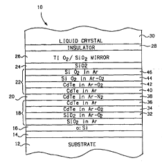
The preferred LCLV structure is shown in cross-section in FIG. 1. The
LCLV 10 includes a suitable glass substrate 12, an indium-tin-oxide (ITO) layer
14, and ~ u~ uu~ silieon rl~ ljv~ layer 16, a first silieon bonding
structure 18, a CdTe bloeking layer 20 a seeond silieon bonding strueture 22, an
SiO2 layer 24 and a TiO2/SiO2 dieleetrie mirror 26. On top of mirror 26 is an
insulator layer 28 and a liquid crS~stal 30. The silicon bonding structure 18
includes four layers 32, 34, 36, 38. The four layers 32-38 respectfully comprise
WO 95/30173 2 1 ~ 6 4 6 7 F~~ '4l7
a first layer 32 of silicon dioxide (SiO2), a second oxy~en-rich layer 34 of silicon
dioxide, an oxygen rich layer 36 of CdTe, and a second layer 38 of CdTe.
The first SiO2 layer 32 is fabricated by deposition in an argon ~ lUD~ C,
while the second oxygen-rich layer of SiO2 34 is deposited in an ~ IU~ C
S co.. ,u~ lg argon and oxygen. The first oxygen-rich layer 36 of CdTe is
deposited in an ~ --u~,ul--,-c also UJIII~Jli~ill~ argon and oxygen, while the second
CdTe layer 38 is deposited in an a~ o~ c of pure argon.
Above the second CdTe layer 38, the CdTe blocking layer 20 is deposited.
The CdTe layer 20 is deposited in an argon-nitrogen atl..u~ c as described
in more detail below. Above the CdTe layer 20 a second silicon bonding
structure æ iS deposited. This silicon bonding structure 22 comprises four layers
40, 42, 44 and 46. The silicon bonding structure 22 is identical to the previous
silicon bonding structure 18 except that the order of the layers are reversed.
Thus, layer 40 is the same as layer 38, layer 32 is the same as 36, layer 44 is the
same as layer 34 and layer 46 is the same as 32. The silicon bonding structures
18 and 22 improve the adherence of the CdTe to minimize the occurrence of
peel up and blister.
Above the SiO~ layer 46 an SiO2 layer 24 is deposited- Above the SiO2
layer 24 is the TiO2/SiO2 dielectric mirror 26, which included 24 layers which
alternate between TiO2 and SiO2. Further details of the rest of the structure and
construction of the LCLV is as known in the prior art and shown for example
in U.S. Patent No. 4,019,807.
~ WO 95/30173 2 18 6 4 6 7 r~.~u~ 7
It should be nûted that the cadmium telluride li~ht blocking layer 20 must
be highly resistive and also must be highly absorptive to maintain opacity. The
narrow band sc.,,;..,,..ll.~ l.., nature of cadmium telluride is suited to this
application. ul~rul ~ullal~ly, when the CdTe light blocking layer is sputtered, the
above-discussed ~ ;v~: properties with resultant ph."~ .l,.,e is
observed. In particular, it appears that when the atomic ratio of the material is
near one-to-one cadmium to tellurium, the result is an unstable and non-uniform
~ ulldu~livily that varies over time. It is thought that the problem ~vith the
controlofcadmiumtelluride~l.l;,l.;.,..,~l,yisduetothesensitivityoftheatomic
ratio to conditions in the immediate area of the sputtering which results in
drastic swings in the deposited film Cllald~ . This results in an
n~rrept~hlr rhntr,ch~rline ~ for liquid crystal light valve
a~,uli~ d~iul,~. As discussed above, while the prior approach of ~vdpulaLill~ the
cadmium telluride light blocking layer does not produce phulu~llaulillg it is not
suited to volume production because of handling (loading and unloading the
system), ~IIluu~ ul (long cycle times are mandated) and associated processing
issues such as annealing and other processes such as il.~ di~ hole
fl;,.,;",.l;r"~
In order to achieve the advantages of sputtering without the resultant
pl~ulO~lladillg problem, the present inventors have discovered that the
ill~UI~UldtiUII of nitrogen into the cadmium te]luride light blocking layer
eliminates the instability and reduces the photoconductivity which apparently
causes the rh.. lll~ rl,f.,.""~ ",l" While some sputtering targets do have
WO 95/30173 2 1 8 6 4 6 7 r~l~o~ ~5iil7 ~
an atomic ratio that appears to preclude this ~ u~ u~ uctivity, the target
", .,,,.8.~ ; processes is not Itlu-ud-lciblc and obtaining consistent targets is
extremely difficult, costly and unpredictable. Furthermore, the sputtering targets
that do produce films with low or no rh"lu~ ",~ ivily are not necessarily those
which have the lowest particulate production so that the quality of the display
cannot be optimized. One alternative approach is the alteration of the
sputtering process which can alter the film properties but this approach does not
alter these properties ~urG~ lly and does not permit the ~;,.",lI"nF.
.";1l;.ll;, ~ of the pal~i~ ula~e density.
1û The addition of nitrogen to the CdTe layer in accordance with this
invention is easily controlled to a very precise level with wide fiexibility using
well-known Ic"llllol~ (e.g., mass fiow controllers) and can be used with targetsand sputtering conditions that do optimize the quality aspects of the deposited
film and hence the resultant LCLV display. FUILII~,IIIIUI~, the cost of nitrogenis almost negligible when compared to the high cost of finding otherwise
acceptable targets. Nitrogen is widely available in high purity.
There are two easily ;~ rd methods for adding nitrogen to the
sputtering process: 1) the use of a cylinder of premixed argon and nitTogen at
the desired percentage, or 2) the use of a manifold mixing system appended to
the sputtering system with mass flow controllers to adjust the mixture in a
precise fashion. The latter method is preferred in a~ul;idll~e with the present
invention. The pressure is m~int~inFri as without nitrogen addition, by a throttle
WO 95/30173 PCT/US9SJD5 117
21 86467
valYe on the vacuum pump. No changes in power, pressure or other
are necessary.
It should be noted that the level of nitrogen is important. At levels that
are too high, a brittle film is obtained and ~ud~ uldlcs are difficult to control.
At levels of nitrogen that are too low, rl~ uc, .~ , livily will be present to an
increasing degree. The ideal pCl~.llld~;C of nitrogen (that is, mole ptl~,~.ll1013C
as opposed to weight ~U~ ,CIIId~l,) has been found to be d,U~UIUAillldl~ one
percent. At 0.25 percent there may be insufficient nitrogen, and at 2.0 percent
there are problems with poor ...~ stability. The ability to vary the
nitrogen also allows the sputtering to operate at powers which permits the
U,Ulillli~.lliUll of cosmetic properties while adjusting the nitrogen level to correct
the electrical properties to achieve an optimum for both pdldlll~lC-~.
Referring now to FIG. 2, a step by step process for depositing the cadmium
telluride light blocking layer and bonding layers in accordance with a preferredCtlllbOll~ ll of the present invention is shown. This process may be carried outon a CUllllll~ idlly aYailable machine such as the PDS II In-Line Sputter System,
m~nllf~rtllred by M.R.C Corporation of Orangebury, N.Y.
According to this process, the glass substrate 12 is first cleaned (step 48)
by sputtering etching at 2û0 watts in 7.75 i 0.25 microns of argon for three
minutes. Allc~l~dliv~lr this step can be omitted. The substrate will already have
the electrode 14 and dlllUl~JIlUU~ silicon photncnnrl~lrtnr layer 16 forrned on top
in accollldll1e with the technique taught in U.S. Patent No. 4, 799,773. Silicondioxide is then sputtered in the DC mode onto the substrate 12 for eight minutes
WO 95/30173 r~ u.,,~ 417
21 ~`67 ~
at 20n watts in 7.75 i 0.25 micr~lns o~ argon (step S0). At the end of step 50,
the oxygen-poor SiO2 layer 32 is formed.
With the silicon plasma stlll running, the ~ s~uh~.~ is changed to an
argon-oxygen mixture comprised of 7.75 i 0.25 microns argon and 2.00 i 0.25
microns of o~ygen giving a total mr~ture pressure of 9-75 i 0.25 microns. The
silicon sputter in this argon/oxy~n mix shown in step 52 is continued for eight
minutes.
At the end of the eight mir.~e argonlo~tygen sputter, step 52, the substrate
is allowed to soak for five minutes in the argon/o?ygen mixture with the RF
generator turned off, step 54. The SiO2 layer 34 is thus formed. Next, in step
56, CdTe is sputtered in the RF Inode onto the SiO2 layer 34 for eight minutes
at 200 watts in the 9.75 i 0.25 r~icrons of argon and oxygen. In step 58, the
structure is allowed to soak in ehe argon/oxygen mixture for another five minutes
with the RF generator off. At the. end of step 58, the oxygen containing CdTe
layer 36 is formed.
After soaking according to step 58, a second eight minute sputter of CdTe
is performed, step 60. The second sputter operation 60 is performed at 200
watts and in an d~l..u"uhc,c of 7.75 i 0.25 microns of argon to in the RF mode
form the second CdTe layer 38.
It should be noted that the above-discussed U.S. Patent No. 4,799,773
teaches the above-discussed steps for providing a bonding layer. However, that
patent discloses the use of annealing process after step 60. Yet, the present
inventors have found this slep ullll- cci,a~uy and have achieved ~ ra~uiy results
WO gS/30173 r~ ..,r~cs~s J
~ 21 86467
11
without annealing. This is hecause in the ahove-described in-line system the
sputter ~ are done without breaking vacuum in rapid succession so the
equivalent of annealing is done before the films are exposed to air. Also, that
patent discloses a sputtering process with bias and in the preferred ~ .,.ho~
of the present invention the sputtering is done without bias. Further, It shouldbe noted that the above-described soak process can be eliminated with
satisfactory results.
Next, the CdTe layer 20 is applied in step 62. In the preferred
. . "l ,o.l., l ,~ . ,l CdTe is sputtered in the RF mode without bias for about one hour
at about 500 watts by adjusting the flow rates ~lu~ul~iulla~ with mass flow
controllers and keeping the pressure constant at about 11 microns. As a result,
the nitrogen content is dl~UlU~illlat~ly one percent. However, the nitrogen
a~s~, may be varied with varying results as discussed in more detail below.
Also it will be a~ . idtcd the power, time period and other l~alal~ a may be
varied to optimize for specific a~,~li. dLiu.. ~. As a result of this process in step
62, two microns of CdTe in argon plus nitrogen are applied. It will be
dlJ~Ic~ ia~cd that this thickness of CdTe will provide an optical density of about
5.
Next, the silicon bonding layer 22 is applied. This involves step 64 (which
is the same step 60), step 66 (which is the same as step 58), step 68 (which is the
same as step 56), step 70 (which is the same as step 54), step 72 (which is the
same as step 52) and step 74 (which is the sarne as step 50).
wo 95/30173 P~ .,S ~
21 ~646~ --
12
Next, in step 76, the SiO2 layer 24 is sputtered to a thickness of l,600
angstroms. The TiO2/SiO2 mirror is thereaher applied by deposition p~UCc~ul~
known in the art in step 78. Finally, the insulator layer 28 and liquid crystal
layer 30 are applied using knûwn techniques.
Referring now to FIG. 3 there is shown a graph of the results of an LCLV
produced with a CdTe light blocking layer doped with nitrogen in accûrdance
with the present invention. This graph plots the switching ratio verses
wave~ength. The switching ratio is a measure of the rh..ln~.~,..l". ~ivi~y, which
results in the phnt-~ch~iing affect. In particular, these Ill~,C~UI~ . are takenby depositing a CdTe layer on a substrate having ITO on top. A silver spot is
then applied to the CdTe layer which is d~ lurillld~ely one-eighth inch in
diameter. Six volts is applied between the silver spot and the ITO layer and thecurrent through the CdTe with no i~ nnin:3tinn on the photodetector is
measured. Next the current is measured with a frxed ill,.",;"t.ll~.., of 200 micro
watts per square C~ l. Finally the ratio between the two Ill. a~ulclll. .
is taken. An ideal ratio of zero would mean that there is no current with no
ill,,,, .;., .1;. ." All the data is taken at a sputtering RF power of S00 watts. "Mag"
indicates data taken with a special magnet, in particular, the magnet behind thetarget commonly used with "111~.~511(,~1UII sputtering" to confine and intensify the
plasma for high sputter rates.
All the data is taken either with the substrate as the innermost rotation
point or the outermost point which is designated in FIG. 3 as "in" or "out". Thefirst curve 80 thus, illustrates results at ~00 watts RF power with the special
... .. . . . _ . _ .... . . ... .. . . .. . . . . .. ... .
Wo95/30173 r~ l/U~ C~117
~ 2~ 86467
13
magnet and at the innermost rotation point of the substrate. Curve 82 is the forsame conditions as curve 80 except that the substrate is at the outermost rotation
position. Both curves 80 and 82 are taken with no nitrogen in the CdTe light
blocking layer 20. Next, curve 84 shows the results for 500 watts power with twopercent nitrogen and 98 percent argon in the sputtered CdTe layer 20, with the
substrate in the outermost position. Curve 86 is the same as curve 84 with the
substrate in the innermost position. Curve 88 shows data taken at 500 watts at
0.5 percent nitrogen and the substrate at the innermost position, while curve 90illustrates data taken with the same conditions as curve 88 except that the
substrate is at the outermost position. Curve 92 illustrates data taken at 500
watts with a nitrogen level of 0.25 percent at the outermost and with the
substrate position, and finally curve 94 is with the same conditions as curve 92except that the substrate is in the innermost position.
It can be clearly seen in FIG. 3 that all four curves 84, 86, 88, 90 having
either 0.5 percent or 2 percent nitrogen in the CdTe light blocking layer show
a much superior switching ratio than those having no nitrogen, or a reduced
nitrogen level of 0.25 percent. This and other data have LOllVillLill~
d. ~ul~ lL~ that the addition of nitrogen effectively solves the problem of
phntnchs~tiin~ in sputtered cadmium telluride light blocking layers in LCLV
devices.
Tests on the resulting LCLVs in accordance with the present invention
indicate that the film properties that are affected by the addition of nitrogen
include the index of refraction (which is higher), the absorption (which is higher),
woss/30l73 r~ ., 5.~C5~17 ~
21 86467
14
the resistance (which is mRin~ain~(l high but slightly lower), the uniformity ofthese l~dldll~L~ ~ across the substrate (reduced deYiation), and the
phul~ r~ liviLy (which is reduced). Analysis il~ulllldliOl~ indicates that the
nitrogen is present as a nitride and all illrull~ iul~ gathered is consistent with
increasing amount of free tellurium being present in the film as the nitrogen isincreased. Indication from E~iCA analysis is that the nitrogen bonds to excess
cadmium and stabilizes the film properties. In any case, the nitrogen stabilizesthe film properties of cadmium telluride. Nitrogen addition thus is part of an
integrated system that allows high-volume deposition of a light blocking layer
along with a dielectric mirror without breaking vacuum and with high speed.
This method is highly desirable for products built in high-Yolume and also for use
in such systems. Another propert,Y of the deposited CdTe film is the more
constant optical coefficients IIIIUU~IIOUI the visible spectrum. In fact, it is
possible to adjust the slope of the curve of these properties to a substantial
degree by changing the nitrogen p~,lu~ 5C.
From the forgoing it can be seen that the present invention provides a
Iiquid crystal light valve having a sputtered cadmium telluride light blocking layer
which does not exhibit rhntrlcllR-iin~. As a result, the light blocking layer can be
produced in an easily i,lll.l, .,l. lllrd high-volume and illl.,~ iV~ manner.
FU~ I-UI~ the process can tolerate normal variations in cadmium telluride
targets and does not require the use of only difficult to obtain targets.
FU~LII.,IIIIUIC; the technique of the present inYention allows the production ofdevices with low particuldte levels in the light blocking layer.
:
WO 95/30173 PCTIUS95)05417
2 1 ;8~ 7
Those skilled in the art can appreciate that other advantages can be
obtained for the use of this invention and ~hat ,,,,.II;ri.~;.,.l may be made
vithout departing from the true spirit of the invention after studying the
r;. ~ 1 ;. .., drawings and following claims.