Note : Les descriptions sont présentées dans la langue officielle dans laquelle elles ont été soumises.
218876
-1-
SYNCHRONIZATION OF WIRELESS BASE STATIONS BY A
SERVICE CIRCUIT IN A TELECOMMUNICATION SWITCHING SYSTEM
Technical Field
The invention relates generally to telecommunication switching
systems, and in particular, to wireless telecommunication systems.
Background of the Invention
In personal communication service (PCS) systems, it is necessary to low
frequency phase synchronize the clocks of the wireless base stations. The
clocks of
the base stations must be synchronized at a precise low frequency such as
0.488 Hz.
In PCS systems, this is normally done by allowing one of the base stations to
be the
master and periodically transmitting the synchronization information via a
wireless
channel. The problem with this method is that all base stations must be able
to
receive the transmitted synchronization signals. In larger PCS systems, it is
not
possible for one base station to serve as the master with respect to
synchronization
since no one base station can broadcast to all other base stations. A second
method
that has been utilized in PCS systems, is to have a separate wired
distribution system
that provides the synchronization signals to each of the base stations. The
problem
with this technique is the added cost to the PCS system. A typical base
station in a
PCS system only handles a maximum of three wireless handsets at a time; hence,
there are a large number of base stations to cover a large geographical area.
This
large number of base stations increases the cost of providing a separate wired
distribution system for the synchronization signals.
In cellular systems in which a base station handles hundreds of wireless
handsets and where the synchronization must occur at approximately 8kHz, one
technique employed to perform the synchronization is to utilize a earth-
orbiting
satellite to broadcast a synchronization signal. Another technique in cellular
systems
is to have wire or optical fiber links separate from the normal, customer
traffic,
communication links to connect the base stations to a central controller. The
central
controller transmits the synchronization signals to the base stations over the
links. In
yet another technique, central controller periodically stops the normal
communication on the normal communication links leading between the base
stations and the central controller, then broadcasts synchronization signals
on the
links, and then resumes normal communication. While avoiding the expense of
separate dedication synchronization links, this technique causes periodic
interruptions in normal communications.
CA 02188076 1999-06-30
-2-
Another technique for cellular base stations is disclosed in U.S. Patent
5,388,102. The method disclosed in this patent requires that the ISDN
interface cards
utilized in the telecommtunication switching system interconnected to the base
stations be
modified so that the synchronization signals can be transmitted in the
physical layer
protocol of the ISDN interface. In addition, that method also requires that
the internal bus
structure of the telecommunication system be modified to provide the necessary
timing to
the modified ISDN interface cards. The problem with this method is that it
does not adapt
well to use with a variety of telecommunication switching systems.
What the prior art lacks is a simple and inexpensive technique for supplying
base station synchronization signals in a PCS system.
Summary of the Invention
This invention is directed to solving these and other short comings and
disadvantages of the prior art. Illustratively, according to the invention,
synchronization is
achieved by the base stations by reception of a synchronization signal that is
transmitted in
an unused data channel of a communication link interconnecting a switching
network and
the base stations. The synchronization signals are generated by the tone
circuit of the
switching network which .advantageously is a digital signal processor (DSP).
Advantageously, each base station is interconnected to the switching network
via two ISDN
basic rate interface (BRI) :Links. Advantageously, each base station can
handle a maximum
of three wireless handsets thus leaving one of the four B channels present in
the two BRI
links unused. It is this unused link that is utilized to transmit the
synchronization signals
from the switching network to the base stations. Furthermore, the switching
network is
configured in such a manner that all base stations are transmitted the
synchronization
signals at the same time over the unused B channels.
In accordance with one aspect of the present invention there is provided an
apparatus for synchronizing a plurality of base stations connected to a switch
node with
each base station connected via a set of ISDN links with each ISDN link having
a D channel
and a plurality of B channels, comprising: an auxiliary circuit for generating
synchronization signals and tone signals indicating states of a call and
transmitting the
synchronization signals to a network in the switch node; and the network
responsive to the
synchronization signals for transmitting the synchronization signals to each
of the plurality
CA 02188076 1999-06-30
-2a-
of base stations via a dedicated one of the B channels in the set of ISDN
links connecting
each of the plurality of base stations to the network whereby the
synchronization signals are
simultaneously transmitted by the network on each dedicated one of the B
channels
transporting the synchronization signals to each one of the plurality of base
stations and
each dedicated one of the B channels for transporting the synchronization
signal is
dedicated solely to communicating the synchronization signals and each ISDN
link
connected to the network via a digital network interface.
These and other advantages and features of the invention will become more
apparent from the following description of an illustrative embodiment of the
invention taken
together with the drawings.
Brief Description of the lDrawings
FIG. 1 illustrates, in block diagram form, a wireless telecommunication
system that incorporates an illustrative embodiment of the invention;
FIG. 2 illustrates, in block diagram form, a switching network;
FIG. 3 illustrates a timing diagram illustrating the synchronization signal;
21 ~8CJ76
_ -3-
FIG. 4 illustrates, in block diagram form, a base station; and
FIG. 5 illustrates, in block diagram form, a tone circuit.
Detailed Description
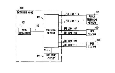
FIG. 1 shows a block diagram of a wireless telecommunication system.
Switch node 100 provides telecommunication switching service to wireless
handsets
that request such service via base stations 104 through 106. Node processor
101 via
bus 112 and network 102 and the appropriate BRI links provides control for the
base
stations. Switching network 102 provides switching between public telephone
network 105 and base stations 104 through 106. Each base station can have a
maximum of three active wireless handsets connected to it at any time. Each
BRI
link has two B channels for communicating a voice or data call. If base
station 104
is servicing three active wireless handsets, then three of the four B channels
in BRI
links 107 and 108 are in use. The fourth B channel of BRI links 107 and 108 is
always idle with respect to voice or data calls and is utilized to transmit
synchronization signals to base station 104 from DSP tone circuit 103 and
switching
network 102. These synchronization signals are transmitted from switching
network
102 to base stations 104 through 106 at the same instant of time. In addition
to
generating the synchronization signals, DSP tone circuit 103 generates all
other
tones required by switch node 100 such as dial tone or busy tone.
The synchronization signals generated by DSP tone circuit 103 is a
predefined repeating data pattern that is transmitted advantageously every
2.048
seconds: FIG. 3 illustrates the synchronization signals that are transmitted
to the
base stations. The connection through switching network 102 for the
synchronization signals from DSP tone circuit 103 via bus 113 are established
by
node processor 101 via control signals transmitted over bus 112 to switching
network 102.
FIG. 2 illustrates in greater detail the structure of switching network
102. Switching network 102 performs the switching of data and voice call's
utilizing
system TDM bus 201 and BRI TDM bus 202. Each TDM bus has 512 time slots that
repeat every 8kHz. Each PRI interface is connected to system TDM bus 201 via
its
own TSI such as TSI 205 and 206 for PRI interfaces 216 and 214, respectively.
The
time slot interchangers (TSI) 205-208 are utilized to transfer time slots from
one
TDM bus or PRI interface to another TDM bus or PRI interface. The control of
TSI
205-208 and the time slots utilized by BRI interfaces 209 through 213 and PRI
interfaces 214 through 216 is under control of network processor 204 which
receives
control information from node processor 101 via bus 112.
2 ~ ~~076
-4-
For example, consider the interconnection of a B channel on PRI link
114 being interconnected to a B channel on BRI link 107. BRI interface 209
places
data concerning the call on the specified B channel of BRI link 107 onto BRI
TDM
bus 202 in a specified time slot. TSI 208 is responsive to the data in the
specified
time slot to transfer continuously that data to system TDM bus 201 in a second
specified time slot on system TDM bus 201. TSI 206 is responsive to the second
specified time slot to transfer continuously that data to PRI interface 214 in
a third
specified time slot. PRI interface 214 is responsive to the data in this third
specified
time slot to transfer continuously that data on the specified B channel of PRI
link
114. The flow of data from PRI link 114 to BRI link 107 is similar.
DSP tone circuit 103 transmits tones and the synchronization signals in
individual time slots on link 113 to TSI 207. With respect to a tone such as
busy
tone, TSI 207 under control of network processor 204 may insert the data for
the
busy tone into a number of time slots on system TDM bus 201 depending upon the
number of B channels of BRI links on which the busy tone is to be transmitted.
However, the synchronization signals are inserted into only one specified time
slot
on system TDM bus 201 by TSI 207. TSI 208 is responsive to this specified time
slot on system TDM bus 201 to insert the synchronization signals into a second
specified time slot on BRI TDM bus 202. BRI interfaces 209 through 213 are
responsive to the synchronization signals in the second specified time slot on
BRI
TDM bus 202 to transmit this data on the fourth B channel of each of the BRI
interface pairs e.g., BRI interfaces 209 and 211. The synchronization signals
are
then utilized by each individual base station to synchronize the internal
clock of each
base station.
FIG. 3 illustrates synchronization pattern such as synchronization
signals 301-303. The synchronization pattern is repeated every 2.048 seconds.
Except during the synchronization signals, the data pattern sent by DSP tone
circuit
103 is an alternating one and zero pattern.
FIG. 4 illustrates base station 104 in greater detail. Microprocessor 401
in conjunction with ROM 403 and RAM 402 provide the overall control over the
base station. BRI interface 404 receives and transmits information on BRI
links 107
and 108. BRI interface 404 is responsible for information being communicated
with
switching network 102 of FIG. 1 on BRI links 107 and 108. BRI interface 404
communicates the two D channels via cable 421 with microprocessor 401 and
three
B channels with PCM to RF converter 406. Microprocessor 401 is responsive to
the
received information on the two D channels which is transferred to
microprocessor 401 via cable 422 to perform the required actions.
2188076
-5-
Microprocessor 401 communicates control information with BRI interface 404 via
cable 418 and PCM to RF converter 406 and RF circuit 407 via cable 417.
Converter 406 is communicating information between RF circuit 407 and BRI
interface 404. Converter 406 properly formats this information. In addition,
PCM to
RF converter 406 communicates control messages being transmitted by wireless
sets
received via RF circuit 407 to microprocessor 401.
Consider now the operation of pattern detection circuit 408 and divide
by 4,096 counter 409 in generating a 500 Hz phase synchronize pulse on
conductor 416 to RF circuit 407. Pattern detection circuit 408 receives via
conductor 410 from BRI interface 404 the frame strobe that indicates the start
of a
frame on the BRI links. This frame strobe occurs at a 8 KHz rate. In addition,
pattern detection circuit 408 receives the data being transmitted on the
dedicated B
channel from bus 412. Using this information, pattern detection circuit 408
detects
the synchronization signals 301, 302 through 303 illustrated in FIG. 3. Upon
detecting the synchronization signals, pattern detection circuit 408 transmits
a
counter clear signal on conductor 414 to reset counter 409. Counter 409 is
counting
at a rate of 2.048 MHz received from BRI interface 404 via conductor 413.
Counting at this rate, counter 409 generates a 500 Hz signal. The counter
clear
signal received via conductor 414 from pattern detection circuit 408 maintains
the
500 Hz signal in phase synchronization with the other base stations.
FIG. 5 illustrates in greater detail one possible embodiment of DSP tone
circuit 103. DSP 506 executes the program contained in dual port memory 502
using data also stored in memory 502 accessed via bus 508 to generate the
synchronization pattern and tones required by switch node 100. DSP 506 is
programmed using well known techniques to generate the synchronization pattern
and the tones. Board processor 501 determines the data and program that will
be
loaded into dual port memory 502. Board processor 501 is responsive to program
information received via bus 112 from node processor 101 of FIG. 1 to store
the
program utilized by DSP 506 in flash memory 504. In addition, board processor
501
stores its own program in flash memory 504. Flash memory 504 is utilized since
the
contents of flash memory 504 will not be lost in the event of a power failure.
RAM
memory 503 is utilized to hold the program and data utilized by board
processor 501
either for internal use or for transfer to dual port memory 502 for use by DSP
506.
As DSP 506 generates the tone and sync samples, these samples are transmitted
in
time slots on bus 113. As previously described, TSI 207 is responsive to each
time
slot to place that time slot in the specified time slot or time slots on
system TDM bus
201.