Note : Les descriptions sont présentées dans la langue officielle dans laquelle elles ont été soumises.
21929 ~
pLABMA CUTTING OR ARC WENDING POWER BUPPhY WITH
PHASE STAGGERED SECONDARY SWITCHERS
FIELD OF THE INVENTION
The invention relates generally to plasma arc
cutting and welding power supplies and more particularly to
a power supply with a plurality of secondary switchers.
BACKGROUND OF THE INVENTION
Plasma arc cutting is a process in which an
electric arc is used to cut a metallic workpiece.
Generally, plasma arc cutting uses an electric arc between
an electrode and the metal to be cut. The arc creates a
plasma that cuts the metallic workpiece.
It is generally accepted that approximately 250
volts (open circuit) is desirable to initiate a plasma arc
cutting process. After the process has been initiated, the
cutting arc voltage is approximately 90-125 volts. Of
course, the cutting arc (load output) voltage is dependent
upon the length of the cutting arc. The greater the length
of the arc, the greater the load voltage, and conversely,
2I9289i
-2-
the lesser the length of the arc the lesser the load
voltage. Similarly, the cutting arc voltage varies with the
magnitude of the output current.
A typical prior art plasma arc cutting power
supply receives an input voltage (from a power line or
generator) and provides an output voltage to a pair of
output terminals, one of which is the electrode and the
other of which is connected to the workpiece. The power
supplies provide about 250 volts open circuit and about
90-125 volts under load. There are numerous types of known
plasma arc cutting power supplies, such as magnetic power
supplies, inverter power supplies, phase control power
supplies, and choppers or secondary switchers. The present
invention relates to chopper based power supplies.
A typical prior art chopper shown in Figure 5
includes a voltage source 601, a switch 602, a diode 604 and
an inductor 603 which provide output current to load 605.
Voltage source 601 may be a transformer receiving line
voltage and a rectifier. Voltage source 601 should be
capable of providing input power, generally at a desired
voltage level. Of course, the source need not be a constant
_ voltage source but merely should be suitable for use with a
chopper power supply. When switch 602 is on current flows
from the positive output of voltage source 601 through load
605, inductor 603 and switch 602. During this time the load
current (and inductor current) is increasing and inductor
603 is storing energy, dependent upon the volt seconds
applied to inductor 603 while 602 is on. The volt seconds
are determined by the time switch 602 is on, and the source
and load voltages. When switch 602 is off current
freewheels through diode 604, load 605 and inductor 603.
While switch 602 is off the load current (and inductor
~~92~91
-3-
current) is decreasing and inductor 603 is returning energy,
again dependent upon the volt seconds (the time and load
voltage) induct~.r 603 applies to diode 604 and load 605. In
some high current applications a single voltage source may
have more than one chopper connected in parallel. The
choppers are operated in-phase with one another, thus the
load current is merely twice the output current of either
chopper.
The output voltage applied to load 605 is
dependent upon the duration of time switch 602 is on,
relative to the duration of time switch 602 is off.
Specifically, the output voltage is equal to the ratio of on
time of switch 602 to the on time plus off time of switch
602, multiplied by the output voltage of voltage source 601.
Thus, if switch 602 is on 50% of the time the load voltage
will be 50% of the source voltage. Typically, a current
feedback element is used in conjunction with a control
circuit to control the on and off time of switch 602.
Thus, a chopper will have a triangle (sawtooth)
current output having predetermined, but variable amplitude
or frequency according to the switching frequency. Their
operation is based on the controlled switching of a DC
voltage input to a desirable Dc current output. The
sawtooth output may be characterized as having a ripple
current, dependent on the maximum current less the minimum
current.
One drawback of chopper power supplies is the
ripple current rating of the output. When in-phase parallel
choppers are used, the output ripple is twice the ripple of
a single chopper. In a switching type (chopper) power
supply, the output cutting capability of the air plasma arc
cutter is adversely affected if its ripple current
2~92$~i
-4-
capability is not adequate for the job, i.e., cutting occurs
best at relatively constant current, not with a sawtooth
output. The life span of input capacitors in the voltage
source is also affected if the ripple current is greater
than the ratings. The ripple current generates internal
heat in the capacitor, with the attendant changes in
temperature dependent parameters. Elevated temperatures may
reduce the life expectancy of any electrochemical component.
It has often proved difficult to ensure a moderate ambient
l0 temperature for capacitors, much less to aggravate the
situation by permitting excessive ripple currents. Even
with an appropriately rated capacitor, dangerous internal
temperatures can develop when there is no provision for heat
removal from the external surface of the case.
Additionally, the magnitude of the peak current is dependent
upon the percent of ripple. Because high peak current can
erode consumables, a low ripple current is desirable.
Chopper power supplies, however, are relatively
inexpensive, controllable, and not lossy. Also, choppers
are well suited for receiving an input voltage, and provide
a load current at a lesser output voltage. Accordingly, it
is desirable to provide a chopper based power supply to take
advantage of the positive aspects of choppers, yet avoid a
major drawback -- excessive ripple current in the load.
Welding power supplies have many similarities to
plasma arc cutting power supplies. Specifically, the
welding process is best initiated with a generally accepted
fixed open circuit voltage (approximately 80 volts). After
initiation, however, the operating load output voltage is
generally in the range of 20-45 volts, and often 25 volts.
Finally, as in the plasma arc cutting process the actual arc
voltage varies with the current and the length of the arc.
2192891
-5-
In some welding applications it is desirable to have a
single power supply provide current to a number of welding
stations connected in parallel. Thus, more than one welder can
use a given power supply with this sort of arrangement.
Typically, to provide the necessary open circuit voltage to
initiate the welding arc the power supply will be a constant
voltage, 80 volts source. Each welding station includes a
variable resistor in series with the welding electrode (or
workpiece). The resistor dissipates sufficient power to provide
a typical load output voltage, 20 - 45 volts, e.g. As may be
readily seen this is very wasteful of power - as little as 25~
of the power is delivered to the arc load, while 75~ of the
power is dissipated in the resistor.
Accordingly, it is desirable to provide a welding
power supply that is capable of providing 80 volts open circuit
and in the range of 25 volts load voltage. Preferably, such a
welding power supply would be capable of providing multiple
parallel welding stations, without wasting power.
SUMMARY OF THE PRESENT INVENTION
According to one embodiment of the invention a power
supply, such as a plasma cutting power supply or a welding power
supply, provides an output to a pair of output terminals. The
power supply includes a source of voltage and a plurality of
choppers. The choppers are connected in parallel between the
voltage source and the output terminals. A controller controls
the choppers so that they are out-of-phase with respect to each
of the other of the plurality of choppers.
Preferably there are N choppers and the power supply
1
v.
2192891
-6-
provides an open circuit voltage (OCV) to the pair of output
terminals when no load is present and a load output voltage
(LOV) when a load is present. N is approximately equal to OCV/
LOV.
The choppers preferably include a freewheeling diode,
an inductor and a switch.
According to a second embodiment of the invention the
voltage source includes a transformer for receiving line voltage
and a rectifier.
According to a third aspect of the invention a user
selected current input is provided and current feedback is
provided. The control circuit receives the signals.
According to a third aspect of the invention there are
two choppers connected in parallel and the second chopper is
controlled substantially 180° out-of-phase with respect to the
first chopper.
According to a fourth aspect of the invention the
control circuit includes a ramp generator for generating a first
ramp signal for controlling the first chopper and a second ramp
signal for controlling the second chopper wherein the first ramp
signal is substantially 180° out-of-phase with respect to the
second ramp signal.
According to a fifth aspect of the invention there are
three choppers connected in parallel and the choppers are
controlled substantially 120° out-of-phase with respect to the
other choppers.
Other principal features and advantages of the
invention will become apparent to those skilled in the art upon
review of the following drawings, the detailed description and
the appended claims.
A
2192891
_,_
BRIEF DESCRIPTION OF THE DRAWINGS
Figure 1 is a block diagram of a power supply made
in accordance with the present invention;
Figure 2 is a circuit diagram of a chopper of
Figure 1 and a portion of the controller of Figure 1;
Figure 3 is a graph showing the current in each
chopper and the load current for a power_supply built in
accordance with the present invention used where the open
circuit voltage is approximately twice the load voltage;
Figure 4 is a graph showing the current in each
chopper and the load current for a power supply built in
accordance with the present invention used where the open
circuit voltage is approximately four times the load
voltage; and
Figure 5 is a circuit diagram of a prior art
chopper.
Before explaining at least one embodiment of the
invention in detail it is to be understood that the
invention is not limited in its application to the details
of construction and the arrangement of the components set
forth in the following description or illustrated in the
drawings. The invention is capable of other embodiments or
being practiced or carried out in various ways. Also, it is
to be understood that the phraseology and terminology
employed herein is for the purpose of description and should
not be regarded as limiting.
DETAILED DESCRIPTION OF THEPREFERRED EMBODIMENTS
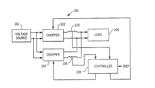
Generally, a plasma arc cutting power supply made
in accordance with the preferred embodiment is shown in
Figure 1. Plasma arc cutting power supply 100 includes a
chopper 102 and a chopper 104, connected in parallel. Both
2192891
_8_
choppers 102 and 104 receive an input voltage from a voltage
source 101. Chopper 102 includes an output current sensing
LEM 103 and chopper 104 includes an output current sensing
LEM 105. The choppers outputs are provided to a loaid 106.
A controller 108 receives a current feedback signal from
LEMs 103 and 105, as well as a current reference signal.
The current reference signal is a user_selected current
cutting magnitude and is typically provided by a
potentiometer on the front panel of the plasma arc cutting
power supply. Controller 108 provides a first switching
signal to chopper 104 and a second switching signal to
chopper 102. The switching signal determines when the
switches in choppers 102 and 104 turn on.
In accordance with the present invention, choppers
102 and 104 are operated out-of-phase with respect to one
another. Specifically, chopper 104 is operated 180°
out-of-phase with respect to chopper 102. As will be
described in greater detail below, this substantially
reduces the ripple output of power supply 100.
The arrangement of Figure 1 is of particular
usefulness in plasma arc cutting power supplies because of
the ratio of the desired open circuit voltage to the
approximate load voltage. Specifically, the ratio is close
to 2 (250 volts to 90-125 volts). Thus, if the voltage
source delivers a 250 volts open circuit, a load voltage of
approximately one-half that is obtained when each chopper is
on approximately 50% of the time.
In accordance with the present invention, when
each chopper is on 50% of the time, and out-of-phase 180°
with respect to the other chopper, the output ripple is
substantially zero. For example, as shown in Figure 3, a
chopper A output current and a chopper B output current are
2192891
_g_
shown for the switching times designated on and off
delineated by the dashed lines. The sum of these currents
is the current in the load any' may be seen to be
substantially flat.
In practice, the plasma arc cutting process
requires a load voltage of slightly less than one-half the
open circuit voltage, thus each chopper will be on somewhat
less than 50% of the time. Figure 4 shows the chopper
current and load current for a load output voltage of 25% of
the open circuit voltage. As may be seen the load output
current has a ripple (which is exaggerated for illustrative
purposes) that is approximately two-thirds that of the
ripple current in each chopper. Thus, a reduced ripple
output is provided.
Other applications may make use of a power supply
having parallel choppers out-of-phase with respect to one
another. Generally, the number of choppers should be
approximately equal to the ratio of the open circuit voltage
to typical load output voltage. Thus, for a welding power
supply having a desired open circuit voltage of 80 volts and
a load voltage of approximately 25 volts, three choppers in
parallel each 120° out-of-phase with respect to the other
two, would be appropriate.
Referring now to Figure 2, a preferred embodiment
of part of controller 108 and chopper 102 is shown.
Controller 108 includes a ramp generator 201, a current
error circuit 203 and a drive circuit 205. Controller 108
may include other components and portions typical in the
art.
Ramp generator 201 includes a plurality of op amps
A3A, A3B and A3C. Op amp A3A is configured as an integrator
and includes a feedback capacitor C12 connected to the
2192891
-10-
inverting input. The noninverting input of op amp A3A is
connected to ground. The output of op amp A3A is provided
through a.-resistor R44 to inverting op amp A3B. Op amp A3B
includes a feedback resistor R52 connected to its inverting
input and the noninverting input connected to ground. The
output of op amp A3B is directly connected to the inverting
input of op amp A3C which is configured as a comparator. -Op
amp A3C includes feedback resistors R50 and R51 connected to
the noninverting input of op amp A3C. The output of A3C is
provided through a resistor R45 as an input to the
noninverting input of op amp A3A.
Thus, ramp generator 201 generates a sawtooth ramp
at the output of A3A, through a resistor R34 (the signal is
labeled RAMP A). The output of op amp A3B is RAMP B and is
identical to RAMP A except that it is 180° out-of-phase with
respect to RAMP A. RAMP B is provided through a resistor
R53 to current error circuit 203. RAMP A and RAMP B are the
timing signals used to determine the length of the off time
plus on time of the switches in choppers 102 and 104.
Current error circuit 203 includes an input IFB,
which is a current feedback signal derived from an LEM, such
as LEM 103 on the output of chopper 102. The signal may be
processed in a manner typical in the art. Current error
circuit 203 also includes an IREF input, which is the user
selected desired current (typically obtained using a single
potentiometer on the front panel of the power supply).
The signal representative of the user selected
current, IREF, is provided through a pair of resistors R8
and R69 to amplifier op amp A2A. The current feedback
signal, IFB, is provided through resistor R38 to amplifier
A2A. Both the current reference signal and the current
feedback signal are provided to the inverting input of op
2192891
-11-
amp A2A. The noninverting input of op amp A2A is connected
to ground. A negative 15 volts signal is also connected to
the inverting input of amplifier A2A through resistor R37,
to provide a minimum current bias.
Amplifier A2A includes feedback resistors R18,
R19, C1, diodes D1 and D2 connected from its output to its
inverting input. The output of amplifier A2A is thus a
current error signal, i.e., representative of the difference
between the reference current and the feedback current. The
minimum bias current signal is provided through resistor R37
to provide a minimum current. when IREF is at its minimum
level.
The output of amplifier A2A is provided through a
resistor R30 to the inverting input of op amp A2B. Op amp
A2B is connected as a comparator and receives as a timing
input RAMP B, from ramp generator 201, on its noninverting
input. Thus, the output of comparator A2B is a "one" or
"zero," depending upon whether the current error signal from
R30 is greater or less than the timing signal (RAMP B).
The output of comparator A2B is provided through a
resistor R36 to an inverter UlA. The output of inverter UlA
is provided to a gate driver circuit 205. The output of
inverter UlA controls, through gate driver circuit 205, when
the switch in chopper 102 is on and off, dependent upon the
timing signal RAMP B generated by ramp generator 201 and the
difference between the current reference signal and the
current feedback signal.
Gate driver circuit 205 includes totem pole
MOSFETS, Q4 and Q5. The totem pole MOSFETS Q4 and Q5 are
driven by the output of inverter UlA, provided through a
resistor R46 and capacitor C16 to create a delay. The
output of capacitor C16 is provided to an inverter U1B,
2192891
-12-
which drives the gate of MOSFET Q4. A diode is provided
across resistor R46. Similarly, resistor R47, diode D10,
capacitor C13 and inverter U1C are provided as inputs to the
gate of transistor Q5. The RC networks R46 and C16, and R47
and C13, provide a small delay before the turning on of
either MOSFET Q4 or MOSFET Q5. Diodes D9 and D10 provide
for the instantaneous turning off of the MOSFETS Q4 and Q5.
Thus, a crowbar across MOSFETS Q4 and Q5 is avoided.
MOSFETS Q4 and Q5 are connected between a positive
15 volts source and ground. The node common to MOSFETS Q4
and Q5 is provided through a resistor R32 to chopper 102,
and turns the switch in chopper 102 on and off. Resistor
R32 limits the charge current into the gate of the switch in
chopper 102. A resistor R31 is provided to hold the IGBT
off when the machine power is off. An electrolytic
capacitor C9 and a decoupling capacitor C8 are provided
between the positive 15 volts power supply and ground:
As shown on Figure 2, chopper 102 includes an IGBT
Q6 (or some other switch) which receives the gate driver
signal. Freewheeling diodes D16 and an inductor L2 are
provided in a standard chopper configuration. Resistor R21,
a diode D14 and a capacitor C7 provide a snubber for IGBT
Q6. LEM 103 is shown also, and outputs, 207 and 208, are
shown.
When the difference between IREF and IFB indicates
additional current is needed, IGBT Q6 will stay on for a
longer portion of time, thus providing additional volt
seconds and allowing the current in inductor L2 and the load
to rise to a greater magnitude. When less current is
needed, indicated by IFB being greater than IREF, IGBT Q6
will be turned on for a lesser portion of time. Thus, the
control of chopper 102 has been described.
- 2192891
-13-
Chopper 104 is cpntrolled using circuitry
identical to current error circuit 203 and gate driver
circuit 205. However, the ramp input to the current error
circuit of chopper 104 is RAMP A, not RAMP B. Thus, the
output of the current error circuit that controls chopper
104 is substantially that of current error signal 203, but
180° out-of-phase. The gate driver circuit for chopper 104
(not shown) is identical to that of gate driver circuit 205.
The output of the gate driver circuit (not shown) is
provided to chopper 104.
Thus, as may be seen, choppers 102 and 104 are
controlled to be 180° out-of-phase with respect to one
another. Additionally, choppers 102 and 104 are controlled
to provide a desired current to load 106.
The above preferred embodiment has been described
with respect to a plasma arc cutting power supply, but will
work equally well with a welding power supply. More
particularly, for a welding power supply it would be
desirable to provide approximately three choppers in
parallel because the open circuit voltage is often
approximately three times the output load voltage.
When a welding power supply is made in accordance
with this invention, it is well suited for having multiple
welding stations (connected in parallel). Each station
would include three choppers, 120° out-of-phase with respect
to the other two choppers. Such a power supply will have
less ripple than a standard chopper, and less power loss
than the prior art resistor based welding stations.
Thus, it should be apparent that there has been
provided in accordance with the present invention a power
supply with phase staggered secondary switchers that fully
satisfies the objectives and advantages set forth above.
2192891
-14-
Although the invention has been described in conjunction
with. specific embodiments thereof, it is evident that many
alternatives, modifications and variations will be apparent
to those skilled in the art. Accordingly, it is intended to
embrace all such alternatives, modifications and variations
that fall within the spirit and broad scope of the appended
claims.
2192891
-15-
REFERENCE NO. COMPONENT TYPE VALUE
A2A Linear 347 Op-Amp
A2B Linear 347 Op-Amp
A3A Linear 347 Op-Amp
A3B Linear 347 Op-Amp
A3C Linear 347 Op-amp
C1 Capacitor 0.01 micro F
C7 Capacitor 0.01 micro F
C12 Capacitor 0.001 micro F
C13 Capacitor 100 pico F
C16 Capacitor 100 pico F
C9 Electrolytic 10 micro F
Capacitor
C8 Capacitor 1 micro F
C35 Capacitor 0.1 micro F
C39 Capacitor O.l.micro F
Dl Zener Diode 7.5 volt
D2 Diode
D9 Diode
D14 Diode
D16 Diode
L2 Inductor
LEM 1 Current Transducer
Q4 P Channel MOSFET
Q5 N Channel MOSFET
Q6 IGBT
R30 Resistor 10 K Ohm
R31 Resistor 10 K Ohm
R34 Resistor 10 K Ohm
2192891
-16-
REFERENCE NO. COMPONENT TYPE QALUE
R36 Resistor 10 K Ohm
R50 Resistor 10 K Ohm
R53 Resistor 10 K Ohm
R19 Resistor 15 K Ohm
R45 Resistor 15 K Ohm
R51 Resistor 5.11 K Ohm
R18 Resistor 2.74 M Ohm
R8 Resistor 30.1 K Ohm
R37 Resistor 30.1 K Ohm
R21 Resistor 1 K Ohm
R38 Resistor 8.25 K Ohm
R32 Resistor 15 Ohm
R44 Resistor 100 K Ohm
R52 Resistor 100 K Ohm
R46 Resistor 12.1 K Ohm
R47 Resistor 12.1 K Ohm
R54 Resistor 274 Ohm
R69 Resistor 2.21 K Ohm
UlA 40106 Inverter
U1B 40106 Inverter
U1C 40106 Inverter