Sélection de la langue

Search

Sommaire du brevet 2199214 

Énoncé de désistement de responsabilité concernant l'information provenant de tiers

Une partie des informations de ce site Web a été fournie par des sources externes. Le gouvernement du Canada n'assume aucune responsabilité concernant la précision, l'actualité ou la fiabilité des informations fournies par les sources externes. Les utilisateurs qui désirent employer cette information devraient consulter directement la source des informations. Le contenu fourni par les sources externes n'est pas assujetti aux exigences sur les langues officielles, la protection des renseignements personnels et l'accessibilité.

Disponibilité de l'Abrégé et des Revendications

L'apparition de différences dans le texte et l'image des Revendications et de l'Abrégé dépend du moment auquel le document est publié. Les textes des Revendications et de l'Abrégé sont affichés :

  • lorsque la demande peut être examinée par le public;
  • lorsque le brevet est émis (délivrance).
(12) Brevet: (11) CA 2199214
(54) Titre français: DISPOSITIF DE COMMUTATION ENTRE UNE SOURCE D'ALIMENTATION EXTERNE ET UNE SOURCE D'ALIMENTATION PAR PILE PRINCIPALE
(54) Titre anglais: EXTERNAL POWER SOURCE TO MAIN BATTERY POWER SOURCE SWITCH
Statut: Réputé périmé
Données bibliographiques
(51) Classification internationale des brevets (CIB):
  • H02J 9/06 (2006.01)
  • H02J 9/00 (2006.01)
  • H03K 17/30 (2006.01)
  • H04B 1/44 (2006.01)
  • H04M 1/00 (2006.01)
  • H04M 1/02 (2006.01)
  • H04Q 7/32 (2006.01)
(72) Inventeurs :
  • BARKAT, SHAKIL H. (Etats-Unis d'Amérique)
  • BLACK, GREGORY REDMOND (Etats-Unis d'Amérique)
(73) Titulaires :
  • MOTOROLA, INC. (Etats-Unis d'Amérique)
(71) Demandeurs :
  • MOTOROLA, INC. (Etats-Unis d'Amérique)
(74) Agent: GOWLING WLG (CANADA) LLP
(74) Co-agent:
(45) Délivré: 2000-05-16
(22) Date de dépôt: 1997-03-05
(41) Mise à la disponibilité du public: 1997-09-13
Requête d'examen: 1997-03-05
Licence disponible: S.O.
(25) Langue des documents déposés: Anglais

Traité de coopération en matière de brevets (PCT): Non

(30) Données de priorité de la demande:
Numéro de la demande Pays / territoire Date
08/614,604 Etats-Unis d'Amérique 1996-03-13

Abrégés

Abrégé français

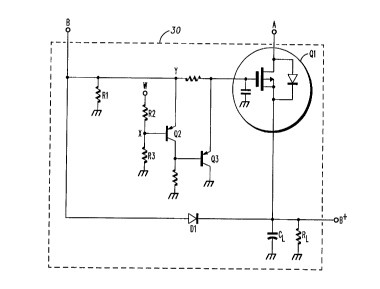
Circuit de commutation (30), dans un téléphone portatif, appliquant à une grille de transistor à effet de champ (Q1) une tension inférieure à la tension de seuil de la grille lorsque la tension à une première borne d'alimentation (B) tombe sous une valeur de seuil, ce qui a pour effet de couper la connexion entre la première borne d'alimentation (B) et une borne d'entrée d'alimentation du téléphone portatif (B+) et de raccorder une deuxième borne d'alimentation (A) à la borne d'entrée d'alimentation (B+). La tension de seuil est établie à un niveau supérieur à la tension d'alimentation minimale du téléphone portatif. La première borne d'alimentation peut être connectée à une pile principale et la deuxième borne d'alimentation peut être connectée à un adaptateur, p. ex. adaptateur de simulateur de pile, adaptateur mains-libres ou adaptateur d'émetteur-récepteur mobile. Le présent circuit de commutation empêche un appel en cours d'être coupé lorsque les sources d'alimentation sont changées pendant une rafale GSM.


Abrégé anglais


A switching circuit (30) in a portable telephone connects a gate of a
field-effect transistor (Q1) to a voltage below the transistor's gate threshold
voltage when the voltage at a first power source terminal (B) falls below a
threshold voltage, thus disconnecting the first power source terminal (B)
from a portable telephone power input terminal (B+) and connecting a
second power source terminal (A) to the power input terminal (B+). The
threshold voltage is set at a voltage above the minimum supply voltage of
the portable telephone. The first power source terminal may be connected
to a main battery and the second power source terminal may be connected
to an adapter such as a battery eliminator adapter, hands-free adapter, or
mobile transceiver adapter. This switching circuit prevents a call in
progress from being disconnected when power sources are exchanged
during a GSM burst.

Revendications

Note : Les revendications sont présentées dans la langue officielle dans laquelle elles ont été soumises.


CLAIMS:

1. A power source switching circuit for a portable telephone having a minimum
supply voltage comprising:
a first power source terminal;
a second power source terminal;
a portable telephone power input terminal;
a field-effect transistor having a gate threshold voltage for switchably
connecting either the first power source terminal or the second power source
terminal
to the portable telephone power input terminal; and
a circuit for switching a gate of the field-effect transistor below the gate
threshold voltage when a voltage at the first power source terminal falls to a
threshold
voltage that is at least equal to the minimum supply voltage.

2. A power source switching circuit according to claim 1 wherein a first power
source connected to the first power source terminal is an external power
source.

3. A power source switching circuit according to claim 1 wherein a second
power
source connected to the second power source terminal is a portable battery.

4. A power source switching circuit according to claim 1 wherein the circuit
switches the gate of the field-effect transistor above the gate threshold
voltage when a
voltage at the first power source terminal rises to the threshold voltage.

5. A power source switching circuit according to claim 4 wherein a first power
source connected to the first power source terminal is an external power
source.

6. A power source switching circuit according to claim 4 wherein a second
power
source connected to the second power source terminal is a portable battery.

6


7. A power source switching circuit according to claim 1 wherein the circuit
comprises:
a first transistor having a predetermined base-emitter junction potential
connected to the first power source terminal; and
a second transistor having a base connected to a collector of the first
transistor.

8. A power source switching circuit according to claim 7 wherein the
predetermined base-emitter junction potential of the first transistor is at
least equal to
the minimum supply voltage.

9. A power source switching circuit according to claim 1 further comprising a
diode connected to the first power source terminal and the portable telephone
power
input terminal.

10. A power source switching circuit according to claim 9 wherein the
threshold
voltage is at least equal to the minimum supply voltage plus a diode drop
voltage
across the diode.

11. A method for switching power sources of a portable telephone having a
minimum supply voltage comprising the steps of:
detecting when a voltage at a first power source terminal falls below a
threshold voltage that is at least equal to the minimum supply voltage;
connecting a gate of a field-effect transistor having a gate threshold voltage
to
a voltage lower than the gate threshold voltage; and
using the field-effect transistor to disconnect the first power source
terminal
from a portable telephone power input terminal and connect a second power
source
terminal to the portable telephone power input terminal.

12. A method for switching power sources according to claim 11 wherein the
threshold voltage is at least equal to the minimum supply voltage plus a diode
drop
voltage.


7


13. A method for switching power sources according to claim 11 wherein the
step
of connecting further comprises:
turning off a first transistor having a predetermined base-emitter junction
potential connected to the first power source terminal; and
turning on a second transistor having a base connected to a collector of the
first transistor.
14. A method for switching power sources according to claim 13 wherein the
predetermined base-emitter junction potential of the first transistor is at
least equal to
the minimum supply voltage.
15. A method for switching power sources according to claim 13 wherein the
threshold voltage is at least equal to the predetermined base-emitter junction
potential
of the first transistor plus a voltage drop across the first transistor.
16. A power source switch for a portable telephone having a minimum supply
voltage comprising:
means for switching a portable telephone power input terminal connection
from a first power source terminal to a second power source terminal when a
voltage
at the first power source terminal falls below a threshold voltage; and
means for setting the threshold voltage to be at least equal to the minimum
supply voltage in order to maintain a call in progress.


8

Description

Note : Les descriptions sont présentées dans la langue officielle dans laquelle elles ont été soumises.


. - . '
CE01906R-Barkat et al.
EXTERNAL POWER SOURCE TO
MAIN BATTERY POWER SOURCE SWITCH
Field of the Invention
This invention relates generally to radio-telephones, and more
particularly to a portable telephone that can accommodate a power source
change during a telephone call on a Global System for Mobile
Communications platform.
B_ack~round of the Invention
Portable telephones currently use batteries as their main power
source. For example, cellular telephones use an attached or internal
portable battery, and transportable telephones, sometimes called bag-
phones, use a portable battery. Adapters, such as battery eliminator
adapters; hands-free adapters, or mobile transceiver adapters, can be
connected to a vehicle cigarette lighter to provide an external power source
for augmenting the main battery. Switching from the main battery to the
external power source and vice versa interrupts the power supply to the
telephone and may cause termination of a cellular telephone call in
process under certain conditions. For example, Global System for Mobile
Communications (GSM) applications incorporate a burst mode that pulls
1.6 A or more during a burst. If the cellular telephone power supply is
changed during a GSM burst, a telephone call in process may be
terminated abruptly due to a failure to complete the power source switch-
over during a limited switching period.
The switching period can be lengthened by using a capacitor as a
charge storage device. Currently, a large 3300 ~,F capacitor with dimensions
of 48 mm by 12 mm stores a charge during the switch-over. As portable
telephones reduce in size, however, incorporating a large capacitor into a
telephone is undesirable. Thus, there is a need for a portable telephone
1


CA 02199214 1999-11-22
that accommodates a power source change during a telephone call without
requiring a large capacitor.
Sub
A switching circuit enables a portable telephone to change from a main
battery power source to an external power source, such as a vehicle battery,
and
vice versa during a telephone call without a risk of forced call termination.
A
switching circuit drives a field-effect transistor (FET) to switch immediately
to
a second power source before the voltage at a first power source terminal
drops
below the minimum supply voltage required to keep the telephone turned on.
Thus, this switching circuit enables the telephone to switch between various
power sources without dropping a call in progress. Switching from a main
portable battery to an external power source occurs most often when a portable
telephone is connected to an adapter such as a battery-eliminator adapter,
hands-free adapter, or mobile transceiver adapter, which is in turned powered
by a vehicle battery.
Switching from an external power source to a main portable battery
occurs most often when the vehicle ignition is switched off.
Incorporating this switching circuit into a portable telephone eliminates
the need for a large capacitor as a charge storage device, which reduces the
size
and weight of the portable telephone.
30 la


CA 02199214 1999-11-22
~.E01906R-Barkat et al.
Brief Description of the Drawings
FIG. 1 shows prior art switching circuit.
FIG. 2 shows a graph of voltage at terminals A, B, and B+ during a
power source substitution.
FIG. 3 shows a power source switching circuit according to a
preferred embodiment.
Detailed Description of the Invention
A switching circuit enables a portable telephone to change from a
main battery power source to an external power source, such as a vehicle
battery, and vice versa during a telephone call without a risk of forced call
termination. A switching circuit drives a field-effect transistor (FET) to
switch immediately to a second power source before the voltage at a first
power source terminal drops below the minimum supply voltage required
to keep the telephone turned on. Thus, this switching circuit enables the
telephone to switch between various power sources without dropping a
call in progress. Switching from a main portable battery to an external
power source occurs most often when a portable telephone is connected to
an adapter such as a battery-eliminator adapter, hands-free adapter, or
mobile transceiver adapter, which is in turned powered by a vehicle
battery. Switching from an external power source to a main portable
battery occurs most often when the vehicle ignition is switched off.
Incorporating this switching circuit into a portable telephone eliminates
the need for a large capacitor as a charge storage device, which reduces the
size and weight of the portable telephone.
FIG. 1 shows prior art switching circuit. In this circuit, main battery
power source terminal A is connected to portable telephone power input
terminal B+ through FET Ql, which includes an inherent diode and
2


' ~ ~ ~ ~ ~ ~ ~ ~ CE01906R-Barkat et al.
capacitor. External power source terminal B is connected to the gate of FET
Q1 with pull-down resistor R1. Diode D1, which is preferably a Schottky
diode, connects terminal B to power input terminal B+. When external
power is available at terminal B, the voltage of the external power source
is greater than the voltage of the main battery power source, therefore the
gate of FET Q1 is high and power from the external power source is
supplied to the telephone.
When external power is removed from terminal B, the voltage at
the gate of FET Q1 drops and main battery power at terminal A is
connected to the telephone power input terminal B+ once the gate of FET
Q1 drops below the FET gate threshold voltage. The time it takes for the
gate of FET Q1 to go low is determined by the amount of time it takes to
discharge the inherent capacitance in the FET through resistor R1. This
switch must take place before capacitor CL fully discharges through load
resistor RL. If the voltage at input terminal B+ drops below a threshold
voltage, the telephone will turn off and any call in progress will be
dropped. Thus, if the charge stored in capacitor CL is not large enough at
the time of the switch-over, the FET will not switch during the short
capacitor discharge period, and a telephone call in progress will be
dropped. This occurs most commonly when the power sources are
exchanged during a GSM burst.
FIG. 2 shows a graph of voltage at terminals A, B, and B+ during a
power source substitution. Plot 21 shows the voltage at power input
terminal B+ during a GSM burst 211 lasting approximately 550 sec. Plot 22
shows the voltage at external power source terminal B, which in this
example is the first power source. Plot 23 shows the voltage at main battery
terminal A, which in this example is the second power source. Note the
bounce that occurs when the second power source is inserted. If the power
sources are exchanged during a burst 212, the gate of FET Q1 does not drop
quickly enough to switch to the second power source before the power at
input terminal B+ dips below the minimum supply or shut-off voltage of
the portable telephone. The minimum supply voltage is shown at 2.85
volts, thus a call in progress would terminate at point 25.
3


' ~ ~ ~ ~ CE01906R-Barkat et al.
Increasing the capacitance of capacitor CL provides additional charge
at input terminal B+ during a power source exchange and increases the
time available for FET Q1 to perform a switch, however, the physical size
of the capacitor required to ensure that a call is not dropped during a
power source exchange during a GSM burst is undesirably large.
FIG. 3 shows a power source switch according to a preferred
embodiment. Switching circuit 30 eliminates the need for a bulky high-
capacitance capacitor to prohibit the undesired turn-off of a telephone
during a power source substitution. The voltage at node W is supplied
from a linear regulator powered from input terminal B+. Resistors R2 and
R3 are chosen so that the voltage at node X is preferably at least the
minimum supply voltage of the telephone. The voltage at node Y would
then be approximately 0.7 volts above the voltage at node X. When the
voltage at terminal B drops below the threshold voltage at node Y,
transistor Q2 turns off and transistor Q3 turns on, connecting the gate of
FET Q1 to ground or any other voltage below the gate threshold voltage of
FET Q1. Thus, switching circuit 30 forces the FET Q1 to switch over at a
faster rate and eliminates the need for a large capacitance at capacitor CL.
With a 20 ~,F capacitor CL, the FET Q1 has approximately 11.4 ~l,sec to switch
from the first power source to the second power source, which is more
then enough time to complete the switch-over given switching circuit 30.
Conversely, when the external power source is reconnected and the
voltage at terminal B exceeds the threshold voltage at node Y, transistor Q2
turns on and transistor Q3 turns off.
The voltage at node X can be set lower than the turn-off voltage of
the portable telephone, however, the threshold voltage at node Y should
be at least the turn-off voltage of the telephone plus the voltage across
diode D1. For example, if diode D1 is a Schottky diode with a 0.4 volt drop
and the minimum supply voltage of the telephone is set at 2.65 volts, the
minimum threshold voltage at node Y is 3.05 volts. Thus, the switching
circuit 30 eliminates the voltage drop point 25 shown in FIG. 2.
Thus, the switching circuit 30 prevents the telephone from
disconnecting a call in progress even if the power source is changed during
4


' ' 219 ~ 2 I 4 CE01906R-Barkat et al.
a GSM burst. The external power source to main battery power source
switch eliminates the need for a large capacitor yet maintains cellular
telephone calls in progress during a power source substitution. While
specific components and features of the switching circuit are described
above, modified components or features could be employed by one skilled
in the art within the true spirit and scope of the present invention. The
invention should be limited only by the appended claims.
5

Dessin représentatif
Une figure unique qui représente un dessin illustrant l'invention.
États administratifs

Pour une meilleure compréhension de l'état de la demande ou brevet qui figure sur cette page, la rubrique Mise en garde , et les descriptions de Brevet , États administratifs , Taxes périodiques et Historique des paiements devraient être consultées.

États administratifs

Titre Date
Date de délivrance prévu 2000-05-16
(22) Dépôt 1997-03-05
Requête d'examen 1997-03-05
(41) Mise à la disponibilité du public 1997-09-13
(45) Délivré 2000-05-16
Réputé périmé 2005-03-07

Historique d'abandonnement

Il n'y a pas d'historique d'abandonnement

Historique des paiements

Type de taxes Anniversaire Échéance Montant payé Date payée
Requête d'examen 400,00 $ 1997-03-05
Enregistrement de documents 100,00 $ 1997-03-05
Le dépôt d'une demande de brevet 300,00 $ 1997-03-05
Taxe de maintien en état - Demande - nouvelle loi 2 1999-03-05 100,00 $ 1998-12-22
Taxe de maintien en état - Demande - nouvelle loi 3 2000-03-06 100,00 $ 1999-12-16
Taxe finale 300,00 $ 2000-02-21
Taxe de maintien en état - brevet - nouvelle loi 4 2001-03-05 100,00 $ 2001-02-19
Taxe de maintien en état - brevet - nouvelle loi 5 2002-03-05 150,00 $ 2002-02-04
Taxe de maintien en état - brevet - nouvelle loi 6 2003-03-05 150,00 $ 2003-02-04
Titulaires au dossier

Les titulaires actuels et antérieures au dossier sont affichés en ordre alphabétique.

Titulaires actuels au dossier
MOTOROLA, INC.
Titulaires antérieures au dossier
BARKAT, SHAKIL H.
BLACK, GREGORY REDMOND
Les propriétaires antérieurs qui ne figurent pas dans la liste des « Propriétaires au dossier » apparaîtront dans d'autres documents au dossier.
Documents

Pour visionner les fichiers sélectionnés, entrer le code reCAPTCHA :


Pour visualiser une image, cliquer sur un lien dans la colonne description du document. Pour télécharger l'image (les images), cliquer l'une ou plusieurs cases à cocher dans la première colonne et ensuite cliquer sur le bouton "Télécharger sélection en format PDF (archive Zip)" ou le bouton "Télécharger sélection (en un fichier PDF fusionné)".

Liste des documents de brevet publiés et non publiés sur la BDBC .

Si vous avez des difficultés à accéder au contenu, veuillez communiquer avec le Centre de services à la clientèle au 1-866-997-1936, ou envoyer un courriel au Centre de service à la clientèle de l'OPIC.


Description du
Document 
Date
(yyyy-mm-dd) 
Nombre de pages   Taille de l'image (Ko) 
Description 1997-03-05 5 223
Revendications 1997-03-05 3 65
Dessins 1997-03-05 2 25
Revendications 1999-11-22 3 111
Description 1999-11-22 6 256
Page couverture 2000-05-09 2 64
Abrégé 1997-03-05 1 27
Dessins représentatifs 1997-10-20 1 5
Dessins représentatifs 2000-05-09 1 5
Page couverture 1997-10-20 2 62
Cession 1997-03-05 9 304
Poursuite-Amendment 1999-07-21 2 5
Poursuite-Amendment 1999-11-22 10 328
Correspondance 2000-02-21 1 26