Note : Les descriptions sont présentées dans la langue officielle dans laquelle elles ont été soumises.
. ~ 2199948
SELF-ALIGNED FIELD-EFFECT TRANSISTOR
FOR HIGH FREQUENCY APPLICATIONS
Field of the Invention
The present invention relates to field-effect
transistors ("FETs") in wide bandgap materials, and
particularly relates to a self-aligned metal-
semiconductor field-effect transistor (MESFET)
structure formed in silicon carbide that provides
advantages in high frequency operation.
Background of the Invention
The metal-semiconductor field-effect
transistor is one of a family of field-effect devices,
the three main types of field-effect transistors being
junction field-effect transistors (JFETs), metal-
oxygen-semiconductor field-effect transistors
(MOSFETs), and MESFETs.
As known to those familiar with semiconductor
devices, JFETs and MESFETs operate identically to one
another, the difference being that a MESFET uses a
metal-semiconductor rectifying contact for the gate
electrode instead of a p-n junction. Each of these
structures offer certain processing and performance
advantages. For MESFETS, these advantages potentially
include low temperature formation of the gate structure
(as compared to the generally more sophisticated
formation of p-n junctions), low resistance and low
. ~ 2 199949
-2-
current-resistance ("IR") drop along the channel width,
and good heat dissipation for power devices.
Alternatively, a MESFET's metal contact structure is
more susceptible to leakage current, particularly at
high,temperatures, so that JFETs can often operate at
higher temperatures than MESFETS.
As just noted, the general theory and
operations of JFETs and MESFETs are well understood.
An illustrative discussion is set forth, for example,
in Chapter 6 of Sze, Physics of Semiconductor Devices,
2nd Edition (1981)
Metal-semiconductor field-effect transistors
are particularly useful for high frequency
applications. Such applications include electrical
1S circuits requiring high power handling capability
(greater than 20 watts) while operating a high
frequencies such as radio frequencies (500 megahertz),
S-band frequencies (3 gigahertz), and X-band
frequencies (10 gigahertz), the use of which has become
more prevalent in recent years. Because of the
increase in high power, high frequency circuits, demand
has correspondingly increased for transistors capable
of operating reliably at radio and higher frequencies
while still handling higher power loads. Previously,
bipolar transistors and power MOSFETs have been used
for high power applications, but the power handling
capability of such devices is generally limited at
higher operating frequencies.
The MESFET structure is preferred for high
frequency applications because only the majority
carriers carry current. The MESFET design is also
preferred over current MOSFET designs because the
reduced gate capacities permit faster switching of the
gate input. Therefore, although all field-effect
transistors utilize only majority carriers to carry
current, a MESFET's Schottky gate structure makes the
MESFET more desirable for high frequency applications.
2199948
= ~
-3-
in addition to the device structure, the
characteristics of the semiconductor material from
which a transistor is formed also affect the operating
parameters. Such semiconductor characteristics include
electron mobility, saturated electron drift velocity,
electric breakdown field, and thermal conductivity.
For many years, most high frequency MESFETs
have been manufactured of n-type III-V compounds such
as gallium arsenide (GaAs) because of their high
electron mobilities. Although these devices provided
increased operating frequencies and moderately
increased power handling capability, their relatively
low breakdown voltage and their lower thermal
conductivity have limited their usefulness in high
power applications.
Silicon carbide (SiC) has been known for many
years to possess excellent physical and electronic
properties which theoretically should provide the basis
for electronic devices that can operate at higher
temperatures, and higher power at high frequencies than
devices produced from silicon or gallium arsenide.
Silicon carbide has an electric breakdown field of
about 4x10⁶ volts per centimeter, a saturated electron
drift velocity of about 2.0x10⁷ centimeters per second,
and a high thermal conductivity of about 4.9 watts per
centimeter-Kelvin, all of which makes silicon carbide
suitable for high frequency, high power applications.
Silicon carbide is notoriously difficult to
work with, however, particularly because of the high
processing temperatures required to grow it, its
physical hardness, and its characteristic
crystallization in approximately 150 polytypes, most of
whigh are separated by relatively small thermodynamic
differences.
More recently, however, progress in silicon
carbide research has provided the practical success in
device manufacture to match silicon carbide's
CA 02199948 2004-11-12
-4-
theoretical potential. In particular, U.S. Patent No.
5,270,554 and Canadian Patent No. 1,312,148, disclose
successful MESFETs in silicon carbide. Both of these
patents represent developments carried out by the
assignee of the present invention. The 1554 U.S. patent
is assigned to the present assignee, and the 1148
Canadian patent is exclusively licensed to the present
assignee.
Additionally, interest is increasing in other
wide bandgap semiconductor materials such as Group III
nitrides (i.e., Group III of the periodic table),
including binary compounds such as gallium nitride (GaN),
and ternary and quaternary nitrides such as GaAlN and
InGaAlN.
In seeking improvements in these devices,
careful evaluation of their properties has shown that
much of the source and drain resistance in MESFETs formed
in silicon carbide results from the physical gap between
the ohmic contact metal layer and the gate contact. More
specifically, recent careful analysis of existing devices
has revealed that approximately half of the source
resistance of current silicon carbide MESFETs results
from this gap.
As is known to those familiar with present
manufacturing techniques for semiconductor devices, this
gap is on the order of about 1 micron. This represents
the current smallest tolerance that can be achieved using
the masking and etching steps by which semiconductor
devices of all types, including those formed in silicon
carbide, are typically formed. Thus, although a
tolerance as small as 1 micron is generally considered to
be excellent in many respects, it has now
2 199948
-5-
been discovered that this very small gap contributes
significantly to the source resistance of the device.
As known to those familiar with semiconductor
devices and particularly JFETs and MESFETs, the
increased source resistance in turn lowers the
potential gain and power efficiency of a MESFET at
microwave frequencies. Perhaps most fundamentally, the
increased source resistance also lowers the maximum
operating frequency, Finax=
There thus exists the need to reduce the
source resistance in JFETs and MESFETs formed in
silicon carbide and Group III nitrides in a manner
which will increase their gain, their efficiency, and
their maximum operating frequencies.
Object and Summary of the Invention
Therefore, it is an object of the present
invention to provide a field effect transistor with
reduced source resistance and a corresponding increase
in gain, power efficiency, and F,,,a,.
The invention meets these objects with a
metal-semiconductor field-effect transistor (MESFET)
that comprises an epitaxial layer of silicon carbide
having a first conductivity type. A gate trench in the
epitaxial layer exposes the silicon carbide gate
surface between two respective trench edges, and the
trench further defines the source and the drain regions
of the transistor. A rectifying gate contact is on the
gate surface, and respective ohmic metal layers form
ohmic contacts on the source and drain regions of the
epitaxial layer. The edges of these ohmic metal layers
at the trench are specifically aligned withthe edges
of the trench in the epitaxial layer.
In another aspect, the invention comprises a
method of forming such a self-aligned metal-
semiconductor field-effect transistor in silicon
carbide.
CA 02199948 2005-11-04
- 5a -
According to an aspect of the invention, there is provided a field-
effect-transistor (FET) that exhibits reduced source resistance and higher
operating
frequencies, said FET comprising:
an epitaxial layer of silicon carbide having a first conductivity type;
a gate trench in said silicon carbide epitaxial layer that defines the
surface of the gate region of the FET between two respective trench edges,
said trench
further defining the boundaries of the source and drain regions of said
transistor;
a metal contact on said gate surface for biasing a rectifying gate
junction at said gate surface; and
respective ohmic metal layers forming ohmic contacts on said source
and drain regions of said epitaxial layer;
wherein said metal layers have respective edges at the edge of said
trench, said edges of said metal layers at said trench being specifically
aligned with
said edges of said epitaxial layer at said trench for eliminating the
additional source
resistance caused when the respective edges of said epitaxial layer and said
metal
layers are not aligned.
According to another aspect of the invention, there is provided, a
method of forming a self aligned field-effect-transistor (FET) in silicon
carbide that
exhibits reduced source and drain resistance and higher operating frequencies,
the
method comprising:
depositing an ohmic contact metal layer on an epitaxial layer of silicon
carbide in a pattern that defines a gate trench location at which the
epitaxial layer is
exposed between portions of the ohmic contact metal layer;
etching a gate trench through the epitaxial layer of silicon carbide; and
forming a gate junction to the epitaxial layer at the bottom of the
trench;
wherein the etching step comprises an etchant and process that do not
remove the ohmic contact metal layer so that the metal layer effectively masks
portions of the silicon carbide epitaxial layer to thereby self-align the
edges of the
metal and the edges of the silicon carbide layer at the trench.
CA 02199948 2005-11-04
- 5b -
According to a further aspect of the invention, there is provided A
metal-semiconductor field-effect-transistor (MESFET) that exhibits reduced
source
resistance and higher operating frequencies, said MESFET comprising:
a substrate;
an n-type Group III nitride epitaxial layer on said substrate;
a gate trench in said epitaxial layer that exposes a gate surface between
two respective trench edges, and said trench further defining the source and
drain
regions of said transistor;
a rectifying Schottky gate contact to said gate surface; and
respective ohmic metal layers forming ohmic contacts on said source
and drain regions of said epitaxial layer;
wherein said metal layers have respective edges at the edge of said
trench, said edges of said metal layers at said trench being specifically
aligned with
said edges of said epitaxial layer at said trench for eliminating the
additional source
resistance caused when the respective edges of said epitaxial layer and said
metal
layers are not aligned.
2199948
-6-
The foregoing and other objects, advantages
and features of the invention, and the manner in which
the same are accomplished, will become more.readily
apparent upon consideration of the following detailed
description of the invention taken in conjunction with
the accompanying drawings, which illustrate preferred
and exemplary embodiments, and wherein:
Figure 1 is a cross-sectional view of a prior
art MESFET;
Figure 2 is a cross-sectional view of a
MESFET according to the present invention;
Figure 3 is a schematic top plan view of a
masking pattern according to the method of the
invention;
Figure 4 is a cross-sectional view of a JFET
according to the present invention.
Detailed Description
Figure 1 is a representation of a typical
MESFET formed in silicon carbide and broadly designated
at 10. The device 10 includes a silicon carbide
substrate 11, and an epitaxial layer of silicon carbide
illustrated in Figure 1 in two portions as the channel
layer 12 and the cap layer 13. It will be understood,
however, that a single layer could suffice. In typical
MESFETs, both the channel layer 12 and the cap layer 13
are usually n-type conductivity. The gate contact is
illustrated at 14 and is positioned in the trench
broadly designated at 15 formed in the cap layer 13.
In order to provide ohmic contact to the
source and drain regions, a metal suitable for an ohmic
contact is deposited on the cap layer and is designated
as portions 16 and 17 to distinguish the source portion
16 from the drain portion 17. Typically, an
interconnect metal shown as the portions 20 (for the
source) and 21 (for the drain) complete the device
structure.
~N 2 199948
-7-
As is known to those familiar with the
manufacture of such devices, a typical method for
building the device of Figure 1 is to first grow the
epitaxial cap layer 13 on the channel layer 12. The
gate trench 15 is next etched, after which the
structure is masked and the ohmic metal (nickel or a
nickel alloy being typical examples for silicon
carbide) is deposited to make the ohmic contacts. The
physical limitations of working in such small
dimensions are such that it has been difficult to date
to align the mask for the metal any closer to the
trench than about 1 micron. As a result, a source gap
designated at 22 and a drain gap designated at 23 are
present on the cap layer 13 between the edge of the
respective metal portions 16 and 17 and the edges of
the gate trench 15.
As foreshadowed earlier, it has now been
discovered that although a FET's source resistance is a
product of several factors, the largest factor--one
which contributes approximately half of the source
resistance--is this gap 22 along the cap layer 13
between the ohmic contacts 16 and the trench 15.
The invention eliminates this gap 22 and thus
eliminates approximately half of the source resistance.
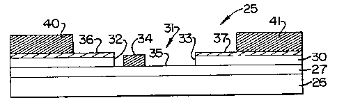
Figure 2 illustrates the structure of the
invention and shows a MESFET broadly designated at 25.
The invention is preferably supported by a silicon
carbide substrate 26. Those familiar with wide bandgap
materials and devices will recognize, however, that
devices such as this have been formed on other
substrate materials such as sapphire, silicon, or even
diamond, and thus the invention encompasses=.such
substrates. Silicon carbide is preferred, however,
because it can provide an exact lattice match with the
silicon carbide epitaxial layers to be grown upon it.
An epitaxial layer of silicon carbide having
a first conductivity type is formed on the epitaxial
2 199949
-8-
layer 26. In the preferred embodiment of the
invention, and as illustrated in Figure 2, the
epitaxial layer is formed of a channel layer 27 and a
cap layer 30, both having n-type conductivity. As
noted earlier, a single epitaxial layer could suffice.
The epitaxial layer has a gate trench broadly
designated at 31 that exposes a silicon carbide gate
surface between two respective trench edges 32 and 33.
The trench thus further defines the source and drain
regions of the transistor. A rectifying gate contact
34 is made to the gate surface 35 to define the gate
region of the transistor, and respective ohmic metal
layers 36 and 37 form ohmic contacts on the source and
drain regions of the cap epitaxial layer 30. As
illustrated by Figure 2, the edges of the metal layers
36 and 37 are specifically aligned with the edges 32
and 33 of the trench 31 in the epitaxial layer 30.
Interconnect metal portions 40 and 41 are also shown in
Figure 2 and, providing they are compatible with the
ohmic contact metal layers 36 and 37, can be selected
in an appropriate manner from a number of high
conductivity metals well known in this art, including
gold (Au), silver (Ag), aluminum (Al), and copper (Cu).
As for the ohmic contact metal layers 36 and
37, an appropriate contact material is qualified
functionally as one that provides ohmic behavior with
the semiconductor, and one that doesn't react
unfavorably with the etchant. For a FET in silicon
carbide, the ohmic contact preferably comprises a
nickel (Ni) alloy that is formed by depositing nickel
on the SiC surface and then annealing it. As-deposited
aluminum (Al) will also form an ohmic conta.ct to SiC.
Similarly, the gate contact can be selected
from the group consisting of gold, platinum (Pt),
platinum silicide, and titanium, and in a preferred
embodiment comprises platinum. In preferred
embodiments, a gold overlay covers the platinum gate
~ 2199948
-9-
contact, and successive layers of titanium, platinum,
and gold overlay the annealled nickel ohmic contacts.
As well known to those familiar with the
crystal structure advantages of semiconductor devices,
the.substrate 26, the channel layer 27, and the cap
layer 30 are all preferably formed of the same polytype
of silicon carbide, and these are generally selected
from the group consisting of the 3C, 2H, 4H, GH, and
15R polytypes of silicon carbide, with the
understanding that bulk single crystal substrates of 3C
silicon carbide are generally more difficult to form.
In the Group III nitride embodiments of the
device, the substrate can be silicon carbide, and if a
buffer layer of aluminum nitride (not shown) is
included between the substrate and the FET structure,
the silicon carbide substrate can be n or p-type, semi-
insulating, or even substantially undoped. Sapphire is
an appropriate alternative substrate material, and is
insulating in character.
In order to enhance the operation of the
device, the cap layer 30 typically has a higher carrier
concentration than the channel layer 27, and both are
generally formed of n-type silicon carbide.
As further known to those familiar with
MESFET operation, the substrate 26 is preferably semi-
insulating in character, although it can also have the
opposite conductivity type from the epitaxial layers 27
and 30. Thus, when the epitaxial layers are preferably
n-type, the substrate will be either semi-insulating or
p-type. In yet other embodiments, a p-type, semi-
insulating, or even substantially undoped epitaxial
layer (not shown) can provide a buffer between the
substrate and the FET so that the conductivity of the
substrate does not affect the performance of the
remainder of the structure; i.e.; can be n-type, p-
type, or semi-insulating.
2 199948
-10-
As Figure 2 illustrates, because the-edges of
the ohmic contact layers 36 and 37 are aligned with the
edges 32 and 33 of the trench 31, the gaps shown at 22
and 23 in Figure 1 are eliminated, thus immediately
eliminating approximately fifty percent of the source
resistance in the transistor.
Figure 4 is a cross-sectional view of a
junction field-effect transistor (JFET) according to
the present invention. As in the MESFET embodiment
illustrated in Figure 2, the JFET of Figure 4, broadly
designated at 45, includes a substrate 46, a channel
epitaxial layer 47, and a cap epitaxial layer 50. A
trench 51 is formed in the cap layer 50 and includes a
gate contact 52 which can be of an appropriate ohmic
metal;,rather than a Schottky metal. In the embodiment
shown in Figure 4, a p-n junction is formed by an
implanted well 53 of p-type material in the n-type
channel layer 47 prior to adding the gate contact 52.
As in the previous embodiments, the ohmic contact
metals 54 and 55 respectively are aligned with the
edges 56 and 57 of the trench 51. Interconnect metals
60 and 61 complete the structure.
In another aspect, the invention comprises a
method of forming the self-aligned metal-semiconductor
field-effect transistor of the present invention. The
first step comprises depositing an ohmic contact metal
layer on an epitaxial layer of silicon carbide in a
pattern that defines a gate trench location at which
the epitaxial layer is exposed between portions of the
ohmic contact metal layer.
The second step comprises etching a gate
trench through the epitaxial layer.of silicon carbide
with an etchant and process that do not remove the
ohmic contact metal layer. As a result, the metal
layer effectively masks portions of the silicon carbide
epitaxial layer to thereby self-align the edges of the
metal and the edges of the trench in the silicon
2 199948
-11-
carbide layer to form the source and drain regions. A
gate contact is then applied to the epitaxial layer at
the bottom of the trench.
In sequential fashion, the method can further
comprise the step of forming the epitaxial layer of
silicon carbide supported by a silicon carbide
substrate prior to the step of depositing the layer of
ohmic contact metal. In turn, the step of forming an
epitaxial layer can comprise the steps of forming an
epitaxial channel layer of silicon carbide on the
substrate, and then forming an epitaxial cap layer of
silicon carbide on the epitaxial channel layer of
silicon carbide.
The method can further comprise masking a
portion of the ohmic contact layer prior to the step of
etching the gate trench to thereby provide portions of
the ohmic contact layer that are unaffected by the etch
and thus more suitable for providing further
interconnecting source and drain contacts to the ohmic
contact layer. Figure 3 illustrates such a masking
pattern in which the ohmic contact metal layers 36 and
37 identically corresponding to the same reference
numerals in Figure 3 are shown as having portions
schematically covered by the masks 42 and 43
respectively. Although typical etchants for silicon
carbide do not usually remove annealed nickel and some
other metals, the etchants will often tend to react to
some degree with the metal surface and make it less
suitable for further electrical contact. Thus, by
masking a portion of the nickel during the etching
step, a better surface is preserved for later adding
the interconnect metal.
As in the structural embodiments, the step of
depositing the ohmic contact metal preferably comprise
depositing nickel and then annealing it. The step of
applying a gate contact comprises applying a gate
contact selected from the group consisting of gold,
2 199948
-12-
platinum, platinum silicide and titanium, and
preferably platinum. Typical interconnect metals are
selected for their high conductivity, and include gold,
silver, aluminum, and copper.
In yet another embodiment of the invention,
and using an etchant and process that will etch both
silicon carbide and the ohmic contact metal (or a first
etchant for the metal and a second etchant for the
silicon carbide), the method can comprise etching a
gate trench through the ohmic contact metal layer
covering the epitaxial layer of silicon carbide and
also through the silicon carbide layer to thereby self-
align the edges of the metal and the edges of the
trench in the silicon carbide layer. The gate contact
is then applied to the epitaxial layer at the bottom of
the trench as previously described.
The various process steps described herein
can be carried out using techniques developed by the
assignee of this invention. The growth of silicon
carbide epitaxial layers of various types on various
substrates are set forth in U.S. Patent Nos. 4,912,063;
4,912,064; and 5,011,549, all of which are incorporated
entirely herein by reference. The etching step can be
carried out in accordance with the teachings of U.S.
Patent Nos. 4,865,685 and 4,981,551, the contents of
which are incorporated entirely herein by reference.
If desired, surface preparation can be carried out in
accordance with U.S. Patent Nos. 4,946,547 and
5,200,022, the contents of both of which are
incorporated entirely herein by reference. Finally, if
ion implantation is used to form any of the layers or
junctions described herein, it can be carried out using
the,techniques described in U.S. Patent No. 5,087,576,
the contents of which are likewise incorporated
entirely herein by reference.
In the drawings and specification, there have
been disclosed typical preferred embodiments of the
2199948
-13-
invention and, although specific terms have been
employed, they have been used in a generic and
descriptive sense only and not for purposes of
limitation, the scope of the invention being set forth
in the following claims.