Note : Les descriptions sont présentées dans la langue officielle dans laquelle elles ont été soumises.
'" CA 02203947 2000-08-03
TV'~O TERMINAL ACTIVE ARC SUPPRESSOR
Technical Field
This invention relates generally to arc suppressor circuits for
electrical contacts and more specifically concerns such a circuit which
includes a
power transistor, such as an IGBT, connected in parallel with the electrical
contacts
being protected, wherein the protective circuit can be used with a wide
variety of
electrical contact arrangements.
Backaround of the Invention
As indicated in co-pending Canadian patent application Serial No.
2,185,051 laid open for public inspection on March 13, 1997, a common problem
with electrical contacts, i.~.. the mechanical contacts used in electric or
electromechanical circuits, through which current flows when the contacts are
closed, is the creation of an electrical arc between the contacts as they
begin to
open from a closed position. -this can occur as contacts open, either if the
contacts
are normally closed or norm~~lly open. If the voltage across the contacts as
they
open reaches a sufficient levol, an arc will form between the contacts.
Further, this
arc may continue even after i:he contacts are well open. This arcing is well
known
to be undesirable because of the wear it produces on the contacts as well as
other
circuit effects which may occur due to the arc.
In addition to the design of the contacts themselves, which in some
cases provide an inherent arc suppression capability, separate arc suppression
circuits have been used to prE:vent arcing across electrical contacts. These
circuits
typically include a power transistor with particular operating
characteristics. The
initial increase in the voltage across the electrical contacts as the contacts
open
is used as an activating sil~nal to turn the power transistor on, momentarily
shunting the load current an~und the contacts during the time the contacts are
opening. Typically, this is accomplished through the use of Miller capacitance
connected to the transistor vvith the current though the Miller capacitance
being
sufficient to momentarily turn the power transistor on.
One such cir~;uit is shown in U.S. Patent No. 4,438,472 to
Woodworth. Woodworth teaches the basic idea of using a shunting capacitor in
CA 02203947 1999-12-10
-2-
combination with a bipolar junction transistor. In this particular
implementation, the
additional Miller capacitance must be relatively large. This large
capacitance,
however, remains in parallel with the contacts being protected even when they
are
fully open, acting in effect as a short circuit relative to any transients
which may be
impressed across the contacts. This of course is undesirable in many
situations.
Further, the bipolar junction transistor must be capable of handling the
energy from
the inductive load as it (the transistor) gradually interrupts the load
current.
Another implementation is shown in U.S. Patent No. 4,658,320 to
Hongel. In Hongel, the bipolar junction transistor is replaced with a power
field
effect transistor (FET). This does have the effect of reducing the size of the
large
capacitance required by the Woodworth apparatus. However, as with the
Woodworth apparatus, the gradual inductive load current interruption requires
that
virtually all of the load energy be dissipated in the FET itself. An FET
capable of
handling this is expensive, and is fairly large in size. In addition, the
capacitor in
Hongel still parallels the open contacts, so that it is susceptible to
transient
voltages.
The apparatus described in the '051 patent application, which is
owned by the assignee of the present invention, overcomes many of the
disadvantages of the above two circuits. It reduces the necessary Miller
capacitance and is designed to prevent electrical conduction through the
protective
circuit during voltage transients. However, that apparatus was designed to be
used with a particular electrical contact arrangement, known generally as a
form
C contact. In the '051 circuit, the unused portion of the form C contact was
used
to~signal the shunting power transistor when to shut off and to hold that
transistor
off even in the presence of large voltage transients.
The present invention has all of the advantages of the '051 circuit,
but is not limited to a particular contact arrangement. Indeed, it can be used
with
basically any type of electrical contacts where arcing is a problem, and can
be
readily designed to operate in a number of different circuit arrangements. Not
only
can a wide variety of electrical contacts be covered, but various contact
separation
rates can also be accommodated. Hence, the present invention is quite general
in its applicability.
CA 02203947 1999-12-10
-3-
Summary of the Invention
Accordingly, the invention is a circuitforsuppression of arcing across
electrical contacts, comprising: a power transistor, such as an IGBT,
connected
across the contacts; capacitance means, connected between the contacts and the
power transistor but not directly across the contacts, sufficient that the
power
transistor quickly turns on when the contacts begin to open, providing a
current
path around the contacts, thereby preventing arcing across the contacts; means
for turning off the power transistor following sufficient separation of the
contacts to
prevent arcing thereacross; and voltage limiting means to limit any flyback
voltage
resulting from the power transistor turning off to a selected level.
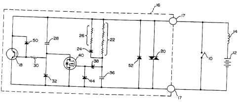
Brief Description of the Drawings
Figure 1 is a diagram showing one embodiment of the arc
suppression circuit of the present invention.
-_ _ __-. _ __._ _ _ .
CA 02203947 1997-04-29
4
Figure 2 is an alternative embodiment of the
arc suppression circuit of the present invention.
Figure 3 is a diagram showing one example of
an electrical voltage transient.
Figure 4 shows a simplified electrical
representation of the transient source relative to the
circuit of the present invention.
Best Mode for Carrvina Out the Invention
The arc suppression circuit of the present
invention, one embodiment of which is shown in Figure 1,
is designed to operate with a wide variety of electrical
and/or electromechanical contacts. The electrical
contacts, for purposes of illustration, are shown
generally at 10. The battery 12 represents a source of
voltage operating through a load 14, which in the
embodiment shown is a combination of inductance and
resistance. The source voltage produces a current
through load 14 and through the contacts 10. The arc
suppression (protective) circuit of the present
invention is shown generally at 16, connected to
contacts l0 at connection points 17-17. Arc suppression
circuit 16 includes in the embodiment shown a power
transistor i8 which in the embodiment shown is an
Insulated Gate Bipolar Junction Transistor (IGBT). An
IGBT is a Darlington-type combination of a field effect
transistor (FET) and a bipolar junction transistor (BJT)
capable of handling high power levels.
In general, arc suppression circuit 16 is
connected in parallel with contacts 10, such that IGBT
18 shunts the electrical contacts. The load current is
briefly shunted around the contacts through the
protective circuit as the contacts open, until the
contacts have separated sufficiently that they can
withstand the source voltage, typically several hundred
volts. After contacts 10 have separated, IGBT 18 is
quickly and abruptly turned off; the ensuing inductive
CA 02203947 1997-04-29
voltage kick or flyback is limited or clamped by a
voltage limiting device, such as a metal oxide varistor
(MOV) shown in Figure 1 at 20. In the embodiment of
Figure 1, the voltage limiting device 20 is internal to
5 the circuit, while in an alternative embodiment, the
voltage limiting device is external and may be supplied
by the user of the circuit. In that embodiment, the
voltage clamping characteristics may be adapted by the
user to the particular load and the particular contacts
used.
As indicated briefly above, arc suppression
circuit 16 can be used with electrical contacts which
are normally closed or normally open. In either case,
when the contacts open after having been closed with
current flowing therethrough, arc suppression circuit 16
operates to prevent an arc from appearing across the
electrical contacts. For purposes of explanation of the
operation of circuit 16, it will be assumed that
contacts 10 are normally closed and that load current is
flowing from the positive terminal of voltage source 12
through load 14, through contacts 10 and back to source
12.
As contacts 10 begin to open in response to an
electrical control signal or manual operation of a
switch, load current through the contacts will terminate
and the current will begin to flow in the arc
suppression circuit. IGBT 18 will not immediately
conduct the current, since it is an off condition.
Further, the voltage across contacts 10 is not
sufficient to break down the voltage limiting element
20, nor will substantial current flow through combined
resistance 22. In addition, because of diode 24, no
current will flow through combined resistance 26. This
results in current eventually passing through capacitor
28, which is the Miller capacitance, and then through a
gate resistor 30, the gate-emitter capacitance of the
IGBT 18, and then back to the voltage source 12.
CA 02203947 1997-04-29
6
The current established through this path of
capacitor 28 and resistor 30 and the gate-emitter
capacitance of the IGBT 18 results in both of the
capacitances beginning to charge. IGBT 18 will begin to
conduct when its gate-to-emitter capacitance charges
past its threshold voltage. Capacitor 28 has such a
size (for example, 2.2 nanofarads) that the charge which
is necessary at the gate of the IGBT to turn it on
results in a voltage on capacitor 28 which is small
compared to the voltage on the IGBT.
At this point, the voltage across both the arc
suppression circuit 16 (i.e. across connection points
17-17) and electrical contacts 10 is limited
approximately to the threshold voltage of IGBT 18. As
the voltage increases further, more current flows
through capacitor 28 and through the gate-emitter
portion of IGBT 18, turning on IGBT harder, which limits
the voltage increase. At this point, the overall
circuit would appear to be in balance; further voltage
rise at the gate of the IGBT is limited by this current
balance condition. However, any delay in IGBT 18
turning on could result in a destructively high voltage
being developed at the gate of the IGBT, which might
typically be 20 volts. Zener diode 32 ensures that the
voltage on the gate of the IGBT is limited to a value
which is below the danger level, while resistance 30
tends to prevent oscillations in IGBT operation.
When IGBT 18 begins to conduct, the voltage
developed across arc suppression circuit 16 results in
a current flow through resistance 22, charging capacitor
36. When the voltage on capacitor 36 exceeds the
reverse breakover voltage of zener diode 38, diode 38
begins to conduct, turning on transistor 40, which in
the embodiment shown is an FET. The voltage level
across the protective circuit 16 is established by the
characteristics of IGBT 18 and the value of Miller
capacitor 28.
CA 02203947 1997-04-29
7
The turn-on time of FET 40 is controlled by
the time constant established by resistance 22 and
capacitor 36. The value of resistance 22 also controls
the amount of leakage current for the suppression
circuit, which might for example be 150 microamps.
The time from the initial separation of
contacts 10 to the conduction of zener diode 38 is
determined and then established by selecting an
appropriate value for capacitor 36. This time delay can
be readily matched to the separation rate for the
particular contacts being protected. As an example, one
millisecond will typically be a safe value, as most
contacts separate a sufficient distance to withstand the
source voltage in less than one millisecond.
When FET 40 turns on, a path is provided for
the discharge of the gate-to-emitter capacitance of IGBT
18. This discharge path includes resistor 30, FET 40
and then back to the emitter of IGBT 18. Once the
capacitance is discharged thorough this path, IGBT 18
turns off. This early abrupt turnoff of the IGBT 18
after it has been turned on saves or preserves the IGBT.
Since the contacts 10 are still opening (or in
some cases completely open) and the IGBT is turned off,
the inductive load current is forced to flow through the
voltage limiting device, such as an MOV, shown generally
at 20.
The voltage across MOV 20, arc suppression
current 16 and contacts 10 increases to the clamping
voltage level of MOV 20, typically a few hundred volts.
The increase in voltage results in additional current
from source voltage 12 through Miller capacitance 36 and
FET 40. The additional current, however, because FET 40
is conducting, does not result in IGBT 18 turning back
on. Further, because the clamping voltage of MOV 20 is
higher than the source voltage 12, a negative voltage is
developed across load 14. This negative voltage causes
a decrease in the inductive load current flow; shortly
CA 02203947 1997-04-29
a
thereafter, the inductive load current decreases to
zero.
Since current is also now flowing through
resistor 22, capacitor 36 will continue to charge. When
capacitor 36 has charged, this will result in the gate
source capacitance of FET 40 charging, through zener
diode 38. When this charge reaches the breakover
voltage of zener diode 44, zener 44 begins to conduct,
limiting the gate-to-source voltage of FET 40 to a safe
(non-destructive) level.
Since FET 40 is not required to carry
significant DC current or hold off a substantial level
of voltage, it can be selected such that the amount of
charge which must be on its gate-source capacitance to
turn on FET 40 is relatively small. Accordingly, arc
suppression circuit 16 need only supply a relatively
small amount of current through zener 38, for only a
short time, to turn FET 40 on. Accordingly, FET 40
turns on quite rapidly after current begins to flow in
circuit 16; hence, IGBT 18 turns off rapidly as well,
since FET 40 controls the turn-off of IGBT 18. This
prompt and abrupt turnoff of IGBT 18 results in
basically all of the load current flowing through MOV
20.
Hence, since load current actually flows
through IGBT 18 for only a relatively short time, and is
quite promptly and abruptly interrupted, the energy
which must be dissipated in IGBT 18 is relatively small
compared to the total energy which must be dissipated to
successfully interrupt the load current. This results
in the size and cost of the IGBT being significantly
reduced relative to predecessor circuits, such as
discussed above. MOV 20, on the other hand, dissipates
large amounts of energy, but this is acceptable, since
an MOV having such a capability is still relatively
inexpensive.
CA 02203947 1997-04-29
9
After a time, contacts 10 may close again, due
to either manual action or an electrical control signal.
When the contacts 10 close, it is important at that
point that the arc suppression circuit be brought back
to its original operating state (i.e. re-arm) as quickly
as possible so that it can accommodate an early
reopening. This is particularly necessary in the
situation where the contacts may open unintentionally
very soon after initially being closed, such as occurs
in the case of "contact bounce".
When contacts l0 close, the voltage across the
protecti-~e circuit 16 falls to zero, resulting in
capacitor 36 discharging through diode 24 and resistance
26. This occurs because resistance 26 is selected to be
significantly smaller than resistance 22. This
discharge current flows back through contacts 10 to
capacitor 36. The gate-to-source capacitance of FET 40
will also discharge through zener diode 38, diode 24,
resistance 26 and contacts 10, back to FET 40. This
results in FET 40 turning off.
Further, the Miller capacitance 28 will
discharge through contacts 10, and zener diode 32.
Zener diode 32 prevents this discharge current from
developing a destructive negative voltage across the
gate-to-emitter portion of IGBT 18. Still further, the
gate to emitter capacitance of IGBT 18 will discharge
through diode 50 and contacts 10.
The fast discharge of capacitors 36 and 28,
and the internal capacitance of FET 40 and IGBT 18 will
thus quickly return arc suppression circuit 16 to its
original condition. This action in effect "re-arms" the
protective circuit, so that it is ready for the next
opening of contacts l0. Because these capacitances, and
resistor 26, are capable of rapidly discharging the
capacitances of the protective circuit, the circuit will
return to its original state very quickly. As indicated
briefly above, this fast re-arming protects contacts to
CA 02203947 1997-04-29
to
from destructive arcing during "contact bounces"
following closing of the contacts.
In the event that arc suppression circuit 16
is inadvertently connected backwards at 17-17, diode 52
will limit the negative voltage presented to the arc
suppression circuit, protecting the semiconductors in
the circuit from destructive voltage levels, until the
connection error is realized.
As indicated above, one of the advantages of
the circuit of the present invention is its protection
against voltage transients. After contacts 10 have
opened and the load current through the contacts is at
zero, the voltage across protective circuit 16 is equal
to the source voltage, i.e., if the source voltage for
the load is a 125-volt battery, the voltage across
contacts 10 and the protective circuit 16 is also 125
volts DC. As discussed above, the presence of this
voltage results in current flow through resistance 22,
zener diode 38 and zener diode 44, which holds FET 40
on, which in turn holds IGBT 18 off. This is the
"balanced" condition of the circuit after the contacts
have been open for a short time. A positive voltage
transient which may occur thereafter across the open
contacts 10 will, in the circuit shown, result in
current flowing through Miller capacitance 28, to the
drain connection of FET 40. However, the value of
resistor 30, and the on-resistance of FET 40 are
selected so that the majority of the current will flow
through the FET on-resistance. Hence, a positive
voltage transient will not result in IGBT turning on.
This provides protection against false triggers of the
IGBT due to positive voltage transients.
The circuit of Figure 1 also protects against
oscillating transients, i.e. those transients which
comprise alternating positive and negative excursions
which decrease in amplitude, either quickly, or over
several periods of oscillation. It is important for the
CA 02203947 1997-04-29
11
protective circuit 16 to hold off such transients
without allowing load current to flow from the source
voltage through the load. Oscillatory transients
present some difficulty because the negative going
excursions may be difficult to distinguish from actual
closing of contacts 10, since both of those events cause
the voltage across arc suppression circuit 16 to rapidly
fall.
If arc suppression circuit 16 misinterprets
the negative portion of an oscillatory transient as a
closing of the contacts, then the ensuing positive
excursion will likely activate protective circuit 16 and
allow current to flow from the voltage source through
the load. An example of an oscillatory transient 59 is
shown in Figure 3. The source of the transient, as
shown in Figure 4, is a transient generator 60 with
source impedance 62, applied across the arc suppression
(protective) circuit 16. The source voltage, load and
contacts are shown at 12, 14 and 10, respectively.
During the negative portion of the oscillatory
transient 59, diode 52 (Figure 1) provides a low
impedance path for the resulting current, effectively
clipping the negative portion of the voltage transient
to about zero volts; the entire transient voltage
(negative portion) is thus dropped across the transient
source impedance 62.
During the positive portion of the voltage
transient 59, diode 52 presents a high impedance to the
positive voltage. Any current which flows through the
Miller capacitance 36 during this portion of the voltage
transient is, as explained above, diverted away from
IGBT 18 by FET 40. Hence, IGBT remains off. Any
voltage across contacts 10 is allowed to rise until that
voltage reaches the breakover voltage of MOV 20. When
MOV 20 begins to conduct, it presents a low impedance
path for the transient current, so that the high voltage
CA 02203947 1997-04-29
12
transient is clipped, because most of the voltage is
dropped again across source impedance 62.
Thus, the action of diode 59 clips the
negative portion of the voltage transient to
substantially zero volts, while MOV 20 clips the
positive portion of the voltage transient to
approximately its breakover voltage, which as an example
may be a few hundred volts. The result is an asymmetry --
in the oscillatory waveform, producing an average DC
offset or bias. This offset DC voltage tends to charge
capacitor 36 more during the positive portion of the
transient than to discharge it during the negative
portion. Thus, the positive portion tends to maintain
FET 40 on, more than the negative portion tends to turn
it off. FET 40 thus remains on during the entire
transient, which results in IGBT 18 being held off
during the same transient, thereby preventing false
triggering of IGBT 18.
The particular operation of FET 40 in response
to oscillatory transients results in the fact that FET
40 is allowed to turn off faster than it is allowed to
turn on during normal operation. This provides
additional protection against arcing during the very
quick contact bounce subsequent to initial closing of
the contacts. Diodes 24 and 38 and resistance 26 are
selected so that the gate-to-source capacitance of FET
40 and capacitor 28 discharge much faster than the
values of resistance 22 and zener 38 allow capacitor 36
and the gate-to-source capacitance of FET 40 to charge.
Basically, this is due to resistance 26 being selected
to be much smaller than resistance 22. Since FET 40
turns off quickly, capacitor 28 and IGBT 18 protect
contacts 10 from arcing during bounces.
Even with the above-described protection
against various transients, it is possible that IGBT 18
might turn on in response to a charge which for a
variety of undetermined reasons occurs directly on the
CA 02203947 1997-04-29
13
gate-to-emitter capacitance of IGBT 18. Further, if the
charge is sufficient to result in IGBT 18 turning on to
full conduction, and in addition there is insufficient
voltage across protective circuit 16 to properly and
quickly operate the IGBT turn-off circuitry comprised of
resistance 22, capacitor 36, zener diode 38 and FET 40.
Thus, it is possible that the IGBT 18 could continue in
full conduction, limited only by leakage currents and/or
the action of parasitic capacitors; this is an
undesirable condition. However, this possibility is
effectively prevented by diode 50 which is connected
between the gate and collector of IGBT 18.
Since IGBT 18 has an inherent gate-to-emitter
threshold voltage below which it will not conduct, and
since diode 50 effectively clamps the collector thereof
to a voltage which is at least one diode drop below the
threshold voltage, diode 50 effectively prevents the
collector-to-emitter voltage from IGBT 18 from dropping
below the gate threshold voltage of IGBT 18. This
ensures that regardless of how IGBT 18 turns on, there
remains sufficient voltage across the protective circuit
16 to operate the IGBT turnoff circuitry, comprised of
resistor 22, capacitor 36, diode 38 and FET 40.
As indicated above, in the circuit of Figure
1, element 18 is a power transistor. An IGBT satisfies
the operational requirements of the circuit and the
above description. An example of such an IGBT is
IRGBC30S, manufactured by International Rectifier.
Other possibilities besides an IGBT could include a
power FET. Transistor 40, identified as a field effect
transistor in the preferred embodiment, produces a rapid
turnoff of IGBT 18, which minimizes the size and cost of
IGBT 18. Element 40 could be various fast action
devices, including various FETs, a silicone bilateral
switch, a unijunction transistor, or a standard
thyristor triggered by a zener diode. Further, the
inherent positive feedback of the protective circuit 16
CA 02203947 1997-04-29
14
itself can be used for the turnoff of IGBT 18. Figure
2 shows such an alternative circuit.
In the arrangement of Figure 2, diode 70 is a
zener diode. Resistance 22 and the zener diode 38 from
the circuit of Figure 1 have been eliminated. A
resistor 72 is in parallel with zener diode 74. In
operation, when contacts 76 open, the load current is
shunted around the contacts, developing a voltage across --
the arc suppression (protective) circuit 75. This is
basically similar to the circuit of Figure 1. The
voltage across protective circuit 75 increases slowly,
due to the current flow in resistor 72, which allows
capacitor 80 to charge, which in turn results in the
collector-to-gate voltage of the power transistor (IGBT)
82 to increase.
The voltage across contacts 76 also will
gradually increase until that voltage reaches the
breakover voltage of diode 70. At this point, diode 70
and resistor 84 support current flow and capacitor 86
charges. Capacitor 86 may be an actual component or may
be the gate-to-source capacitance of transistor 88
(FET). As capacitor 86 charges, transistor 88 turns on
slightly, so that the charge on the gate-to-emitter
capacitance of IGBT 82 conducts through transistor 88
and back to IGBT 82, so that IGBT 82 begins to turn off.
This causes the voltage across protective
circuit 75 to increase, which in turn causes zener diode
70 and resistor 84 to conduct more current to the gate
of transistor 88, turning it on harder. This results in
transistor 82 turning off harder, which further
increases the voltage across the protective circuit.
Hence, a positive feedback arrangement wherein the
initial turn-on of transistor 88 initially begins to
turn off IGBT 82, which in turn causes transistor 88 to
turn on harder, resulting in transistor 82 turning off
harder, provides the desired quick circuit response.
IGBT 82 turns off quickly and the energy stored in the
CA 02203947 1997-04-29
load is dissipated by MOV 90, as discussed above with
respect to Figure 1. Zener diode 92 limits the voltage
at the gate of transistor 88 to a safe level.
The circuit of the present invention may be
5 implemented either as an integrated semiconductor or as
a hybrid semiconductor, except for the MOV portion.
Permitting the user to supply the MOV, which may be
matched to specific load and contact conditions, is both
possible and in some cases desirable.
l0 While in the embodiments of Figures 1 and 2
the load has been described as an inductive load, it
should ba understood that various combinations of loads
which are capable of producing an arc across an opening
of electrical contacts are suitable for use with the arc
15 suppression (protective) circuit of the present
invention; i.e. a variety of loads can turn on the
protective circuit following opening of the contacts.
By appropriate selection of component values, the
current and voltages required to initiate an arc across
the contacts will also be sufficient to operate the
protective circuit, regardless of the load voltage and
current.
Hence, an arc suppression circuit has been
described which provides protection against arcing
between contacts when the contacts open, without being
susceptible to false triggers or other undesirable
action due to transient voltages. Still further, the
circuit is advantageous in that it may be used with a
wide variety of electrical contact arrangements and
configurations. Further, individual component values
can be adapted, particularly the characteristics of the
voltage-limiting portion thereof, to particularized
voltage and current conditions of the user's
application.
Although a preferred embodiment of the
invention has been disclosed herein for illustration, it
should be understood that various changes, modifications
CA 02203947 1997-04-29
16
and substitutions may be incorporated in such embodiment
without departing from the spirit of the invention which
is defined by the claims which follow: