Note : Les descriptions sont présentées dans la langue officielle dans laquelle elles ont été soumises.
CA 022171~8 1997-10-02
W O96131787 PCTAU~ 2
RADIO FREQUENCY IDENTIFICATION READER.
Technical Field
The present invention relates generally to identification readers and,
more particularly, to rf readers
Background Art
Rf readers are commonly used in industrial plants to identify and
track items being manufactured. Typically, an rf tag is placed on an item
to be monitored. The rf tag contains relevant data pert~ining to and
identifying the item. As the rf tag passes near the rf reader, a directional
antenna emits rf .qign~l.q in the range of 134 KHz towards the rf tag. The
emitted rf .qign~lq induce an AC current in the rf tag. The AC current is
used to "power-up" the rf tag thereby enabling the rf tag to transmit
response qign~l.q from the rf tag back to the rf reader. The response
fiign~ typically contain the aforementioned relevant data perts.ining to
and identifying the tagged item.
Commonly, rf readers are placed on standard mountings built into
the manufacturing facility. These standard mountings are located
throughout the manufacturing facility wherever monitoring devices may
be needed. Often, the mountings require that the rf reader be placed into
tightly cramped locations. Thus, conventional rf readers are separated
into two distinct portions, a uni-directional antenna portion and the
read/write electronics portion. The two distinct portions of the rf reader
are connected to each other by, for example, a cable or other extended
electrical connector. Such cable or other extended electrical connectors
crowd the manufacturing environment, serve as a source of power loss,
and are a source of electrical noise. In addition to the noise generated by
cable or other extended electrical connectors, noise is also generated by the
reader power supply. The generated noise can make it difficult to clearly
receive response .qign~l.q transmitted by the tagged item.
In addition to the problems associated with cables or other extended
electrical connectors, in many instances, due to the placement of the
st~n~Ard mountings, numerous uni-directional antenn~q must be located
near the path of the of the item to be monitored. That is, because the
CA 022171~8 1997-10-02
W O 96/31787 PCTrUS~CJ'~1C32
antenna portion is attached to standard mountings, the uni-directional
antenna may not always be focused directly towards the path of the tagged
item. Thus, in order to insure that the rf tag on the item is incident with
the rf ~ign~lR emitted from the antenna, several antennz~e are located on
5 numerous respective standard mountings near the path of the tagged
item. As a result, the cost of such an rf monitoring system is increased,
and the amount of valuable manufacturing space required for such a
system is also increased.
Furthermore, many conventional rf reader units contain numerous
switches and buttons for progr~mming and setting operating parameters
of the rf reader unit. The buttons and switches further limit the rf reader
mounting position possibilities. Additionally, the buttons and switches
further increase the size of the rf reader unit and limit the extent to which
the size of the read/write electronics can be reduced.
Consequently, the need has arisen for an rf reader unit which can be
placed in a cramped location, which can be disposed on standard
mountings, which does not suffer from power loss or electrical noise due to
a cable or other type of ~ten~led electrical connection between the antenna
portion and the read/write electronics portion, which does not generate
noise which interferes with response .~ign~ from the tagged item, which
is able to be focused towards the path of a tagged item without requiring
numerous additional rf reader units, and which does not require
numerous buttons and switches to program and set operating parameters
for the rf reader unit.
Disclosure of the Invention
It is, therefore, an object of the present invention to provide an rf
reader unit which can be placed in a cramped location, which can be
disposed on standard mountings, which does not suffer from power loss or
electrical noise due to a cable or other type of ~tenf~ed electrical connection
between the antenna portion and the read/write electronics portion, which
does not generate noise which interferes with response .~ign~l~ from the
tagged item, which is able to be focused towards the path of a tagged item
without requiring numerous additional rf reader units, and which does
not require numerous buttons and switches to program and set operating
CA 022171~8 1997-10-02
W O 96/31787 PCTrUS96/0~032
parameters for the rf reader unit. The above object has been achieved by a
compact rf reader having a rotatably adjustable antenna mounted to body
portion to form a single integrated unit. The present invention further
includes built-in system electronics for progr~mming and setting
5 operating parameters of the rf reader unit, thereby elimin~ting the need
for numerous exterior buttons and switches.
In one embodiment of the present invention, a body portion
cont~ining read/write electronics and a head assembly cont~ining an
10 antenna are integrated into a single compact structure. The head
assembly cont~ining the antenna is rotatably attached to the body portion
with an O-ring to provide a liquid-tight seal between the head and body
portions. The entire rf reader unit is also liquid-tight thereby rendering
the present invention well suited for use in harsh climates such as, for
15 example, manufacturing facilities. Furthermore, the present invention is
configured with mounting holes which mate with standard mountings
built into manufacturing facilities.
The present invention also includes an opening for receiving an
20 interfacing cable into the rf reader. The opening is surrounded by a gland
nut such that the connection between the rf reader and the interfacing
cable is liquid-tight. Additionally, the present invention includes a
switching power supply which is synchronized with the transmitting
frequency of the antenna to ~limin~te noise which might interfere with the
25 response signals transmitted from the tagged item. In the present
embodiment, the rf reader unit is adapted to being connected to a multi-
drop bus such that a plurality of rf reader units can be controlled using a
single controlling system. Also, the present invention includes non-
volatile memory for storing configuration parameters of the rf reader unit.
CA 022l7l~8 l997-l0-02
W O96/31787 PCTrUS~G/01~~2
Brief Description of the Drawings
The accompanying drawings which are incorporated in and form a
part of this specification, illustrate embodiments of the invention and,
5 together with the description, serve to explain the principles of the
nvention:
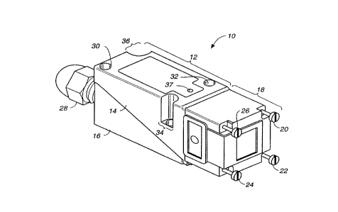
FIGURE 1 is a perspective view of an rf reader having a rotatably
adjustable head mounted to a body portion in accordance with the present
10 invention.
FIGURE 2 is a perspective view of the rf reader of FIGURE 1 with its
rotatably adjustable head portion extracted from its body portion to expose
the liquid-tight O-ring assembly contained therein in accordance with the
16 present invention.
FIGURE 3 is a perspective view of the rf reader of FIGURE 1 with
the upper and lower halves of the body portion separated to expose a gasket
located between the two halves in accordance with the present invention.
FIGURE 4 is a top view of the rf reader of FIGURE 1 with the upper
half and the rotatably adjustable head portion removed therefrom to expose
interior screw termin~l~ located in the bottom half of the body portion in
accordance with the present invention.
FIGURE 5 is a schematic diagram of the antenna circuitry and the
read/write electronics circuitry in accordance with the present invention.
FIGURE 6 is a more detailed s~h~m~tic diagram of the synchronous
30 switching power supply of Figure 5 showing various components of the
synchronous switching power supply in accordance with the present
invention.
FIGURE 7 is a schematic view of multiple rf readers attached via
35 respective interfacing cables to a wire bus in accordance with the present
invention.
CA 022171~8 1997-10-02
W O96131787 PCT~US9G/01032
Best Mode for Carrying Out the Invention
Reference will now be made in detail to the preferred embodiments
of the invention, examples of which are illustrated in the accompanying
drawings. While the invention will be described in conjunction with the
preferred embodiments, it will be understood that they are not intended to
limit the invention to these embodiments. On the contrary, the invention is
intended to cover alternatives, modifications and equivalents, which may
be included within the spirit and scope of the invention as defined by the
10 appended claims.
With reference now to Figures 1, a perspective view of the rf reader
10 of the present invention is shown. As shown in Figure 1, rf reader 10
has a body portion 12 formed of two halves, upper half 14 and lower half 16,
15 and a head portion 18. Body portion 12 contains read/write electronics,
while head portion 18 contains an antenna. Rf reader 10 also contains a
gland nut 28 for providing a liquid-tight seal between an interfacing cable,
not shown, and an opening, not shown, in body portion 12 for receiving the
interfacing cable.
ao
In the present embodiment, head portion 18 is attached to body
portion 12 using screws 20, 22, 24, and 26. Although screws 20, 22, 24, and
26 are used in the present embodiment, the present invention is also well
suited to the use of numerous other types of attachment devices or
25 methods. Head portion 18 is rotatably mounted to body portion 12 in the
present embodiment. That is, when screws 20, 22, 24, and 26 are loosened,
head portion 18 can be rotated in 90 degree increments to focus the antenna
towards a desired direction. After rotatably adjustable head portion 18 has
been placed in the desired position, screws 20, 22, 24, and 26 are tightened
30 to hold rotatably adjustable head portion 18 firmly in its desired fixed
position. In addition to directing the antenna outward, the present
invention is also well suited to transmitting and receiving .~ign~l.c through
the top of rotatably adjustable head portion 18. In so doing, the present
invention further increases the possible areas with respect to body portion
35 12 which can be covered by the antenna. Therefore, the antenna of the
present invention is able to be directed in almost any direction regardless of
the position in which the rf reader is mounted.
CA 022171~8 1997-10-02
W O96/31787 PCTrUS~G,~ 32
Two screws 30 and 32 are used to hold upper half 18 and lower half
20 of rf reader 10 together. By unfastening screws 30 and 32, upper half 18
can be easily detached from lower half 20, thereby providing easy access to
the interior of body portion 12. In the present embodiment, rf reader 10 is
completely liquid-tight. That is, upper and lower halves 14 and 16 have a
liquid-tight seal therebetween. Likewise, rotatably adjustable head portion
18 is sealed in a liquid-tight manner to body portion 12. Thus, rf reader 10
of the present invention is impervious to liquids such as oil, water, cutting
fluids, and the like. Therefore the present invention is well suited to use in
10 harsh climates such as, for example, manufacturing facilities. Rf reader
10 also includes an indicator light 37.
In the present embodiment, indicator light 37 is used to indicate the
activity status and the current configuration parameters of the rf reader
15 unit. Furthermore, rf reader 10 includes attachment holes 34 and 36 for
att~hinE the rf reader 10 to a standard mountings. As a result, the
present invention is well suited to use in conventional manufacturing
facilities having standard mountings built therein.
ao With reference next to Figure 2, a perspective view of rf reader 10 is
shown with rotatably adjustable head portion 18 extracted from body
portion 12 to expose O-ring 40. The antenna within rotatably adjustable
head 18 is connected to body portion 12 via a circular access hole 38. O-ring
40 disposed around access hole 38 is formed of a material which, when
25 compressed by att~chinE rotatably head 18 to body portion 12, prevents
liquid from entering hole 38. A short internal electrical connector 42 is
disposed within access hole 38 to electrically connect antenna circuitry
within rotatably adjustable head 18 to read/write electronics circuitry
within the body portion 12. By using O-ring assembly 40 the liquid-tight
30 seal is maintained regardless of the orientation of rotatably adjustable
head 18 with respect to body portion 12.
Referring now to Figure 3, a perspective view of rf reader 10 is
shown with upper and lower halves 14 and 16 separated to expose gasket
35 44. As with O-ring assembly 40 of Figure 2, gasket 44 is formed of a
material which, when compressed by att~ching upper half 14 to lower half
16, ~.~vellts liquid from p~qqinE between the two halves 14 and 16 and into
the interior of rf reader 10. Therefore, as a result of gland nut 28, gasket
CA 022l7l~8 l997-l0-02
W O96/31787 PCTrU59C/0~3
44, and O-ring assembly 40 of Figure 2, rf reader 10 is completely liquid-
tight.
With reference next to Figure 4, a top view of rf reader 10 is shown
with upper half 14 and rotatably adjustable head portion 18 removed
therefrom to expose interior screw termin~ 46a-46e. As shown in Figure
4, an interfacing cable 48 is routed through liquid-tight gland nut 28 and
into the interior of rf reader body portion 12. Individual wires within
interfacing cable 48 are attached to respective screw termin~ 46a-46e.
Screw termin~l.c 46a-46d are electrically connected to the read/write
electronics of rf reader 10. By using screw terminals, the present
invention elimin~tes the need to solder or use other complicated
attachment methods to form electrical connections between interfacing
cable 48 and the read/write electronics. Thus, the present invention is
"user-friendly" allowing for easy on-site installation and repairs.
Referring now to Figure 5, a schematic diagram 50 of the antenna
circuitry 52 and the read/write electronics circuitry 60 is shown. In the
present embodiment, antenna circuitry 50 is comprised of an antenna coil
54, an antenna driver 56 and an antenna receiver 58. Thus, the rf reader
communicates with an rf tag via rf antenna 54. When transmitting to the
rf tag, antenna driver 56 is employed. Likewise, when receiving response
signals from the rf tag, antenna receiver 58 is used. In the present
embodiment, rf antenna 54 is formed of wire-wrapped ferrite which is
securely "potted" or mounted within rotatably adjustable head assembly 18
of Figure 1.
As shown in Figure 5 reader body circuit 60 is comprised of a
synchronous switching power supply 62, a transmit modulator 64, a
receive demodulator 66, an interface controller 68, input buffers 70, and
output buffers 72. Modulator 64 is electrically coupled to antenna driver 56.
Demodulator 66 is coupled to antenna receiver 58. Thus, in the present
embodiment, in response to data coming into input buffers 70, the interface
controller 68 activates modulator 64 to produce an interrogation signal.
~ 35 The interrogation signal is transferred through antenna driver 56 to
antenna coil 54. The interrogation is then transmitted to the rf tag. When
response ~sign~l~ are received, they are routed through antenna receiver
58, to demodulator 66, to interface controller 68 and out through output
=
CA 022l7l~8 l997-l0-02
WO96/31787 PCTrU~J,'~I-32
buffers 72.
In the present invention, because antenna circuitry 52 and
read/write electronics circuitry 60 are integrated into a single, compact
5 structure, no extended electrical connections are required between
antenna circuitry 52 and read/write electronics circuitry 60. As a result,
the present invention does not suffer from significant power loss or
electrical noise during the transfer of Rign~lg between antenna circuitry 52
and read/write electronics circuitry 60 as found in conventional two-piece
10 rf reader units.
With reference next to Figure 6, a more detailed schematic diagram
of synchronous switching power supply 62 is shown. As shown in Figure
6, synchronous power supply 62 consists of a reverse polarity and over-
1~ voltage protection circuit 74 which protects the read/write electronicscircuitry against incorrect wiring of the voltage input, and protects
read/write electronics 60 from high voltage transients. The input voltage is
passed from reverse polarity and over-voltage protection circuit 74 through
an EMI filter 76 which keeps internally generated voltage spikes from
20 being conducted back out the Voltage In signal wire. A switching power
supply circuit 78 such as, for example, an SGS-Thomson L4972A switching
regulator, cont~ining a drive transistor 80, a pulse width modulator 82,
and a voltage sensor 84, produces a regulated output voltage which is
filtered by filter 86 and which functions as the internal voltage for
25 read/write electronics 60. Specifically, voltage sensor 84 of switching
power supply circuit 78 samples the output voltage, or "internal voltage" to
determine whether the internal voltage is higher or lower than the desired
value. Voltage sensor 84 controls pulse width modulator 82 which, in
turn, varies the duty cycle of the switching pulse. The switching pulse
30 turns on and off a pass through p-n-p transistor 8Q which meters the
amount of energy transferred to filter 86.
In the present embodiment, antenna driver 56 generates an
interrogation signal which is transmitted from rf antenna 54 at a
35 frequency of appr-)~im~tely 134 KHz. Response .cign~l~ from the rf tag are
received at a frequency of approximately 33.5 KHz. Thus, random voltage
spikes or noise generated by a power supply of a conventional rf reader can
obscure or mask response ~ign~ . However, in the present embodiment, a
CA 022171~8 1997-10-02
W O 96/31787 PCTrUS9~/01032
sync signal is supplied to swit~hing power supply circuit 78 by modulator
64 of Figure 5. The sync signal causes any switching transients to occur
coincident with the interrogation frequency. Because the switching
transients occur at a precise frequency as opposed to a randomly varying
6 frequency, the transients can be filtered out by a filter with fixed
components and a fixed notch frequency. Additionally, because the
frequency is synchronous with the transmitting frequency of rf antenna 54
of Figure 1, there are no inter-modulation products. Thus, the present
invention ~limin~tes or substantially reduces random inter-modulation by-
10 products and noise found in conventional rf reader units.
Referring now to Figure 7, a schematic view of multiple rf readers88, 90, and 92 attached via respective interfacing cables 94, 96, and 98 to a
wire bus 100 is shown. Employing a wire bus 100 elimin~tes the need to
16 separately wire each of multiple rf readers 88, 90, and 92 to a central
controller. Instead of having multiple individual connections, wire bus 100
provides a single connection from the central controller to numerous rf
reader units, thereby saving wire, connectors, space, and installation
labor. Thus, the present invention is well suited to use in manufacturing
20 facilities where numerous rf readers may be disposed at various locations.
Instead of having numerous wire connections, a single bus line can
facilitate the numerous rf readers wherever located within the
manufacturing facility. Likewise, instead of having a separate central
controller for each rf reader or for selected groups of rf readers, the present
26 invention allows numerous distantly-located rf readers to be controlled
using a single central controller.
The read/write electronics of the present invention also includes a
built-in menu and non-volatile memory for storing the configuration
30 parameters of the rf reader unit. By having a built-in menu programmed
into, for example, interface controller 68 of Figure 6, the present invention
allows a user at a central controller station to select and implement
desired operating configuration parameters of the rf reader unit. Thus,
the rf reader of the present invention does not require the numerous
36 progr~mming button and switches found on conventional rf readers. As a
result, the size of the present invention can be reduced to an extent not
possible with conventional rf readers. Additionally, by cont~ining non-
volatile memory, the configuration parameters of the rf reader unit
CA 022171~8 1997-10-02
W O96131787 PCT~US9~/01032
remain stored in the read/write electronics even if power is lost.
Thus, the present invention provides an rf reader unit which has
both the antenna-cont~ining head portion and the read/write electronics-
5 cont~ining body portion integrated into a single, compact, structure. Thecompact size of the present invention allows the rf reader to be placed into
cramped locations which are to small for conventional rf reader units.
The present invention is also adapted to fit on standard mountings.
However, the rotatably adjustable head portion of the present invention
10 allows the antenna contained therein to be focused in almost any direction
regardless of the position in which the rf reader is mounted. As a result,
the present invention elimin~tes the requirement for numerous additional
rf reader units to obtain desired antenna coverage. Furthermore, by
having the antenna-cont~ining head portion and the read/write
15 electronics-cont~ininF body portion integrated into a single, compact,
structure, the present invention does not require a cable or other type of
extended electrical connection between the antenna portion and the
read/write electronics portion. Thus, the present invention does not suffer
from power loss or electrical noise due to extended electrical connections
20 between the antenna portion and the read/write electronics portion. By
using a synchronized switching power supply, the present invention does
not generate noise which interferes with response cign~ from the tagged
item. Also, by having a built-in menu and non-volatile memory, the
present invention does not require numerous buttons and switches to
25 program, set, and store operating parameters for the rf reader unit.
The foregoing descriptions of specific embodiments of the present
invention have been presented for the purposes of illustration and
description. They are not intended to be ç~h~ll.ctive or to limit the invention
30 to the precise forms disclosed, and obviously many modifications and
variations are possible in light of the above teaching. The embodiments
were chosen and described in order to best explain the principles of the
invention and its practical application, to thereby enable others skilled in
the art to best utilize the invention and various embodiments with various
35 modifications as are suited to the particular use contemplated. It is
intended that the scope of the invention be defined by the Claims appended
hereto and their equivalents.