Note : Les descriptions sont présentées dans la langue officielle dans laquelle elles ont été soumises.
CA 0222~226 1997-12-19
W097/0260g PCT ~ 6/00380
Photodetector Involving a MOSFET Having a Floating Gate
BACRGROUND
Measurement of weak light levels is a common procedure in
science and technology.
One of the most sensitive photodetectors is photomultiplier
tube (PMT), or just photomultiplier. The basic structure of
this device is a vacuum tube cont~;n;ng a light sensitive
photocathode and an electron multiplier structure. Electric
field by a high voltage is applied over the system. Photons
to be detected hit the photocathode from which they
liberate photoelectrons by a photoemission process. The
electron multiplier consists of a series (typically 6-16)
of secondary emission electrodes, called as dynodes, with
rising electric potential arranged between them. The
photoelectrons from the cathode are directed to the first
dynode where they produce several secondary electrons which
are, in turn, directed to the next dynode where secondary
emission is repeated, and so on. This results in
amplification so that the signal from the output electrode,
anode, is high enough to be handled electronically.
Disadvantages of photomultiplier tubes are relatively high
cost and need for high voltage which limit and complicate
their versatility.
A different class are various semiconductor photodetectors,
e.g. photodiodes, phototransistors. and charge coupled
devices (CCDs). Common to them is that light is allowed to
affect semiconductor material, where it generates charge
carriers (electrons and holes) that are collected to
produce an electrical signal. A problem with semiconductor
detectors is that the carriers have to migrate in the bulk
of semiconductor material where thermal energy produces a
high background noise.
CA 0222~226 1997-12-19
W O 97/02609 PCTn~6/00380
SUk~RY OF THE IN~nENTION
The present invention discloses a new type of photodetector
which is cheap, sensitive and easy to construct. It
comprises an evacuated chamber cont~; n ing a photoemissive
surface capable of liberating electrons (photoelectrons)
through photoelectric effect in response to light photons.
Characteristic to the present invention is that the
photoelectrons are detected by a metal oxide semiconductor
type of field effec:t transistor (MOSFET) having a floating
gate, the gate being suitably charged before measurement.
PhotoeleCtron emission causes a change in gate charge, the
change being indicative to the amount of light received by
the detector.
According to one entbodiment, the photoemissive surface is
unattached to the gate, the latter being charged to a
positive potential before measurement. The positive charge
attracts photoelect:rons and directs them to the gate where
they neutralize its positive charge leading to a decrease
in gate potential, the decrease being indicative to the
amount of light received by the detector.
According to another embodiment, the photoemissive surface
is processed directly on the floating gate which, in this
case, is charged negatively before measurement. The
liberated photoelec:trons are collected to a separate anode
electrode or just to the metal wall of the device casing.
This causes an increase in the gate potential, the increase
being indicative to the amount of light received by the
detector.
During the photoelectron collection phase the presented
photodetector does not require any electric power
(voltage). Obvious]y, however, an additional electric
fields can also be applied, in order to optimize
photoelectron collection.
CA 0222~226 1997-12-19
W O 97/02609 PCT~g6/00380
OPERATION PRINCIPLE OF THE INVENTION
It is characteristic to the invention that electrons
(photoelectrons) liberated from a photoemissive surface by
,l a photoelectric effect in response to light photons are
allowed to affect the surface of the floating gate of a
MOSFET (metal oxide semiconductor type of a field effect
transistor3. The invention is based on measuring the effect
of photoelectrons on the charge stored in the capacitance
of the floating gate of the MOSFET before measurement.
The photoelectrons are collected by mean~ of the effect of
the electric field created by the gate after it has first
been charged to a suitable potential. This initial charging
is accomplished, for example, by applying the FN tunneling
technique.
By measuring the conductivity of the drain-source channel
of the MOSFET, the amount of gate charge can be determined
without destroying the charge itself. This is analogous to
reading out the information stored in an analog EEPROM
memory.
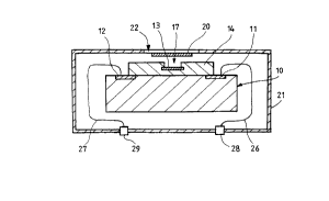
DRAWING
The figure in the drawing shows diagrammatically an
embodiment for the invention.
DESCRIPTION OF THE PREFERRED EMBODIMENT
The figure in the drawing shows diagrammatically one
~T--hoA; ~ent for the photodetector relating to the invention.
It should be noted that the elements of figure are not in
scale. A photoemissive surface 20 receives light photons
and liberates electrons (often called as photoelectrons)
through a photoelectric effect. Photoemi8sive materials are
CA 0222~226 1997-12-19
W 0 97102609 PCTn~6/00380
previously known and can be same as those used in
photocathodes of photomultipliers.
The photoelectrons are detected by the MOSFET 10. This
device has three e]ectrodes: source 11, drain 12 and gate J
5 13. According to the present invention, the gate 13 is ~ept
unconnected, that is, floating. A positive charge is formed
beforehand on the gate 13, for example, by applying a
sufficiently high voltage between the source 11 and the
drain 12. This causes the FN tunneling penomenon to occur
10 through the oxide Layer of the gate insulator 14, causing
the potential in the floating gate 13 to be set at the
desired charge.
It is known that charge-retention properties of MOSFETs
with floating gates are excellent. They are, therefore,
15 well suited for the construction of non-volatile memories,
which include both digital and analog EPROM and EEPROM
memories. Previously, MOSFETs with charged floating gates
have been used as detectors for ionizing radiation, as
shown in PCT Publication WO 95/12134.
20 The positive charge creates an electric field which
attracts photoelectrons and directs them to the gate 13. On
the surface of the gate 13 there is an uncovered area, or
an area covered by conductor, semiconductor or thin
insulator. The thickness of the insulator may not exceed,
25 for example, 1 mm to still enable passage of the electrons
through it to the actual gate. Most preferably, however, a
part of the surface of the gate is completely uncovered.
Accordingly, in the oxide layer insulator 14 of the
floating gate 13 a hole 17 has been formed through which
30 the photoelectrons can directly reach the gate 13 surface.
When hitting the gate 13, photoelectrons neutralize
positive charge thereon, causing a decrease in the gate 13
potential. The amo~mt of potential decrease in a selected
time interval is, t:herefore, indicative to the amount of
35 light received by t;he photodetector in that interval.
CA 0222~226 1997-12-19
W O 97/02609 PCTn~6/00380
For proper operation the photoemissive surface 20 and the
MOSFET 10 are enclosed in a casing 21 which is evacuated to
confine a vacuum. The casing 21 has a transparent portion
22, e.g. of glass, through which light photons can reach
j 5 the photoemissive surface 20. In the figure there is shown
a very useful structure where the photoemissive surface 20
is processed on the interior surface of the transparent
portion 22. The photoemissive surface 20 is connected to
the metal wall of the casing 21. Obviously, the
photoemissive surface can also situate deeper in the
interior cavity of the casing.
The gate 13 potential, being proportional to its charge,
can be determined by measuring the conductivity of the
source-drain channel of the MOSFET 10 without destroying
the charge itself. Conductivity is measured by e.g.
introducing a suitable voltage between source 11 and drain
12 and by measuring the resulting source-drain current. In
other words, the amount of light detected in a selected
time interval can be determined by comparing the source-
drain current after the detection interval to its initialvalue with the gate fully charged.
In order that a charging voltage could be applied between
source 11 and drain 12 and, correspondingly, that the
change in the gate 13 potential (charge) could be measured
as explained above, source 11 and drain 12 are connected by
means of conductors 26 and 27 to connectors 28 and 29,
mounted in the wall of the casing 21.
According to another embodiment of the invention (not
presented in the drawing) the photoemi6sive surface is
processed directly on the gate which, in this case, is
charged negatively before measurement. The liberated
photoelectrons are collected to a separate anode or just to
the metal wall of the casing. This cau6ee an increase in
the gate potential, the increase being indicative to the
amount of light received by the detector. This is
CA 0222~226 1997-12-19
W O 97/02609 P~1/~ /00380
determined by measuring conductivity of the ~ource-drain
channel as above.
It is noteworthy that during the light detection ~i.e.
photoelectron collection) phase, the presented
photodetector does not require any electrical power
(voltage)~ However, it is naturally possible to provide an
additional electric potential between the photoemissive
surface and the floating gate (presented in the figure) or
between the photoemissive surface and the anode (not
presented), in order to enhance and optimize photoelectron
collection.