Note : Les descriptions sont présentées dans la langue officielle dans laquelle elles ont été soumises.
CA 0223~91 1998-04-22
WO 97/21270 PCT~CA96/00271
TI~T. MULTI-Gb/8 DATA R}3CEIV~:R
Field of Invention
his invention relates to a data receiver and more
particularly to a receiver for detecting and amplifying low
level data pulses.
~ckarollnd of the Inventlon
With the current emphasis on the Information
Highway and the explosion of telecommunications in general,
the quantity and speed of data transmission continues to
grow. In the teleco~mtlnications industry, as well as in
computer technology, there exists a neea to transmit large
~uantities of data from point to point, for example between
memory and processors in multiple processor computers. The
large number o~ data bits coupled with the large number of
connections create an interconnect bottle neck which
reguires large numbers of data drivers with their associated
large amount of electrical power. One techni~ue that is
employed to overcome this congestion dif~iculty is to
multiplex large numbers of parallel bit streams up to higher
rate serial bit streams, thus reducing the numbers of
electrical connections that need to be made. The need for
low power multiplex and demultiplex circuits capable of
combining data signals at 50 Mb/s up to 1 Gb/s, ~or example,
has attracted considerable interest among commercial
integrated circuit vendors. Nevertheless, the computer and
communications industries continue to search for lower power
solutions.
Prior ~rt
In addition to the a~orementioned interconnect
bottle neck associated with multi-processor computers, the
high data speeds can also lead to the generation of electro-
magnetic interference (EMI) problems at physical interfacessuch as conventional connectors. One techni~ue that has
been employed success~ully to reduce the number of
SUBSTITUTE SHEET (RULE 26)
CA 0223~91 1998-04-22
WO 97/21270 PCT/CA96/00271
interconnections and EMI in c~mmlln;caticns switching
e~uipment involves a contactless backplane. This techni~ue
is based on directional coupling principles wherein data
transfer occurs between proximate conductors. An example of
one such coupling connector is described in U.S. Patent
5,432,486 which issued July 11, 1995 to Wong and assigned to
Northern Telecom Limited. The technique can be expanded to
permit point-to-multipoint and multipoint-to-point data
transmission over a passive backplane without loss of signal
integrity due to multipoint connectors. In this method,
distribution of the multi gigabit-per-second serial data
employs a form of a.c. coupling, of such small proportions,
that the data information is contained in the data
transitions. Thus a data signal in NRZ format on the
transmission path is coupled to the receiver path as
positive and negative going pulses. The received data at
the demultiplex circuit is considerably attenuated: signal
levels of only 70 mV peak-to-peak, or less, are not
uncommon.
Reliable reception of this data requires special
techniques including signal amplification, wide fre~uency
bandwidth, matched input impedance, and some form of
hysteresis to discriminate against unwanted noise. The
resultant signal must also be capable of being restored to
NRZ format. The present invention relates to the
re~uirement of detecting serial data at gigabit-per-second
rates received over a transmission medium through which the
signal levels have been substantially attenuated.
S~-mm~ry of the Invention
It is an object of the present invention to
provide a data pulse receiver to detect and amplify
attenuated serial data received ~rom a contactless
backplane.
SUBSTITUTE SHEET (RULE 26
CA 0223~i~i91 1998-04-22
WO 97/21270 PCT/CA96/llOZ71
Therefore in accordance with the present invention
there is provided a data pulse receiver. The receiver
comprises a arounded base amplifier having a bipolar
transistor with a base, a collector and an emitter, the base
being connected to a.c.ground. The received data pulses are
provided via an input connected to the emitter through an
impedance matching arrangement. A constant current source
is connected between the emitter and ground. A load
resistor is connected between the collector and a positive
supply. Hysteresis generatina means having its own current
supply is connected in series with the load resistor. An
output terminal to deliver the amplified data output signal
is connected between the collector and the load resistor.
In a preferred embodiment the receiver employs a
pair of grounded base amplifiers, each with its own current
source, in order to accept a differential input.
In a further aspect of the invention, the
hysteresis generating means includes a set-reset flip flop.
Brief DescriDt;on of the Drawinas
The invention will now be described in greater
detail with reference to the attached drawings wherein:
FIGURE 1 is a circuit diagram of a preferred
embodiment of the present invention;
FIGURE 2 is an equivalent circuit for emitter
input impedance;
FIGURE 3 is an e~uivalent circuit for grounded
base amplifier input impedance;
FIGURE 4 shows the variation of 50 ohm termination
impedance as a function of signal level and bias current;
and
FIGURE 5 is a circuit diagram of a data pulse
receiver with automatic hysteresis adjustment.
SUBSTITUTESHEET(RUL~26)
CA 0223~9l l998-04-22
WO 97/21270 PCT/CA96/00271
Detailed DescriDtlon of the Invention
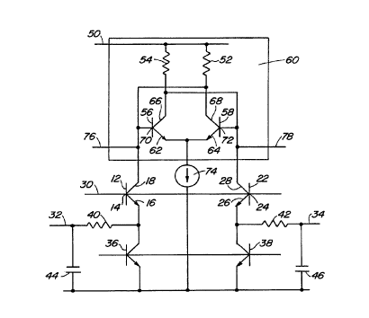
FIGURE 1 is a circuit diagram of one embodiment of
the present invention. The receiver includes grounded base
amplifier 12 having base 14, emitter 16 and collector 18,
and grounded base amplifier 22 having base 24, emitter 26
and collector 28. Bases 14 and 24 are connected to a.c.
ground at 30.
FIGURE 1 is based on a differential input and to
this end the coupled data pulses in differential format are
supplied to negative input 32 and positive input 34. It is
to be understood that the input need not be differential in
which case the receiver would have a single input and a
single grounded base amplifier.
Grounded base amplifiers 12 and 22 have constant
current sources 36 and 38 respectively. Also shown in
FIGURE 1 are input impedance matching resistors 40 and 42.
Capacitors 44 and 46 represent stray capacitance inherent in
the structure.
The collectors 18 and 28 of transistors 12 and 22
respectively are connected to a positive source 50 through
load resistors 52 and 54 respectively. ~oad resistors 52
and 54 in combination with bipolar transistors 56 and 58
form a regenerating flip-flop 60. Regenerating flip-flop 60
reconverts the Return to Zero RZ pulse signal to the
re~uired NRZ format. Transistors 56 and 58 include commonly
connected emitters 62 and 64, collectors 66 and 68, and
bases 70,72. The co~monly connected emitters 62,64 are
provided with tail current by current source 74. Positive
and negative output pulses are provided at terminals 76 and
78 respectively.
The circuit of FIGURE 1 obtains a matching
impedance of, for example, 50 ohms by means of resistors 40
and 42 in the input circuit together with the input
SUBS~lTlrrE SHE~ (P~ULE 26~
CA 0223~91 1998-04-22
WO 97/21270 PCT/CAg6/00271
impedance of the grounded base di~ferential amplifiers 12
and 22. The circuit has the largest possible bandwidth due
to the use of the grounded base transistors. Also ~rom
Kirchoff~s Law, it is clear that, apart from the ef~ect of
parasitic components, the entire signal energy is utilized
~ by the grounded base amplifier. Further, the effect of
parasitic capacitance on the input terminals, which would
normally shunt the input signal, is compensated by the
inductance seen at the emitter of the grounded base
amplifier. This latter effect significantly extends the
fre~uency response of the amplifier. Design of the grounded
base amplifier is as follows:
According to Grey & Meyer, ~Analysis and Design of
Analog Integrated ~ircuits~, Wiley, 3rd Edition 1993, page
497: the input impedance of a grounded base amplifier
~equivalent to that of an emitter follower), has an
equivalent circuit as shown in FIGURE 2. Taking into
consideration the input padding resistance of FIGURE 1, the
grounded base input impedance equivalent circuit is shown in
FIGURE 3. ~earing in mind that this input impedance will
vary depending upon the amplitude of the input signal and
the desirability of attaining an input impedance of
approximately 50 ohms over the full range of the input pulse
amplitude, this dictates the nominal emitter current
required in the grounded base amplifier.
For example:
Suppose the maximum pulse level is 120mV (single
ended~ and the minimllm pulse level is 70 mV.
Then the maximum current pulse expected in a 50
ohm termination is 2.4mA, and according to Kirchoff~s Law,
this current will pass through the grounded base amplifier
~ 35 emitter/collector circuit.
SUBST~TUTE SHEET ~ULE 26)
CA 0223~91 1998-04-22
WO 97/21271~ PCT/CA96/01)271
one can calculate the percentage mismatch error of
the 50 ohm input impedance from:
Error(%) = 100*0.019*((1/(Ie-(Vp/50)))-(1/Ie))/50
where Ie is the emitter bias current and Vp is the pulse
amplitude.
The transistors of the grounded base amplifier
will in general be ~uite large, in order to withstand
electrostatic discharge potentials. Normally this
protection will be augmented by means of parallel diodes
(not shown). As a result, due to the size of the
transistors, the effect of parasitic emitter and base
resistance has been neglected since these will be ~uite
small. The above results have been plotted in FIGURE 4,
showing the variation of impedance mismatch for various
signal levels against the amplifier bias current.
As discussed previously, the grounded base
amplifiers 12,22 are connected to a set-reset flip-flop 60.
The magnitude of the tail current of the flip-flop 60 can be
adjusted by current supply 74 to obtain a controlled amount
of hysteresis. Specifically, the tail current can be
adjusted to whatever threshold current is specified for the
detection of the input signal current. It will be noted
from FIGURE 1 that due to the grounded base amplifiers, the
input signal current passes through the collector load
resistors 52,54 of the flip-flop 60. ALso, the tail current
of the flip-flop 60 passes through the same collector load
resistors. Therefore, to change the state of the RS flip-
flop 60, the voltage produced by the current pulses in thecollector resistors 52,54 must exceed the voltage
established by the tail current of the flip-flop in the same
resistors. The tail current can be easily ad~usted by means
of an external resistor or wired connection, to suit a
particular application. Note that the contribution of the
currents from both amplifier inputs must be taken into
account, assuming the input signal to be differential. If
SUBST!TUTE Sl IEET (i~UL~ 2~)
CA 0223~91 1998-04-22
WO 97/21270 PCT/CA96/00:Z71
the input signal is only applied to one input of the
amplifier, the tail current must be halved for the same
amount of hysteresis. Under normal circumstances the input
~ signal will be differential so as to make the circuit
substantially immune to common mode input noise. It can be
shown from standard communications theory that the required
input noise level relative to the hysteresis level must be
o~ the order of -24ds to obtain a transmission bit error
rate of one error in 10-14.
For example:
For an input pulse hysteresis level of 50mV peak,
a pulse current of 1 mA is transported by both grounded base
amplifier emitter collector circuits, and the bias current
level of the RS flip-flop must be 2mA. To match the input
impedance between 40 to 60 under maximum signal conditions
would re~uire a total power supply current of 5mA (or a
power of 15mW at 3 volt power supply).
Under these last conditions, one can show (from
Grey & Meyer) that a typical input inductance of about 0.5
nH would be obtained for typical medium size (0.8x40 micron
emitters) transistors in a 10 GHz fT bipolar process and
this would help to compensate parasitic capacitances of
several picofarad magnitude at 1 or 2 Gb/s data rates.
FIGURE 5 represents a particular application of
the signal data receiver of the present invention. In this
application the level of the input signal or data at line
102 and 104 is either not known or is variable. Under these
conditions a fixed hysteresis level is undesirable since an
optimum bit error rate cannot generally be obtained. To
overcome this difficulty it is desirable to monitor the
level of the incoming data signal and to adjust the
hysteresis level by automatic means.
SUBSTITUTE SHEET ~RUL~ 26)
CA 0223~91 1998-04-22
WO97/21270 PCT/CA96/00271
A target specification for this data receiver is
that it should be able to detect incoming data pulses with a
peak amplitude of 30 mV and pulse duration exceeding the
hysteresis level of not less than lO~ps. The energy present
in such data pulses is so small that monitoring the level
accurately presents some difficulty. In this regard, recall
that the data pulses are converted ; mm~; ately from RZ
(return to zero) format to NRZ format (non-return to ~ero)
by the pulse receiver circuit. Direct monitoring of the
amplitude of the input data stream has in fact not been
possible. However, an alternative scheme has been employed
which successfully monitors the input pulse height very
accurately and enables optimum adjustment of the hysteresis
level.
The pulse height at the output of the pulse
receiver is primarily determined by the level of the
hysteresis bias current to the set-reset flip-flop of FIGURE
l. Therefore, at the output of the set-reset flip-flop
there is no amplitude information about the incoming data
stream. This flip-flop will togg~e, provided that the input
data signal magnitude exceeds the hysteresis level by an
unknown amount. If the output of the flip-flop is connected
to a differential pair, then the output of the differential
pair will also toggle, if the flip-flop toggles. Further,
common mode variations at the output of the flip-~lop are
not present at the output o~ the differential pair. Thus
the presence or absence of pulses at the output of the
differential pair can be taken to indicate that the
hysteresis level is either less than or greater than the
incoming data pulse magnitude. By a.c. coupling the output
of the differential pair to a rectifier circuit one obtains
a signal whose magnitude is either large, or very small,
depending on whether the hysteresis level is less than or
greater than the incoming data pulse peak magnitude. In
addition, by integrating the output of the rectifier
circuit, a voltage is obtained which can be used to adjust
SUBSTITUTE SHEET ~RUEE 26)
CA 0223~9l l998-04-22
WO97~1270 PCT/CA96/00271
the level of the hysteresis bias current. The net result is
an automatic hysteresis adjustment which continually adjusts
the data pulse receiver hysteresis level to the level of the
data pulses. However, it will be immediately clear that the
adjustment of the hysteresis level to the peak of the data
pulses will result in unreliable reception of the data since
the detector circuit operates as a bang-bang control. As a
result of this, a second data pulse receiver is utilized in
parallel with the one which monitors the data pu~se
magnitude, and the hysteresis level of the second data pulse
receiver is set to a proportionate lower value of that of
the monitoring receiver. It is possible in fact to set the
hysteresis level of the second data pulse receiver to be any
desired proportion of the peak height of the data pulse, a
level of 50% usually results in optimum bit error rate
performance. Of course, when two data ~ulse receivers are
connected in parallel, their individual input impedances are
adjusted to provide a proper combined input termination
impedance.
FIGURE 5 illustrates schematically a data pulse
receiver with automatic hysteresis adjustment. In FIGURE 5,
the data pulses are transferred to the receiver via lines
100,101. The receiver illustrated in FIGURE 1 iS box 102 in
FIGURE 5. The differential pulse input is supplied at input
terminals 104 and 106. The receiver output is taken from
terminals 108 and 110 while the current sink for this
receiver is supplied at terminal 112. Pulse receiver 102 is
used to monitor the data level. Pulse receiver 202 having
input 204,2Q6, outputs 208,210 and hysteresis current 212,
is used to receive the data with very lc-~ bit-error-rate.
It is to be assumed that transistors 116, 118,
172, 174, 176 and 178 are all the same size. P-channel
field effect transistors 166,168 and 170 have different
sizes: in particular the ratio of the transconductance of
transistors 170 and 168 determines the ratio of the current
SUBSTITUTE 5~1EET (RULE 263
CA 0223~9l l998-04-22
W 097/21270 PCT/CA96/00271
sink from receivers 102,202 respectively. Transistor pairs
172,174 and 176,178 are 1:1 mirrors used for monitoring the
current sourced by transistors 170,168 respectively.
Further, if the transconductance of transistor 166 iS less
5 than that of transistor 168 then the P-channel FET mirror of
166,168 Wi ll exhibit current gain. This is of advantage in
increasing the accuracy of the pulse height detector
circuit. In a particular embodiment of the invention,
transistors, 166,168 and 170 have equal channel length and
10 channel widths in the ratio 1:5:10 respectively. In this
arrangement the hysteresis level o~ pulse receiver 202 will
be set to half the data peak amplitude.
The differential output of receiver 102 is
supplied to differential pair 116,118 at bases 120,122,
respectively. Emitters 128,130 are connected to bias
current source 132. Collectors 124,126 are connected to a
positive supply 13 5 via load resistors 134,136 respectively.
The differential pair 116,118 will switch if the output of
pulse receiver 102 switches. This will occur if the data
pulse peak magnitude is greater than the hysteresis level of
the pulse receiver 102. An output of differential pair
116,118 iS taken from load resistor 136 and is a.c. coupled
via capacitor 13 8 to the detector circuit comprising
resistors 140,142 and transistor 150. In a practical
circuit one might also utilize the output from load resistor
134 with an additional parallel connected detector circuit,
thereby increasing the sensitivity of the circuit. The
second detector circuit is not shown in FIGURE 5 for the
sake of simplicity.-
The detection circuit of resistors 140,142 and
transistor 150 is biased by means of a reference voltage at
144 and the ratio of resistors 140 and 142 so that the
voltage at base 152 is just less than a diode voltage drop,
say about 0.75 volts. When pulses are coupled via capacitor
138 to base 152 of transistor 150, they momentarily increase
SUBSTITUTE SHEET (RULE 26)
CA 0223~91 1998-04-22
WO 97/:2~2711 PCT/CA96~0027~
the potential on base 152 and thereby cause transistor 150
to conduct current and so to lower the gate potential o~ FET
166. Capacitor 162 in conjunction with resistor 160 is used
to integrate the pulsed current from transistor 150, so that
transistors 166,168 and 170 conduct a slowly varying
current. The minimum value of the current in these
transistors is set by resistor 164 which therefore sets the
ml ni mllm hysteresis level. This latter feature is useful in
the case of the absence of data, to prevent the ~chattering~
of the data output due to noise pulses. In a particular
example of this circuit in which the data rate was 1.25
Gb/s, the time constant of resistor 160 and capacitor 162
was set to about 20 ns.
It is to be understood that the foregoing
description and drawings attached hereto relate only to
preferred embodiments of the invention. Numerous
alterations or variations may be devised by one skilled in
the art without departing from the spirit and scope of the
invention. The invention is therefore limited only by the
definition thereof in the appended claims.
SUBSTITUTE SHEET (~ULE 26)