Note : Les descriptions sont présentées dans la langue officielle dans laquelle elles ont été soumises.
- CA 0223678~ 1998-o~-o~
W0 97/17763 PCT/SE96~0~395
Universal Receiver Device
Technical Field o~ the Invention
The invention relates to a receiver device for receiving digital
information in the form of electrical differential binary signals
sent from a ~ender device. The receiver device through differen-
tial amplifier circuitry provides the information in a form
suitable to digital logic circuits.
Description of Related Art
Advances in electronic technology and design, and a strive
towards boosted performance in terms of power consumption and
speed, among many other things, has led to a variety of concepts
for digital logic circuits and digital signalling between cir-
cuits and circuit boards. Early concepts are DTL (Diode-Tran-
sistor Logic), TTL (Transistor-Transistor Logic) and ECL (Emitter
Coupled Logic), which concepts are used both within digital logic
circuits and for digital signalling between circuits and circuit
boards.
More recent concepts, mostly used between circuits and circuit
boards, employ differential signalling, also known as balanced
signalling, which uses two signalling wires DPECL (Differential
Pseudo Emitter Coupled Logic), LVDS (Low Voltage Differential
Signalling) and GLVDS (Grounded Low Voltage Differential Signal-
ling) are examples of signalling concepts which use differential
signalling. GLVDS is disclosed in the Swedish patent applications
number SE 9304025-1 and number SE 9400971-9.
Although the above mentioned differential signalling concepts are
indeed differential, each of the two signalling wires operate at
~ fixed nominal voltages that are related to ground. Each wire ope-
rates at two voltage levels, referred to as low voltage level and
high voltage level, respectively.
DPECL typically has a signalling low voltage level of 3 3 V, and
a high level of 4.1 V. LVDS on the other hand has a low level of
CA 0223678~ 1998-o~-o~
W097/177~ PCT~E96/01395
1.0 V, and a high level of 1.4 V, while GLVDS has a low level of
0.1 V and a high level of 0.4 V. The voltages are related to
ground. Signalling voltages hence span from almost 0 V up to more
than 4 V.
A receiver device for receiving differential signals from the
above described types of signalling concepts is often contained
together with digital logic circuits in one integrated circuit,
in order to reduce packaging, to reduce the required size of
circuit-boards and, ultimately, to reduce cost. Preferably, a
single supply-voltage is used for the integrated circuit, which
supply voltage is shared both by the receiver device and by the
digital logic circuits, whereby costly circuit technologies
capable of handling multiple voltages are avoided. New circuit
technologies however operate at very low supply voltages of 3.3
V or less, which enforces operation of the receiver device at
these very low supply voltages.
At low supply voltages, only a small margin, if any, is provided
for circuitry of a receiver device compatible with DPECL, LVDS,
GLVDS and other signalling concepts. At a low supply voltage,
circuitry of such a receiver device must operate at common-mode
voltages both close to the supply voltage, or even above the
supply voltage, and close to ground, preferably even lower than
ground. Common-mode voltage refers to the average voltage, relat-
ed to ground, at the inputs of circuitry known as a differential
amplifier. Said receiver device is a differential amplifier.
Differential amplifiers exist, which are capable of handling
common-mode voltages close to the supply voltage, and close to
ground. These are known as rail-to-rail amplifiers.
- Known rail-to-rail amplifiers however exhibit a bandwidth and a
propagation delay which are dependent on the applied common-mode
voltage. This reduces the usable bandwidth and the ability of the
amplifier to reject common-mode noise at high speeds, and makes
signal skew quite l~nm~n~geable at high speeds.
SUBSTITUTE SHEET (RULE 26~
CA 0223678~ 1998-0~-0~
WO 97/17763 PCT~SE96~0~39~;
Furthermore, known rail-to-rail amplifiers do not handle common-
-mode voltages higher than the supply voltage, or lower than
ground. At a supply voltage of less than approximately 4.5 V,
known rail-to-rail ampli~iers are therefore not compatible with
e.g. DPECL.
It is known in the art that a voltage dividing network is arrang-
ed at the inputs of a differential amplifier, for increasing the
common-mode range. A voltage dividing network however attenuates
the received signal, which makes it a poor solution ~or signals
having low amplitudes. Moreover, process variations increase
asymmetry of the received signal.
In US patent number 5,111,080 is disclosed a signal transmission
circuit in which a signal is converted into two complementary
signals which are output from a signal transmission circuit via
series resistors. The amplitude of each of the complementary
signals is reduced by the series resistors and terminating
resistors provided on a signal receiving side. The signal
receiving side shifts the level of its received input signal. The
levelshifted signals are amplified by a high-input impedance
differential amplifying circuit.
EP patent number 0579314A1 discloses an input buffer circuit. The
input circuit receives a low level signal and a voltage refer-
ence, which are largely free from disturbing signals. The input
buffer circuit comprises reducing means for reducing an offset
voltage.
The Japanese patent number 4,767,979 discloses a switching
circuit device which uses current mirror circuits. A first group
- of current mirror circuits is provided wherein a plurality of
signal currents supplied via input terminals are superimposed
upon mirror currents and signal currents resulting from the
superimposition are derived as new mirror currents. A second
group of current mirrors is provided to which the new mirror
currents are supplied. The output stages of the second group of
CA 0223678~ 1998-o~-o~ -
W097/17763 PCT~E96/01395
current mirror circuits are connected to each other at a common
point which in turn is tied to the output stage of a current
mirror circuit for supplying a mirror current of a predetermined
magnitude. An output terminal is led out of said common point.
Bias voltage for said second group of current mirror circuits is
controlled so that any desired signal current is selected from
said plurality of signal currents.
The Swedish patent application number 9400593-l discloses a
receiver device in which current mirrors are used in the input
stage.
51 -ry of the Invention
An object of the present invention is to provide electronic
circuitry for a universal receiver device which operates at high
speeds within a broad range of common-mode voltages, even slight-
ly lower than ground and higher than the supply voltage.
This object is accomplished by electronic circuitry of the kind
described in the accompanying claims.
According to the invention, higher speeds can be handled by the
receiver device, and the range of signalling voltages which are
received and processed by the receiver device without corruption
of information is extended as compared to prior art, for a given
supply voltage. Common-mode-rejection is improved.
Brief Description of Drawing3
The invention, together with further objects and advantages
thereof, will become clear from the following description by
making reference to the accompanying drawings, in which:
-
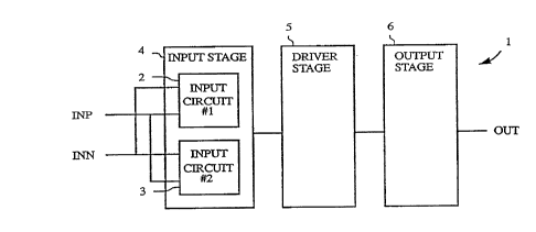
Fig. l is a block diagram of a rail-to-rail amplifier which
constitutes a receiver device on which the invention
is based,
Fig. 2 is a circuit diagram showing a first embodiment of the
receiver device according to fig. l,
- - . CA 0223678~ 1998-0~-0~
WO 97/17763 PCT/SE96~0I395
Fig. 3 is a circuit diagram showing a portion of the embodi-
ment of fig. 2, in which portion certain connections
are highlighted for better illustrating a first input
circuit,
Fig. 4 is a circuit diagram showing a portion of the embodi-
ment of fig. 2, in which portion certain connections
are highlighted for better illustrating a second input
circuit,
Fig. 5 is a circuit diagram showing a second embodiment of
the receiver device according to fig. 1,
Fig. 6 is a circuit diagram showing a third embodiment of the
receiver device according to fig. 1,
Fig. 7 is a circuit diagram showing a ~ourth embodiment o~
the receiver device according to fig. l,
Fig. 8 is a circuit diagram showing a fifth embodiment of the
receiver device according to ~ig. 1.
Detailed Description of the Invention
In fig. 1, a receiver device 1 is shown in the form of a block
diagram. The receiver device 1 has a first input circuit 2, and
a second input circuit 3, which input circuits 2, 3 are connected
in parallel. The input circuits 2, 3 are included in an input
stage 4. Two signal inputs INP, INN are each connected to the two
input circuits 2, 3. The input stage 4 is connected to a driver
stage 5. The driver stage 5 is in turn connected to an output
stage 6. The receiver device 1 receives at its inputs INP, INN
a differential signal, and produces at its output OUT a corre-
sponding signal suitable for digital logic circuits. The receiver
device 1 has a certain common-mode range. The common-mode range
refers to the voltage range of the received signal, related to
a fix reference, e.g. ground, within which the receiver device
- 1 processes said signal without corrupting information being
carried therein. The first input circuit 2 is active within one
portion of said common-mode range, and the second input circuit
3 is active within another portion of said common-mode range.
Said portions may overlap. A receiver device such as this has an
extended common-mode range as compared to receiver devices having
CA 0223678~ 1998-o~-o~ - -
WO97/17763 PCT/SE96/01395
only one input circuit. Allowable common-mode voltages approach
both ground and the supply voltage. Amplifiers possessing this
property are known in the art as rail-to-rail ampli~iers.
Fig. 2 shows a receiver device 7, which is a first embodiment of
the receiver device l according to fig. l. The receiver device
7 comprises N-MOS and P-MOS transistors 8-27, a current generator
28 and an output stage 29. The output stage i8 known per se, and
is therefore not shown in detail. Said transistors 8-27, the
current generator 28 and the output stage 29 are interconnected
as indicated in the drawing.
The current generator 28 feeds a constant current Il through the
channel of the N-MOS transistor 8. The N-MOS transistor 8 is a
part of a circuit arrangement well known in the art as a current
mirror. Said current mirror also comprises the transistors 9-ll.
The transistors 9-ll each sink a constant current I2, I3, I4 which
i8 equal to or proportional to the current Il, provided the
voltage across the channel of respective transistor 9, l0, ll is
sufficiently large, e.g. larger than 0.5 V. The transistors 12,
13 form another current mirror, in which a current I5, sourced by
the transistor 13, is constant and e~ual to or proportional to
the current I2, and therefore also to the current I1, provided
the voltage across the channel of the transistor 13 is suffi-
ciently large. The receiver device 7 comprises further currentmirrors, which will be explained in their respective contexts.
For simplicity, all current mirrors are assumed herein, unless
otherwise noted, to have a one-to-one current-relationship. It
is appreciated by those skilled in the art however, that currents
are scalable in the current mirrors of the receiver device 7.
Actually, power dissipation is decreased in the receiver device
~ 7 by proper scaling of currents. Scaling of currents is also done
to compensate for mismatching propagation delays within the
receiver device.
Two distinct modes of operation, and a combination of the two
modes of operation of the receiver device 7 will be described.
- . CA 0223678~ 1998-0~-0~
WO97/177~ PCT~E96~1395
vcc is set to 3.3 v as an example. In a first distinct mode of
operation, the common-mode voltage, i.e. the average signalling
voltage at the inputs INP, INN iS in the lower region of the
common-mode range o~ the receiver device 7, e.g. around 0.5 V
related to ground. In a second distinct mode of operation, the
common-mode voltage is in the upper region o~ the common-mode
range, e.g. around 2.5 V. In both modes, the voltage at the input
INP minus the voltage at the input INN may be either positive,
negative or zero, i e. either the voltage at the input INP is
lo higher than the voltage at the input INN, the voltage at the
input INN iS higher than the voltage at the input INP, or the
voltages at the inputs INP, INN are equal.
Fig. 3 shows the receiver device 7 in part. Some connections are
highlighted (drawn with thick lines) in order to better illus-
trate a ~irst input circuit corresponding to the first input
circuit 2 of the receiver device shown in fig. 1. The first input
circuit comprises the transistors 13, 14, 15, 16, 17, 18 and 20.
The function in the first distinct mode of operation will now be
described. The transistors 14 and 15 receive form outside the
receiver device the differential signal present at the inputs
INP, INN in the first distinct mode of operation. The differen-
tial signal is received directly at the source terminals o~ the
transistors 14 and 15. The voltage drops UGS Of the transistors
24, 25, 26, 27, are not sufficiently large to make said transis-
tors 24, 25, 26, 27 conduct in the first distinct mode of
operation.
The constant current I5 is drawn through the transistor 15 alone,
through the transistor 14 alone, or through both transistors 14,
15 at the same time, depending on the input signal applied at the
~ inputs INP, INN. Due to a feedback from the drain terminals to
the gate terminals of the transistors 14, 15, the voltage drops
UDS across said transistors 14, 15 can become only slightly
larger than the threshold voltages UGsth of said transistors 14,
15. In effect, if the voltage at the input INP iS considerably
higher than the voltage at the input INN, the voltage drop UDS
CA 0223678~ 1998-o~-o~ - -
W097/17763 PCT/SE96tO1395
across the transistor 15 limits the voltage UG5 across the
transistor 14 such that the threshold voltage UGS~ ~f the
transistor 14 is not reached, and hence the transistor 14 does
not conduct current. The current Is is drawn solely through the
transistor 15. I~, on the other hand, the voltage at the input
INN is considerably higher than the voltage at the input INP, the
voltage drop U~ across the transistor 14 limits the voltage UGS
across the transistor 15 such that the threshold voltage UGsth of
the transistor 15 is not reached, and hence the transistor 15
does not conduct current. The current I5 is drawn solely through
the transistor 14. I~ the voltages at the inputs INP, INN are
approximately equal, both transistors 14, 15 are conducting
current, and each one o~ said transistors 14, 15 draw a respec-
tive portion of the current I
The transistors 14, 16 are comprised in a current mirror, and the
transistors 15, 17 are comprised in another current mirror.
Furthermore, each one of the transistor pairs 18, 19; 20, 21 and
22, 23 is comprised in a respective current mirror. Currents
through the transistors 14, 15 are reflected in respective
currents through the transistors 16, 17. A current through the
transistor 16, and hence also through the transistor 18, is
reflected in a current through the transistors l9, 22. Conse-
quently, the transistor 23 is capable of sinking a current
determined by the current through the transistor 14. Similarly,
a current that is drawn through the transistor 17 is also drawn
through the transistor 20. Consequently, the transistor 21 is
capable of sourcing a current determined by the current through
the transistor 15.
Thus, provided the input voltages at the inputs INP, INN are not
equal, either the transistor 21 sources current to the output
stage, or the transistor 23 sinks current ~rom the output stage.
Accordingly, a resulting voltage at the output stage 29 is either
high, i.e. close to Vc~, or low, i.e. close to GND, determined by
the input signal at the inputs INP, INN. When the voltage at the
input INP iS higher than the voltage at the input INN, e.g. 0.25
- . CA 0223678~ 1998-0~-0~
WO 97/17763 PCT/SE96/01395
v higher, the output OUT iS high and vice versa. Equal voltages
at the inputs INP, INN would cause the voltage being fed to the
output stage 29, and hence being present at the output OUT, to
be indeterminate.
Fig 4 also shows the receiver device 7 in part. Some connections
are highlighted (drawn with thick lines) in order to better
illustrate a second input circuit corresponding to the second
input circuit 3 of the receiver device shown in fig. 1. The
second input circuit comprises the transistors }0, 11, 13, 18,
20, 24, 25, 26 and 27. The function of the receiver device 7 in
the second distinct mode o~ operation will now be described. The
transistors 24, 25 receive form outside the receiver device the
differential signal present at the inputs INP, INN in the second
distinct mode of operation. The differential signal is received
directly at the gate terminals of the transistors 24 and 25.
Moreover, the transistors 26 and 27 receive form outside the
receiver device the differential signal present at the inputs
INP, INN in the second distinct mode of operation. The differen-
tial signal is received directly at the gate terminals of thetransistors 26 and 27, for substantially disengaging the first
input circuit in the second distinct mode of operation.
As previously mentioned, the common-mode voltage in the second
distinct mode of operation is in the upper region of the common
mode range, e.g. around 2.5 V. The transistors 26, 27, shunt the
current I5. NO current is thus drawn through the transistors 14,
15, and consequently the transistors 16, 17 do not conduct
current. Regardless of this, the voltage drop Vcc minus INP or
INN iS not sufficiently large for the transistors 13-17 to
conduct in the second distinct mode o~ operation.
If the voltage at the input INP iS considerably higher than the
voltage at the input INN, the voltage drop UGS across the
transistor 25 is suf~iciently large to make said transistor 25
conduct current, while the voltage drop UGS across the transistor
24 does not reach the threshold voltage UGsth, and hence said
CA 0223678~ 1998-o~-o~ - -
WO97/17763 PCT/SE96/0~395
transistor 24 does not conduct current. The current I4 is drawn
solely through the transistor 25 and through the transistor 20.
Consequently, the transistor 21 is capable of sourcing a current
determined by the current through the transistor 25. If, on the
other hand, the voltage at the input INN is considerably higher
than the voltage at the input INP, the current I4 is drawn solely
through the transistor 24 and through the transistor 18. The
current through the transistor 18 is re~lected in a current
through the transistor 19 and ~urther through the transistor 22.
Consequently, the transistor 23 is capable of sinking a current
determined by the current through the transistor 24. I~ the
voltages at the inputs INP, INN are approximately equal, both
transistors 24, 25 are conducting current, and each one of said
transistors 24, 25 draws a respective portion of the current I4
In the second mode of operation, the current I4 is constant.
When the voltage at the input INP is higher than the voltage at
the input INN, e.g. 0. 25 V higher, the output OUT is hence high
and vice versa. Equal voltages at the inputs INP, INN would cause
the voltage being ~ed to the output stage 29, and hence being
present at the output OUT, to be indeterminate.
Important aspects of the invention are to effect a high usable
bandwidth and a low and essentially constant signal propagation
delay of the receiver device 7 throughout the common-mode range.
Therefore, said ~irst input circuit, and said second input
circuit are mutually matched, as regards bandwidth and propaga-
tion delay. Transistors 14, 15, 24, 25 are used, which are o~ one
and the same type, ~or receiving signals applied at the inputs
INP, INN. Furthermore, the transistors 26 and 27 are the same
type as the transistors 24 and 25, and the transistors 16 and 17
~ are of the same type as the transistors 14 and 15. In this
embodiment, the transistors 14, 15, 16, 17, 24, 25, 26 and 27 are
o~ N-MOS type, because these have higher bandwidth and gain
(transconductance), and a lower propagation delay than do their
complementary P-MOS counterparts. TransiStor gain is o~ particu-
lar importance for transistors in an input circuit of a receiver
CA 0223678~ 1998-o~-o~
WOg7/l7763 PCT/SE96/01395
11
device, which transistors receive signals from outside said
receiver device. Such signals often have a low differential
signal amplitude, that renders compensation of low gain diffi-
cult. A differential signal amplitude is the voltage between the
inputs of a differential amplifier, such as the inputs INP, INN
of said receiver device l.
A constant propagation delay is further accomplished by holding
the sum of the current through the transistor 18 and the current
through the transistor 20 constant across both modes of opera-
tion. If said currents were allowed to vary, the time it would
take for particularly the transistors 21, 23 to respond to
changes would vary, and thus result in a non-constant propagation
delay. The transistors 26, 27 play a significant role in keeping
said currents constant, by controlling activation and deactiva-
tion of the first input circuit Operation between the two
distinct modes of operation will now be described.
For a common-mode voltage around 1.0 V, said first input circuit
is active, and said second input circuit is at the verge of being
active. The current I4 is small. The currents through the
transistors 18, 20 are the aggregate of currents through the
transistors 16, 24 and through the transistors 17, 25. Said
currents equal the sum of the current I4 and the current fed
through the transistors 14, 15. A slight increase in the
common-mode voltage results in a current Iq drawn through the
transistors 18, 20. Due to a similar interconnection of the
transistors 10, 26, 27 and the transistors ll, 24, 25, and good
matching of said transistors 10, 11, 24, 25, 26, 27, the current
I3 drawn through the transistors 26, 27 is equal to the current
I4. The current I3 is drawn from the current I5, whereby the
~ currents through the transistors 14, 15, and hence the currents
through the transistors 16, 17, decrease. The sum of currents
being drawn through the transistors 18, 20 is maintained
constant. At further increases of the common-mode voltage, the
current I4, and consequently the current I3, are successively
increasing until the current-mode is approached, at which point
CA 0223678~ l998-o~-o~
WO97/17763 PCT/SE96/01395
12
said first input circuit is completely deactivated. When the
common-mode voltage is being increased, said second input circuit
is hence gradually becoming more active, while said first input
circuit is gradually becoming more non-active and vice versa.
Thus, the modes of operation are partially overlapping.
Fig. 5 shows a receiver device 28, which is a second embodiment
of the receiver device 1 according to fig. 1. The receiver device
28 has a common-mode voltage range beyond that of the receiver
device 7, shown in fig. 2, at e~ual supply voltages. The allow-
able common-mode voltages exceed the supply voltage. The receiver
device 28 has differential outputs. The receiver device 28 com-
prises N-MOS and P-MOS transistors 29-46, a current generator 47
and resistive elements 48, 49. Said transistors 29-46, the
current generator 47 and the resistive elements are interconnect-
ed as indicated in the drawing.
In the receiver device 28, the resistive elements 48, 49 replace
the transistors 18, 20 of the receiver device 7. If the voltage
at the input INP is higher than the voltage at the input INN,
e.g. 0.25 V higher, a current is drawn through the resistive
element 49, but not through the resistive element 48. The current
through the resistive element 49 results in a voltage drop across
said resistive element 49, which voltage drop lowers the voltage
across the transistor 46, connected as a source follower, such
that the output OUTP is more positive than the output OUTN. If,
on the other hand, the voltage at the input INN is larger than
the voltage at the input INP, the voltage at the output OUTN is
more positive than the output OUTP, which is evident ~rom the
symmetry o~ the circuit.
The receiver device is typically implemented in an integrated
circuit. In a circuit technology that does not provide resistors,
the resistive elements 48, 49 typically consist of transistor
which emulate resistors, in a manner known per se.
Fig. 6 shows a receiver device 50, which is a third embodiment
CA 0223678~ 1998-0~-0
WO 97~17763 PCT/SE96~0139
:L3
of the receiver device 1 according to ~ig. 1. The receiver device
50 comprises N-MOS and P-MOS transistors, a current generator and
voltage generators 55, 56, 57 Said transistors, the current
generator and the voltage generators are interconnected as
indicated in the drawing. Several of the current mirrors of the
receiver device 7 are replaced by current mirrors 51, 52, 53, 54
comprising transistors in cascode arrangements. These cascode
arrangements are essentially known from e g the swèdish patent
application number SE 9400593-1. A reference voltage is however
provided by a voltage generator, e.g. a transistor, not shown,
in the path of the reference current of the current ~irror rather
than by a separate circuit arrangement. Current mirrors compris-
ing cascode arrangements are less voltage dependent than the
simple common types Voltage dependence introduces an error in
the re~lected current o~ a current mirror. A low error is
particularl~ desirable in circuitry comprising several current
mirrors which are chained together, such as in the embodiments
shown herein. An error in the reflected currents multiplies
through the chain of current mirrors, which affects the working
point of a receiver device at variations in the common-mode
voltage and variations in the supply voltage. In a receiver
device implemented in certain circuit technologies, the error
would be quite large if using said simple common types of current
mirrors. This would cause poor operation
Fig. 7 shows a receiver device 58, which is a fourth embodiment
of the receiver device 1 according to fig. 1. The receiver device
58 resembles the receiver device 28, shown in fig. 5, however
transistors 59-66 and connections, which connections are high-
lighted ~drawn with thick lines), have been added according tothe drawing. Shown voltage-generator and current-generator
- arrangements of the transistors 59-66 serve the purpose of
turning voltages applied at the inputs INP, INN into lower
voltages within a second input circuit, said second input circuit
corresponding to the aforementioned input circuit 3 of fig
The receiver device 58 is thereby capable of receiving signals
at its inputs INP, INN at a common-mode voltage much higher than
,
CA 0223678~ 1998-o~-o~ -
WO97/17763 PCT/SE96/01395
the supply voltage Vcc. The common-mode voltage range is hence
further improved compared with the previously described embodi-
ments. At a supply voltage of 3.3 V, the receiver device 7 is
compatible with DPECL, and operates at common-mode voltages
higher than 4.5 V, and lower than -0.5 V.
A propagation delay added by the transistors 63-66 is compensated
for by sinking a larger current through the resistive elements
48, 49 in the second mode of operation than in the first mode of
operation.
Fig. 8 shows a receiver device 67, which is a final embodiment
of the receiver device l according to fig. l. Bipolar transistors
are connected and used as indicated in the drawing. NPN transis-
tors are used rather than PNP transistors because NPN-transistors
exhibit superior bandwidth and gain and less propagation delay
compared with PNP transistors in certain circuit technologies.
In this description, the terms ~speed~ and "bandwidth" refer to
an ability to handle high information transfer rates, i.e. high
frequency signalling. These terms can be regarded herein as
equivalents.
In the accompanying claims, the term ~first transistors~ refers
to the transistors 14 and 15 or corresponding elements 39, 41 or
the like in other embodiments of the invention. The term "second
transistors" refers to the transistors 24 and 25 or corresponding
elements 37, 38 or the like in other embodiments of the inven-
tion. The term "load circuit-elements" refers to the transistors
18 and 20, or to the resistors 48 and 49.
It is obvious for those skilled in the art that the shown embodi-
ments can be almost freely combined into new embodiments without
departing from the scope and the spirit of the invention.
Furthermore, the invention is not restricted to handling of
information in digital form, but may as well be used for analog
,
r ~ , CA 02236785 1998-05-05
WO97/17763 PCT~E96/01395
signals.
For simplicity, the invention has been described using two input
circuits in the input stage 4. The principles of the invention
however also apply to a receiver device comprising three or more
input circuits.