Note : Les descriptions sont présentées dans la langue officielle dans laquelle elles ont été soumises.
CA 02241530 2001-02-19
FIELD OF II~1VENTIOI~I
The present invention relates generally to electrically
conductive devices and, more particularly, to electrically
conductive elastomers and methods for fabricating the same.
BACKGROUND OF THE INVENTION
The evolution of integrated circuits has been to decrease
the package size of an integrated circuit while increasing the
number of electrical leads for electrical interconnection
between the integrated circuit and a circuit board on which it
resides. As the number of e-_ectrical leads per integrated
circuit has inc ceased, the e-~ectrical. iea l,~ :r,:ave become smaller
in size and more closely spaced, thereby increasing the
difficulty in mounting an integrated circuit to a circuit
board.
One method of overcoming this difficulty has been to
replace the electrical leads, which are ~ecated around the
perimeter of an integrated circuit package, with electrical
contacts, which are located on the bottom surface of an
integrated circuit package, thereby forming a leadless
integrated circuit package. These electrical contacts
typvcally have the shape "f small protuberances or "balls"
which are spaced in a grid array pattern. An integrated
circuit package having these bottom surface electrical contacts
is placed within a leadless integrated circuit socket or
mounting device which retains the integrated circuit package.
The mounting device has mating electrical
CA 02241530 1998-06-25
WO 98/18615 PCT/US96/19243
- 2 -
contacts spaced in a grid array pattern which align with the
electrical contacts on the integrated circuit package so as ,
to provide electrical continuity between the integrated
circuit package and a circuit board upon which the mounting ,
device resides.
One problem that arises with leadless integrated circuit
packages is that the electrical contacts of a leadless
integrated circuit package and the mating electrical contacts
of a mounting device become oxidized, which results in
increased contact resistance and therefore decreased
conduction between the electrical contacts of the integrated
circuit package and the mating electrical contacts of the
mounting device. The insertion force used to place a
leadless integrated circuit package into a mounting device
typically removes some of this oxide, thereby providing
improved electrical contact. However, leadless integrated
circuit packages are typically not inserted into a mounting
device in a manner that is conducive to the removal of oxide
on the electrical contacts, and since leadless integrated
circuit packages are not directly soldered to the mounting
device, the accumulation of oxide on the electrical contacts
can result in poor electrical contact.
Another problem that arises with the use of=leadless
integrated circuit packages is that the electrical contacts
of a mounting device are typically electrically connected to
electrical leads which are soldered directly to a circuit
board. The mounting device must therefore be desoldered if
replacement or removal is required. As is commonly known in
the industry, repeated soldering and desoldering typically
degrades the quality of a circuit board, usually to the point
where replacement is required. Thus, a solderless electrical
connection scheme would be desirable.
In the fabrication of electronic or electrical devices
and circuits, conductive paths and contact areas are usually
provided by chemical etching and photolithographic techniques
such as in the fabrication of printed circuit boards, and by
CA 02241530 1998-06-25
WO 98/1.8615 PCT/LTS96l19243
- 3 -
plating techniques whereby one or more metal layers are
provided on, for example, electrical contacts or Contact
areas of circuit boards, electrical devices, and the like.
Such fabrication techniques are well known and are widely
employed. They do, however, require a number of process
steps and specialized fabrication equipment which adds to the
cost and complexity of the manufacturing process and of the
resultant products. Thus, the discovery of simpler
fabrication techniques would be desirable.
SUMMARY OF THE INVENTION
The present invention contemplates several types of
electrically conductive elastoriiers and methods for producing
the same. In one embodiment, the present invention is
realized as a layered composition comprising: a substrate
having an outer surface, wherein the substrate is formed of
a non-conductive elastic material; a first layer that is
grafted to the outer surface of the substrate, wherein the
first layer is formed with a non-conductive elastic material;
and a second layer that is grafted to the outer surface of
the first layer, wherein the second layer is formed with a
non-conductive elastic material having a quantity of
conductive flakes interspersed therein. The second layer can
further be formed with a quantity of rounded or jagged
conductive particles interspersed in the non-conductive
elastic material such that some of the conductive particles
are present along an outer surface of the second layer_
Alternatively, a quantity of rounded or jagged conductive
particles may be imbedded in an outer surface of the second
layer.
' In another embodiment, the present invention is realized
as an elastic conductive interconnect element which has an
' elongated shape and is formed with a non-conductive elastic
material having a quantity of conductive flakes and a
quantity of conductive powder granules interspersed therein.
The elastic conductive interconnect element can further be
CA 02241530 1998-06-25
WO 98/18615 PCT/US96/19243
- 4 -
formed with a quantity of rounded or jagged conductive
particles interspersed in the non-conductive elastic material .
such that some of the conductive particles are present along
an outer surface of said elastic conductive interconnect ,
element.
In still another embodiment, the present invention is
realized as an electrical interconnect comprising a non-
conductive substrate having respective opposite surfaces and
a plurality of apertures formed therein extending between the
respective opposite surfaces; and a corresponding plurality
of elastic conductive interconnect elements located within
the plurality of apertures, wherein each elastic conductive
interconnect element.extends between the respective opposite
surfaces of the substrate, and wherein each elastic
conductive interconnect element is formed-with a non-
conductive elastic material having a quantity of conductive
flakes and a quantity of conductive powder granules
interspersed therein.
The present invention includes the- methods for
fabricating the above-mentioned embodiments, which are
themselves unique due to some novel manufacturing processes.
In view of the foregoing, it is quite apparent how the
present invention overcomes the shortcomings of the above-
mentioned prior art devices.
Accordingly, the primary obj ect of the present invention
is to provide electrically conductive elastomers and methods
for fabricating the same.
The above primary object, as well as other objects,
features, and advantages, of the present invention will
become readily apparent from the following detailed
description which is to be read in conjunction with the
appended drawings.
CA 02241530 1998-06-25
WO 98/18615 PC'1'/US96/I9243
- 5 -
BRIEF DESCRIPTION OF THE DRAWINGS
In order to facilitate a fuller understanding of the
present invention, reference is now made to the appended
drawings. These drawings should not be construed as limiting
the present invention, but are intended to be exemplary only.
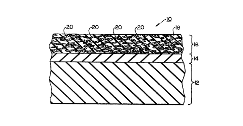
Figure -1 is a cross-sectional view of a layered
composition having an elastic conductive layer according to
the present invention.
Figure 2 is a cross-sectional view of a telephone or
calculator keypad having an elastic conductive layer
according to the present invention.
Figure 3 is a cross-sectional view of a layered
composition having an elastic conductive layer and indenting
particles according to the present invention.
Figure 4 is a cross-sectional view of a layered
composition having an elastic conductive layer and piercing
particle-s according to the present invention.
Figure 5 is a cross-sectional view of a layered
composition having an elastic conductive layer with indenting
particles according to the present invention.
Figure 6 is a cross-sectional view of a layered
composition having an elastic conductive layer with piercing
particles according to the present invention.
Figure 7 is a cross-sectional view of a pushbutton
switch having an elastic conductive layer according to the
present invention.
Figure 8 is a cross-sectional view of an interconnect
device having elastic conductive interconnect elements
according to the present invention.
Figure 9 is a cross-sectional view of. one of the elastic
conductive interconnect elements shown in Figure 8.
Figure 10 is a cross-sectional view of an injection
apparatus for forming elastic conductive interconnect
_elements according to the present invention.
Figure 11 is a cross-sectional view of an elastic
conductive interconnect element having conductive indenting
CA 02241530 1998-06-25
WO 98/18615 PCT/US96/19243
- 6 -
particles according to the present invention.
Figure 12 is a cross-sectional view of an elastic
conductive interconnect element having conductive piercing
particles according to the present invention. ,
DETAILED DESCRIPTION OF THE INVENTION
Referring to Figure 1, there is shown a cross-sectional
view of a layered composition 10 comprising an elastic
substrate 12, an elastic primer layer 14, and an elastic
conductive layer 16. The. elastic substrate 12 may be
fabricated of one of many elastic materials such as, for
- example, silicone rubber or flourosilicone rubber. The
elastic primer layer 14 may also be fabricated of one of many
elastic materials such as, for example, silicone rubber or
flourosilicone rubber. The elastic conductive layer 16
comprises a mixture of an elastic material 18 and a quantity
of conductive flakes 20. The elastic material 18 may further
be fabricated of one of many elastic materials such as, for
example, silicone rubber or flourosilicone rubber_ The
conductive flakes 20 may be fabricated of many different
types of conductive or semiconductive materials such as, for
example,- silver, nickel, or carbon. Alternatively, the
conductive flakes 20 may be fabricated of many different
types of conductive, semiconductive, or insulative materials
which are coated with or have interspersed therein other
conductive or semiconductive materials such as, for example,
silver, nickel, or carbon. The size of the conductive flakes
may vary depending on the level of conductivity that is
required.
The layered composition 10 may be fabricated by a
thermal grafting process which typically begins-by providing
the elastic substrate 12 in a fully cured state . The elastic
primer layer 14 is then deposited on the elastic substrate
12 by spray coating or any other known means. The elastic
conductive layer 16 is then deposited on the elastic primer
layer 14 also by spray coating or any other known means. The
CA 02241530 1998-06-25
WO 98/18615 PCT/US96/19243
entire layered structure is then subj ected to a thermal cycle
E
whereby the elastic primer layer 14 is fully cured and
grafted to the elastic substrate 12, and the elastic
conductive layer 16 is fully cured and grafted to the elastic
primer layer 14. During this thermal grafting process,
polymer chains in the elastic primer layer 14 are grafted to
polymer chains in the elastic substrate 12 so as to form a
strong bond. Likewise, polymer chains in the elastic
conductive layer 16 are grafted to polymer chains in the
elastic primer layer 14 so as to form a strong bond. This
thermal grafting process eliminates the need to etch or
otherwise pretreat the surface of the elastic substrate 12.
There is generally no limitation on the thickness of the
elastic substrate 12. A typical thickness of the combination
of the elastic primer layer 14 and the elastic conductive
layer 16 is in the range of 0.5 to 10 mil. Generally, the
elastic conductive layer 16 is two times as thick as the
'
elastic primer layer 14
. The durometer rating of all of the
elastic materials typically ranges between 40 and 80 on the
Shore A scale. The resistance of an elastic conductive layer
16 having all of the above-stated characteristics has been
shown to be in the range of 20-30 mohm during measurements
performed by compressively mating the surface of the elastic
conductive layer 16 with a Sn/Pb trace on a printed circuit
board.
The conductive flakes 20 which are suspended within the
elastic material 18 of the elastic conductive layer 16
provide low resistivity even when the elastic conductive
layer 16 is being deformed through expansion or compression
since the surface area of the conductive flakes 20 is large
' enough for electrical contact to be made between adjacent
conductive flakes 20 when such deformities occur. For
' instance, during lengthwise expansion of the elastic
conductive layer 16, the length of the elastic conductive
layer 16 is increased while the thickness of the elastic
conductive layer 16 is decreased. The decrease in thickness
CA 02241530 1998-06-25
WO 98/I8615 PCT/US96/19243
. _ g _
brings adjacent conductive flakes 20 closer together, thereby
increasing the likelihood that the large surface areas of ,
adjacent conductive flakes 20 will come into physical, and
hence electrical, contact with each other. The increase in
length results in lateral movement of the conductive flakes
20, thereby causing the large surface areas of adjacent
conductive flakes 20 to rub or scrape against each other so
that physical , and hence electrical , contact between adj acent
conductive flakes 20 is maintained.
One particular application wherein the above-described
layered composition 10 would be useful is a telephone or
calculator keypad wherein an electrical connection must be
made by pressing a key on the keypad. If such a keypad were
constructed with an elastic material such as, far example,
silicone rubber or flourosilicone rubber, an elastic
conductive layer could be grafted onto a surface of that
elastic material according to the process described above.
Thus, when a key of the keypad is pressed against a mating
conductive device, such as a conductive trace on a printed
circuit board, an electrical connection would be made between
the elastic conductive layer and the conductive trace.
Referring to Figure 2, there is shown a cross-sectional
view of a telephone or calculator keypad 100 comprising an
elastic cover 102 having keys 104 formed therein. On the
underside of the cover 102, beneath each of the keys 104, an
elastic primer layer 106 is grafted to the elastic-cover 102
and an elastic conductive layer 108 is grafted to the elastic
primer layer 106_
A printed circuit board 110 is positioned beneath the
entire cover 102, and conductive traces 112 are formed on the
printed circuit board 110 beneath the keys 104. Thus, when
a force F is applied to one of the keys 104 of the elastic
cover 102 from, for example, a human finger 114, the elastic
conductive layer 108 will come into electrical contact with
a corresponding one of the conductive traces 112.
Referring to Figure 3, there is shown a cross-sectional
CA 02241530 1998-06-25
WO 98/18615 PCT/US96/19243
view of a layered composition 30 similar to the layered
composition 10 described in Figure 1, but with conductive
indenting particles 32 imbedded into the surface of the
elastic conductive layer 16. The conductive indenting
particles 32 are applied to the surface of the elastic
conductive layer Z6 prior to the thermal cycle so that the
particles 32 are secured to the elastic conductive layer 16
when it fully cures. The indenting nature of the conductive
indenting particles 32 provides a means by which an
insulating oxide which may have formed on a conductive
surface which is to mate with the elastic conductive layer
16 may be pushed aside so that an improved electrical
connection may be formed between that conductive surface and
the elastic conductive layer 16. Tt should be noted that the
conductive indenting particles 32 may push aside other
contaminants such as fibers and particulates which may be
present on a mating conductive surface.
The conductive indenting particles 32 may be fabricated
of many different types of conductive or semiconductive
materials such as, for example, silver, nickel, or carbon.
Alternatively, the conductive indenting particles 32 may be
fabricated of many different types of conductive,
semiconductive, or insulative materials which are coated with
or have interspersed therein other conductive or
semiconductive materials such as, for example, silver,
nickel, or carbon. The conductive indenting particles 32
typically have a 50 ~.m average particle size.
Referring to Figure 4, there is shown a cross-sectional
view of a layered composition 40 similar to the layered
composition 10 described in Figure 1, but with conductive
' piercing particles 42 imbedded into the surface of the
elastic conductive layer 16. The conductive piercing
' particles 42 are applied to the surface of the elastic
conductive layer 16 prior to the thermal cycle so that the
particles 42 are.secured.to the elastic conductive layer 16
when it fully cures. The piercing nature of the conductive
CA 02241530 1998-06-25
WO 98/I8615 PCT/US96/19243
- 10 -
piercing particles 42 provides a means by which an insulating
oxide which may have formed on a Conductive surface which is
to mate with the elastic conductive layer 16 may be pierced
so that an improved electrical connection may be formed
between that conductive surface and the elastic conductive
layer 16. It should be noted that the conductive piercing
particles 42 may pierce through other contaminants such as
fibers and particulates which may be present on a mating
conductive surface.
Similar to the conductive indenting particles 32, the
conductive piercing particles 42 may be fabricated of many
different types of conductive or semiconductive materials
such as, for example, silver, nickel, or carbon.
Alternatively, the conductive piercing particles 42 may be~
fabricated of many different types of conductive,
semiconductive, or insulative materials which are coated with
or have interspersed therein other conductive or
semiconductive materials such as, for example, silver,
nickel, or carbon. The conductive piercing particles 42
typically have a 40 ~Cm average particle size.
Referring to Figure 5, there is shown a cross-sectional
view of a layered composition 50 similar to the layered
composition 10 described inFigure 1, but with an elastic
conductive layer 52 comprising a mixture of the elastic
material 18, a quantity of the conductive flakes 20, and a
quantity of the conductive indenting particles 32. In the
fabrication of this layered composition 50, the conductive
indenting particles 32 are deposited on the elastic primer
layer 14 along with the elastic material 18 and the
conductive flakes 20. The distribution of the conductive
indenting particles 32 in the elastic conductive layer 52 is
shown to be near the surface of the elastic conductive layer
52 since the conductive indenting particles 32 are more
likely than the conductive flakes 20 to bounce off the
elastic primer layer 14 during the application of the elastic
conductive layer 52. Of course, this location for the
CA 02241530 1998-06-25
WO 98!18615 PCT/CTS96/19243
- ll -
conductive indenting particles 32 is preferable based on
their functionality (e. g., to push aside oxide on a mating
conductive surface). The amount of the conductive indenting
particles 32 in the elastic conductive layer 52 need
typically only be 5o nominal by weight in order to insure
their proper functionality.
Referring to Figure 6, there is-shown a cross-sectional
view of a layered composition &0 similar to the layered
composition 10 described in Figure l, but with an elastic
conductive layer 62 comprising a mixture of the elastic
material 28, a quantity of the conductive flakes 20, and a
quantity of the conductivepiercing particles 42. In the
fabrication of this layered composition 50, the conductive
piercing particles 42 are deposited on the elastic primer
layer 14 along with the elastic material 18 and the
conductive flakes 20. The distribution of the conductive
piercing particles 42 in the elastic conductive layer 62 is
shown to be near the surface of the elastic conductive layer
62 since the conductive piercing particles 42 are more likely
than the conductive flakes 20 to bounce off the elastic
primer layer 14 during the application of the elastic
conductive layer 62. Of course, this location for the
conductive piercing particles 42 is preferable based on their
functionality (e. g., to pierce through oxide on a mating
conductive surface). The amount of the conductive piercing
particles 42 in the elastic conductive layer 62 need
typically only be 5~ nominal by weight in order to insure
their proper functionality.
At this point it should be noted that the elastic
substrate 12 in all of the above-described layered
compositions 10, 30, 40, 50, and 60 may be replaced with a
material that is merely flexiblesuch as, for example, the
- thermal plastics polyimide (known by the trade name captonT"")
or polyamide (known by the trade name nylonT""). The elastic
primer layer 14 would be grafted to such a flexible substrate
in the manner described above, along with the grafting of the
CA 02241530 1998-06-25
WO 98/18615 PCT/US96/19243
- 12 -
elastic conductive layer 16 to the elastic primer layer 14.
One particular application wherein a layered composition
that is similar to one of the above-described layered
compositions 10, 30, 40, 50, and 60, except having a flexible
substrate, would be useful is a pushbutton switch wherein an
electrical connection must be made by pressing a button of
the switch. If the button of such a switch were constructed
with a flexible material such as, for example, polyimide or
polyamide thermal plastic, an elastic conductive layer could
be grafted onto a surface of that elastic material according
to the process described above. Thus, when the button of
such a switch is pressed against a mating conductive device,
such as metal contacts, an electrical connection would be
made between the elastic conductive layer and the metal
contacts.
Referring to Figure 7, there is shown a cross-sectional
view of a pushbutton switch 200 comprising a housing 202 for
containing a recoil spring 204 and a button actuator 206.
The housing 202 provides metal contacts 208 with access to
the interior thereof.
The button actuator 206 is fabricated of a flexible
thermal plastic material such as, for example, polyimide or
polyamide. An elastic primer layer 210 is grafted to a
bottom contact surface of the button actuator 206, and an
elastic conductive layer 212 is grafted to the elastic primer
layer 210. When a force F is applied to the button actuator
206, the elastic Conductive layer 212 will come into
electrical contact with the metal contacts 208, thereby
closing the switch 200.
At this point it should be noted that any of the above-
described layered compositions 10, 30, 40, 50, and 60 may be
utilized with the telephone or calculator keypad 100 of
Figure 2 or the pushbutton switch 200 of Figure 7, or with
-any number of other devices wherein the use of an elastic
conductive layer~would be useful.
It should also be noted that the elastic conductive
CA 02241530 1998-06-25
WO 98/18615 PCT/US96/I9243
- 13 -
layers 16, 52, 62, 108, and 212 employed in all of the above-
described layered compositions 10, 30, 40, 50, and 60 are
useful for providing shielding from electric and magnetic
fields, or for providing a conductive plane for grounding
purposes or the like. More particularly, the density and
grouping ofthe conductive flakes 20in the above-described
elastic conductive layers 16, 52, 62, 108, and 212 are such
that extremely effective shielding or grounding layers may
be provided. The above-described elastic conductive layers
16, 52, 62, 108, and 212 may also be used to form electrical
connections with conductive traces on printed circuit boards
simply by forcing the elastic conductive layers 16, 52, 62,
108, and 212 against the conductive. traces.
Referring to Figure 8, there is shown a cross-sectional
view of an interconnect device 70 comprising an insulating
substrate 72 having an array of openings 78 formed therein.
An elastic conductive interconnect element 74 is situated
within each opening 78: Such an interconnect device 70 may
be used, for example, to provide electrical connections
between electrical contacts on a leadless integrated circuit
package and electrical contacts on a printed circuit board.
Such electrical contacts may be of the ball or the land grid
array variety.
Referring to Figure 9, there is shown a cross-sectional
view of one of the elastic conductive interconnect elements
74. The elastic conductive interconnect element 74 comprises
a mixture of the elastic material 18, a quantity of the
conductive flakes 20, and a quantity of conductive powder
granules 76. The conductive powder granules 76 may be
fabricated of many different types of conductive or
semiconductive materials such as, for example, silver,
nickel, or carbon. The size of the conductive powder
' granules 76 may vary depending on the level of conductivity
that is required.
The conductive powder granules 76 provide conductive
bridges between the conductive flakes 20, thereby increasing
CA 02241530 1998-06-25
WO 98/18615 PCT/CTS96/I9243
- 14 -
the conductivity of the elastic conductive interconnect
element 74. The amount of the conductive powder granules76 .
that must be added to the mixture of the elastic material 18
and the conductive flakes 20 to provide such an increase in
conductivity may vary depending on the level of conductivity
that is required.
Referring to Figure 10, there is shown a cross-sectional
view of an inj ection apparatus 80 for forming the elastic
conductive interconnect elements 74 in the openings 78 of the
insulating substrate 72. The apparatus 80 comprises an upper
mold section 82 having injection vias 84 formed therein, and
a lower mold section 86. The mixture of the elastic material
18, the conductive flakes 20, and the conductive powder
granules 76 flows down through the vias 84 and fills the
empty voids formed between the upper 82 and lower 86 mold
sections and the openings 78 in the insulating substrate 72.
The mixture is initially heated, but it is later cooled so
as to allow it to cure. The cooling results in an expansion
of the mixture so that the elastic conductive interconnect
elements 74 are securely positioned in the openings 78. It
should be noted that the shape of the upper 82 and lower 86
mold sections in the areas of the interconnect elements may
vary according to the particular application of the
interconnect elements (e. g., interconnecting land grid array
contacts or interconnecting ball gird array contacts).
Referring to Figure 11, there is shown a cross-sectional
view of an elastic conductive interconnect element 90 similar
to the elastic conductive interconnect element 74 shown in
Figure 9, but with a quantity of the conductive indenting
particles 32 added to the mixture of the elastic material 18,
the conductive flakes 20, and the conductive powder granules
76. Similar to the elastic conductive layer 52 described
above in Figure 5, the amount of the conductive indentiz~.g
particles 32 in the elastic conductive interconnect element
90 need typically~only be 5~ nominal by weight in order to
insure their proper functionality. It should be noted that
CA 02241530 1998-06-25
WO 98/18615 PCT/US96/19243
- 15 -
the conductive indenting particles 32 may instead be added
to just the surface of an elastic conductive interconnect
element after the element has been formed but before it fully
cures.
Referring to Figure 12, there is shown a cross-sectional
view of an elastic conductive interconnect element 110
similar to the elastic conductive interconnect element 74
shown in Figure 9, but with a quantity of the conductive
piercing particles 42 added to the mixture of the elastic
material-18, the conductive flakes 20, and the conductive
powder granules 76. Similar to the elastic conductive layer
62 described above in Figure 6, the amount of the conductive
piercing particles 42 in the elastic conductive interconnect
element 90 need typically only be 5~ nominal by weight in
order to insure their proper functionality. It should be
noted that the conductive piercing particles 42 may instead
be added to just the surface of an elastic conductive
interconnect element after the element has been formed but
before it fully cures.
The present invention is not to be limited in scope by
the specific embodiments described herein. Indeed, various
modifications of the present invention, in addition to those
described herein, will be apparent to those of skill in the
art from the foregoing description and accompanying drawings
.
Thus, such modifications are intended to fall within the
scope of the appended claims.