Note : Les descriptions sont présentées dans la langue officielle dans laquelle elles ont été soumises.
CA 02241779 1998-06-26
INDIRECT X-RAY IMAGE DETECTOR FOR RADIOLOGY
BACKGROUND OF THE INVENTION
Field of the Invention
This invention relates to an indirect x-ray image
detector suitable for radiology. The term "indirect"
means that the x-rays are not directly converted into
electrical charges, but rather they are first converted
into light using a scintillator, and then light is
converted into electrical charges by appropriate means.
More particularly, this invention relates to an x-ray
detector where the usual array of pixelated photodiodes
used to convert light into electrical charges, is
replaced by a photoreceptor formed of a thin uniform
layer of photosensitive selenium having a multilayer
structure.
Description of the Prior Art
It is well known to produce indirect x-ray image
detectors based on a system comprising a thin film
transistor (TFT) matrix deposited on a glass substrate
and a corresponding array of photodiodes with an inherent
capacitor, as well as an electrode connected to the
source of the TFT. The photodiodes are covered with a
common transparent electrode and a scintillator. Scanning
circuits are connected to the lines of the TFT array
while reading circuits are connected to the columns of
the TFT matrix.
In such known devices, initially, all the free
electrodes of the photodiodes are biased at the same
-1-
CA 02241779 1998-06-26
reference voltage. The detector undergoes an exposure.
Light is generated in the scintillator which causes the
photodiodes to generate and leak charges. The associated
capacitance of each photodiode releases a charge
proportional to the local exposure resulting in a charge
topography over the entire detector. The scanning
circuits scan the lines in sequence switching the TFTs
and successively connecting the free electrode of each
photodiode-capacitance on the active line to the virtual
reference voltage of the columns. These columns are
connected to a read-out preamplifier which integrates the
charge required to bring back the photodiodes to the
reference potential. During the time of a line
connection, the readout circuit on each line processes
the integrated charges and multiplexes them to an output
buffer memory where the entire two dimensional image
builds up. In these arrangements, the TFTs can also be
replaced by switching diodes. Such TFTs or switching
diodes and photodiodes are generally made of amorphous
silicon. TFTs can also be made of CdSe material. The
scintillator is generally made of evaporated CsI.
One such prior art arrangement using a scintillator
detector crystal, preferably made of a thallium doped
cesium iodide crystal, and an array of photodiodes
arranged to receive the scintillator photons, is
disclosed in U.S. Patent No. 5,171,998 of Engdahl et al.,
for gamma ray imaging.
Another prior art arrangement is disclosed in U.S.
-2-
CA 02241779 2003-03-26
Patent No. 5,198,673 of Rougeot et al. where a
scintillator is optically coupled to a large area
photosensor which is disposed on a substrate and is
electrically coupled to a data read and reset circuit.
The large area photosensor is provided with an amorphous
selenium photosensitive material that exhibits avalanche
multiplication gain when a selected high biasing voltage
is applied, but which does not have a multilayer
structure and requires a biasing voltage between lOOV and
1000V to cause the photosensor to exhibit avalanche
multiplication. In this patent, there is also included a
protective TFT coupled to the data read and reset circuit
to provide overvoltage protection from the high biasing
voltage.
A further prior art detector is disclosed in U.S.
Patent No. 4,363,969 of Ong where an array of optically
isolated small area scintillators overlay a
duophotoconductive sandwich structure that includes a
photoconductive layer which acts as a switch. Both
photoconductive layers can be made of amorphous selenium.
This system uses a duo-dielectric sandwich structure, but
does not use an active matrix substrate such as a TFT.
Also, the construction of an array of scintillators is a
complex and difficult task which has not achieved
widespread application.
A still further prior art x-ray detector is
disclosed in U.S. Patent No. 5,464,984 of Cox et al. It
includes a scintillator, a sensor array of silicon-on-
-3-
CA 02241779 2008-12-12
insulator substrate (SOI), processing circuits and a
ceramic layer which overlays the processing circuits. No
photosensitive selenium is, however, used in this patent.
Also, U.S. patent No. 5,585,638 of Hoffman discloses
an x-ray detector assembly that comprises an imaging
device formed by a scintillator in front of a two-
dimensional photodetector array. The active layers are
formed on a surface of substrate and a uniform first
electrode layer is applied over the entire major surface
on one side of the substrate and serves as a high voltage
bias electrode. Then, a thin semiconductive layer which
constitutes a second electrode, extends over the first
electrode layer and provides an electrical characteristic
that varies in response to impingement of x-rays. Again,
no photosensitive selenium is used therein.
Such prior art devices present a number of
disadvantages in terms of high cost and poor resolution.
Also, they may be operated only by application of either
high voltage or low voltage, thereby restricting their
field of use.
SUMMARY OF THE INVENTION
In accordance with an aspect of the present invention, there is provided an
indirect x-ray image detector suitable for radiology, comprising:
- an active matrix substrate with scanning and read-out circuits;
-4-
CA 02241779 2008-12-12
,, .
- a photoreceptor deposited over said active matrix substrate and coplanar
thereto, said photoreceptor being made of an amorphous selenium based
multilayer structure having a thickness of between 2 and 50 pm, the
amorphous selenium based multilayer structure being of n-i-p type, wherein
the n-layer is a hole blocking layer and is less than 1 pm in thickness, the p-
layer is an electron blocking layer and the i-layer sandwiched between the n
and p layers is an amorphous selenium layer doped with chlorine and
arsenic, the p-layer being adjacent to the active matrix;
- a light-transparent biaising electrode covering said photoreceptor;
- an x-ray conversion scintillator provided on top of the biaising electrode
and
emitting in the blue spectrum; and
- means for biaising the detector to apply an electric field strength of
between 5 and 50 V/pm across the selenium based multilayer structure
selected so as to operate the structure with no avalanche multiplication.
Preferred embodiments of the present invention provide an
indirect x-ray image detector comprising an active matrix
made, for instance, of TFT arrays or switching diodes,
with scanning and read out circuits, and wherein, over
said active matrix there is deposited a photoreceptor
made of a thin co-planar layer (2-50 m) of amorphous
selenium based multilayer structure, said photoreceptor
being covered with a light transparent biasing electrode
on top of which there is provided an x-ray conversion
scintillator. The indices of refraction of the
scintillator and of the selenium multilayer may be
suitably matched, making use of the light transparent
biasing electrode.
-5-
CA 02241779 2008-12-12
It may be preferable to enclose the selenium photosensitive multilayer
photoreceptor and the scintillator within a suitable housing providing
environmental, electrical and mechanical protection.
In accordance with a preferred embodiment of this
invention, the active matrix is a two-dimensional array
of thin film transistors (TFTs) made, for example, of
-5a-
CA 02241779 1998-06-26
amorphous silicon. Each TFT is normally associated with a
storage capacitance which is usually part of the TFT
architecture. Such active matrix is covered with a
photoreceptor made of a photosensitive n-i-p or p-i-n
multilayer structure comprising: (1) a thin (< 1gm)
selenium hole blocking n-layer doped with a material such
as an alkaline metal (e.g. lithium, sodium, potassium or
cesium) or an oxide or halogenide of such metal; (2) an
amorphous selenium i-layer doped with chlorine and
arsenic and (3) a final thin (< lgm) electron blocking
p-layer of arsenic enriched amorphous selenium. On top of
this multilayer structure there is placed a transparent
co-planar biasing electrode, which may consist of indium
tin oxide (ITO).
The i-layer of amorhphous selenium doped with
chlorine and arsenic may contain 1-100 ppm of chlorine
and 0.1-5% by wt. of arsenic and the p-layer of arsenic
enriched a-Se may contain 1-38% by wt. of arsenic. It
should be pointed out that within the scope of the
present invention, the hole blocking n-layer and the
electron blocking p-layer may be made of any suitable
material producing the desired hole blocking and electron
blocking effect, however, the middle i-layer must be made
of amorhpous selenium doped with chlorine and arsenic.
In the "n-i-p" structure the hole blocking n-layer
is adjacent to the scintillator and the electron blocking
p-layer is adjacent to the active matrix, whereas in the
"p-i-n" structure the reverse is true, namely the n-layer
-6-
CA 02241779 1998-06-26
is adjacent to the active matrix, while the p-layer is
adjacent to the scintillator.
In the p-i-n arrangement, the selenium structure
comprises an "n" hole blocking layer deposited on the
active surface of the TFT matrix, thus making contact
with conduction pads on said matrix. On the scintillator
side, an electron blocking "p" layer is provided which is
transparent to the light generated by the scintillator.
An amorphous selenium "i" layer is sandwiched in between
the "n" and the "p" layers. The top electrode is
maintained herein at a negative potential with respect to
the pads periodically connected to the near ground
potential of the drain electrode of the TFTs. Such a
structure need not be protected against high voltage
discharge since the TFTs will become conducting should
the pad voltage reach the negative bias of the TFT gate.
In the alternate n-i-p structure, the biasing
electrode is at a positive potential. Here, a protective
device should be inserted between the pad and the biasing
electrode to avoid the pad potential to grow positively
beyond an allowable voltage and destroy the TFT. This
could happen, for instance, under severe overexposure.
The voltage protection device could be made of an
amorphous silicon TFT shunting the storage capacitance.
A storage capacitance is normally associated with
each TFT switch, however if the selenium layer is thin
enough to provide a proper charge storage, the storage
capacitance will then be an integral part of such
-7-
CA 02241779 1998-06-26
photoreceptor.
The scintillator is preferably made of a blue light
emission material such as cesium iodide doped with sodium
(0.1 - 5% by wt.), rather than thallium, in order to
produce, under the x-ray irradiation, a color glow
matching the maximum photosensitivity of the selenium.
The scintillator layer may also be made of materials such
as calcium tungstate, barium fluoride or sodium iodide,
emitting light in the blue spectrum.
According to this invention, the role of the
selenium multilayer is two-fold. Firstly, it acts as the
light absorber layer thereby converting the incident
energy into electrical charges proportional to the
intensity level of the incident radiation. Secondly, it
acts as the charge transport layer whereby the generated
carriers are transported under the effect of an applied
electric field to the underlying pixelated electrode. The
thickness of the selenium multilayer is much less than
the width of a pixel electrode so that in association
with the direction of the electric field and the high
intrinsic resistance of selenium, the lateral spread of
charge is minimized.
The selenium based multilayer is preferably
optimized for electrical transport where the dark current
is below 200 pA/cm2, preferably below 100 pA/cm2 and the
residual image is less than 5%, preferably less than 1%.
This is achieved by proper control of the compositions
and thicknesses of the individual layers of the
-8-
CA 02241779 1998-06-26
photoreceptor.
Moreover, according to the present invention, the
scintillator layer is preferably deposited directly onto
a combined monolithic structure consisting of the biasing
electrode, the co-planar selenium based multilayer
photoreceptor and the active TFT matrix.
The selenium multilayer is operated under an
electric field (5 to 50 V/ m) having a gain of close to
1, with no avalanche multiplication. This allows the
detector to operate under very high dose rates without
having to saturate the output amplifiers.
BRIEF DESCRIPTION OF THE DRAWINGS
A non-limitative embodiment of the present invention
will now be described with reference to the appended
drawings, in which:
Fig. 1 is a perspective diagrammatical view of a
structure of a detector in accordance with this
invention;
Fig. 2 is a diagrammatic side view of a n-i-p
photoreceptor layer on TFT matrix, with a high voltage
protection device; and
Fig. 3 is a diagrammatic side view of a p-i-n
photoreceptor layer on TFT matrix, which requires no high
voltage protection;
Fig. 4 is a diagrammatic view of a combination of
the scintillator and a-Se photoreceptor with graphs
showing the scintillator emitted light signal wavelength
curve and the selenium photoresponse wavelength curve.
-9-
CA 02241779 1998-06-26
DETAILED DESCRIPTION OF THE INVENTION
In the Figures, the same elements are identified by
the same reference numbers.
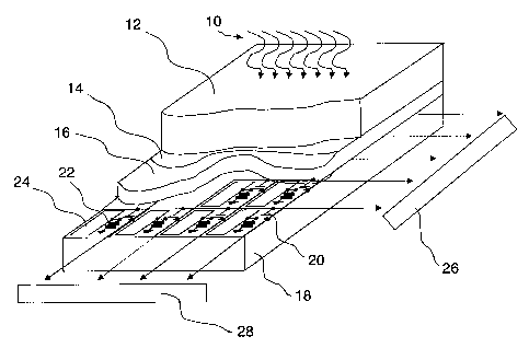
Fig. 1 illustrates an embodiment of the present
invention wherein an x-ray beam 10 is directed onto the
x-ray conversion scintillator 12 which, for example, may
be made of CsI. Such scintillator is typically 300-500 gm
thick and it absorbs about 80% -90% of incoming radiation
while converting x-rays into light. Under the
scintillator 12, there is provided a light transparent
top biasing electrode 14 which can be made of materials
such as ITO. Under this biasing electrode 14, the present
invention provides a co-planar thin (e.g. 5-20 gm) layer
of photosensitive selenium based photoreceptor 16 having
a multilayer structure which converts light into
electrical charges. This photosensitive layer 16 is
deposited onto an active matrix substrate 18 comprising
arrays of TFT switches 20, storage capacitors 22 and
conduction pads 24. Such TFTs may also be replaced by
switching diodes (not shown).
The substrate 18 is also provided, as is known in
the art, with line by line scanning circuits 26 and read
out circuits 28.
It is preferable to enclose the scintillator 12 and
the selenium photosensitive multilayer photoreceptor 16
as well as the biasing electrode 14, within a suitable
housing (not shown) to provide environmental, electrical
and mechanical protection therefor.
-10-
CA 02241779 1998-06-26
Fig. 2 illustrates a n-i-p structure where the
common electrode 14 is under positive bias. Here, on top
of the TFT array 18 and the metal or ITO pads 24,
electron blocking layer 16p made of selenium doped with
arsenic and having a thickness of a few nanometers is
deposited; then is provided layer 16i of several tens of
microns of selenium doped with chlorine and arsenic, and
finally hole blocking layer 16n having a thickness of a
few nanometers, is deposited just under the electrode 14.
Such n-i-p structure is provided with a protective high
voltage device 29 which is inserted between the pad 24
and the biasing electrode 14 to avoid the pad potential
to grow beyond an allowable voltage and destroy the TFTs.
This could happen, for instance, in the event of severe
overexposure.
Fig. 3 illustrates a p-i-n arrangement of the
selenium multilayer photoreceptor 16 on top of which
there is provided the light-transparent biasing electrode
14 which is biased to a negative potential. Here the thin
hole blocking layer 16n is deposited on conduction pads
24 of the active matrix substrate 18 of TFT arrays
comprising TFT switch elements 20 and storage capacitors
22. The thin electron blocking layer 16p is located on
the side of the biasing electrode 14 and is transparent
to the light generated by the scintillator 12. These "n"
and "p" layers are typically a few nanometers in
thickness.
-11-
CA 02241779 1998-06-26
The "i" layer 16i of this p-i-n structure, which is
sandwiched between the "n" and "p" layers is a thin
amorphous selenium layer doped with arsenic and chlorine.
The "i" layer is typically 10 to 20 Acm thick. This
selenium multilayer structure 16 acts as a light absorber
thereby converting the incident light into electrical
charges proportional to the intensity level of the
incident radiation and secondly it acts as a charge
transport layer whereby the generated electrical charges
are transported under the effect of the applied electric
field to the underlying pixelated electrode 18. The top
electrode 14 is herein at a negative potential with
respect to the pads 24 periodically connected to the near
ground potential on the drain electrode of the TFTs. Such
a structure need not be protected against high voltage
discharge since the TFT 18 will become conducting should
the pad 24 voltage reach the negative bias of the TFT
gate.
Fig. 4 illustrates the method of x-ray detection
with a p-i-n detector structure shown in Fig. 3. As shown
in this Fig. 4, the x-ray beam 10 is directed to and
passes through scintillator 12 which may be made, for
example, of a thick layer of cesium iodide doped with
sodium, and where about 80% of incoming x-ray irradiation
is absorbed, and by which the x-rays are converted into
light. The light signal 30 emitted by the scintillator 12
is then passed through transparent top electrode 14 and
the co-planar selenium multilayer 16 which, in this case,
-12-
CA 02241779 1998-06-26
has a p-i-n structure. The top graph shown in Fig. 4
indicates that the peak of the light signal emitted by
the scintillator is at a wavelength of 420 nm. In this
case, the wavelength of the emitted light coming from the
scintillator 12 is made to match the maximum
photoresponse of the selenium multilayer 16.
The selenium multilayer 16 is deposited on
conduction pads 24 of TFT matrix provided with TFT
switching elements 20 and storage capacitors 22. Such TFT
matrix may, if desired, be replaced by switching diodes.
In the case of the set-up shown in Fig. 4, in
operation the top electrode 14 is placed under negative
potential with respect to the pads 24 which are connected
to the ground through capacitors 22. In this manner, no
protection against high voltage discharge is needed since
the TFT will become conducting should the pad voltage
reach the negative bias of the TFT gate.
The selenium photoresponse produced by the
multilayer 16, as shown in the bottom graph in Fig. 4, is
matched to the wavelength peak at 420 nm, emitted by the
scintillator. As a result, the output photocurrent, which
is directly proportional to the emitted light signal, is
optimized.
If instead of a p-i-n structure, a n-i-p structure
of the selenium multilayer 16 is used, then a high
voltage protective device would be required within the
TFT matrix as shown in Fig. 2.
-13-
CA 02241779 1998-06-26
It should be noted that the invention is not limited
to the specific embodiments described above, but that
various obvious modifications can be made by those
skilled in the art without departing from the invention
and the scope of the following claims.
-14-