Sélection de la langue

Search

Sommaire du brevet 2242670 

Énoncé de désistement de responsabilité concernant l'information provenant de tiers

Une partie des informations de ce site Web a été fournie par des sources externes. Le gouvernement du Canada n'assume aucune responsabilité concernant la précision, l'actualité ou la fiabilité des informations fournies par les sources externes. Les utilisateurs qui désirent employer cette information devraient consulter directement la source des informations. Le contenu fourni par les sources externes n'est pas assujetti aux exigences sur les langues officielles, la protection des renseignements personnels et l'accessibilité.

Disponibilité de l'Abrégé et des Revendications

L'apparition de différences dans le texte et l'image des Revendications et de l'Abrégé dépend du moment auquel le document est publié. Les textes des Revendications et de l'Abrégé sont affichés :

  • lorsque la demande peut être examinée par le public;
  • lorsque le brevet est émis (délivrance).
(12) Demande de brevet: (11) CA 2242670
(54) Titre français: LASER A CAVITE VERTICALE ET A EMISSION PAR LA SURFACE A MODULATION PAR CHAMP AVEC UN POMPAGE OPTIQUE INTERNE
(54) Titre anglais: FIELD MODULATED VERTICAL CAVITY SURFACE-EMITTING LASER WITH INTERNAL OPTICAL PUMPING
Statut: Morte
Données bibliographiques
(51) Classification internationale des brevets (CIB):
  • H01S 5/183 (2006.01)
  • H01S 5/04 (2006.01)
  • H01S 3/0941 (2006.01)
  • H01S 5/026 (2006.01)
  • H01S 5/06 (2006.01)
  • H01S 5/34 (2006.01)
  • H01S 5/343 (2006.01)
(72) Inventeurs :
  • WIDMAN, MICHAEL (Suède)
  • KULLANDER-SJOBERG, ANNA (Suède)
(73) Titulaires :
  • MITEL SEMICONDUCTOR AB (Non disponible)
(71) Demandeurs :
  • MITEL SEMICONDUCTOR AB (Suède)
(74) Agent: MARKS & CLERK
(74) Co-agent:
(45) Délivré:
(22) Date de dépôt: 1998-07-09
(41) Mise à la disponibilité du public: 1999-01-14
Requête d'examen: 1998-11-04
Licence disponible: S.O.
(25) Langue des documents déposés: Anglais

Traité de coopération en matière de brevets (PCT): Non

(30) Données de priorité de la demande:
Numéro de la demande Pays / territoire Date
9714820.9 Royaume-Uni 1997-07-14
9718082.2 Royaume-Uni 1997-08-27

Abrégés

Abrégé français

Diode laser à cavité verticale et à émission par la surface (VCSEL), comprenant des miroirs supérieur et inférieur non conducteurs définissant une première cavité contenant un matériau actif et conçue pour résonner à une première longueur d'onde. Une deuxième cavité est conçue pour résonner à une deuxième longueur d'onde moins élevée que la première. La deuxième cavité est à couplage optique avec la première cavité de façon à pomper le matériau actif et à créer un effet laser dans la première cavité. La deuxième cavité est normalement fournie par un VCSEL empilé sous la première cavité.


Abrégé anglais


A vertical cavity surface emitting laser diode (VCSEL),
includes top and bottom electrically non-conductive mirrors defining
a first laser cavity containing a laser medium and designed to
resonate at a first wavelength. A second laser cavity is designed to
resonate at a second wavelength less than the first wavelength.
The second laser cavity is optically coupled to the first laser cavity
so as to pump the laser medium and create laser action in the first
laser cavity. The second laser cavity is normally provided by a
VCSEL stacked below the first laser cavity.

Revendications

Note : Les revendications sont présentées dans la langue officielle dans laquelle elles ont été soumises.


Claims:

1. A laser diode structure, comprising top and bottom mirrors
defining a first laser cavity containing a laser medium and designed to
resonate at a first wavelength, at least one of said mirrors being
electrically non-conductive; and a second laser cavity designed to
resonate at a second wavelength less than said first wavelength, said
second laser cavity being optically coupled to said first laser cavity so
as to optically pump said laser medium and create laser action in said
first laser cavity.

2. A structure as claimed in claim 1, wherein said laser diode is a
vertical cavity surface emitting (VCSEL) diode.

3. A structure as claimed in claim 2, wherein the second laser
cavity is provided by a VCSEL stacked below said first laser cavity and
having conductive mirrors to permit pumping by carrier injection.

4. A structure as claimed in claim 2, wherein the top mirror of the
first laser cavity is made of a dielectric material.

5. A structure as claimed in claim 4, wherein said dielectric
material is selected from the group consisting of silicon dioxide and
silicon nitride.

6. A structure as claimed in claim 5, wherein the top mirror is made
of an airgap.

7. A structure as claimed in claim 1, wherein said bottom mirror is
made from a material selected from the group consisting of: gallium
arsenide and an alloy thereof.

8. A structure as claimed in claim 1, wherein said laser medium


consists of indium gallium arsenide phosphide quantum dots or an
alloy combination thereof embedded in GaAlAs or GaAs or that emits
at 1300nm.

9. A structure as claimed in claim 8, wherein said quantum dots
are grown lattice mismatched to the material forming the bottom mirror.

10. A structure as claimed in claim 1, further comprising contacts for
applying an external electric field to the laser medium to change the
bandgap.

11. A structure as claimed in claim 10, wherein said contacts are
arranged to apply said field perpendicular to the laser medium.

12. A structure as claimed in claim 11, wherein in one of said
contacts is located on the top mirror, and the other of said contacts is
located laterally adjacent the active medium.

13. A structure as claimed in claim 1 wherein both mirrors are
dielectric.

14. A structure as claimed in claim 1, wherein the laser medium
comprises 1300nm InGaAsP quantum wells lattice matched to GaAS
or AlGaAs.

15. A structure as claimed in claim 1, wherein the laser medium
comprises a top active layer of InP with InAs quantum dots or alloys
thereof, or InP/lnGaAsP strained quantum wells or alloys thereof.

16. A structure as claimed in claim 1, wherein the top mirror is a
dielectric.

17. A structure as claimed in claim 1, wherein the bottom mirror is

an InPGaAsP quarterwavelength stack.

Description

Note : Les descriptions sont présentées dans la langue officielle dans laquelle elles ont été soumises.


CA 02242670 1998-07-13


FIELD MODULATED VERTICAL CAVITY SURFACE-EMITTING LASER WITH
INTERNAL OPTICAL PUMPING

This invention relates to the field of laser diodes, and more
particularly to a field modulated vertical cavity surface-emitting laser
with an internal optical pumping.

VCSELs or vertical cavity surface-emitting laser diodes are
known in the art. While 850 nm current modulated VCSEL laser diodes
are commercially available, it is hard to realize a 1300 nm VCSEL due
to technical difficulties. In a VCSEL, the optical cavity needs to be
defined by mirrors having high reflectivity and low loss to create laser
action at room temperature. In addition, the mirrors need to be
electrically conductive in order to allow current injection.

Up to the present time, it has not been possible to grow mirrors
of the desired quality on substrates made of indium phosphide,
emitting at 1300 nm.

It has been demonstrated that it is possible to fuse mirrors made
of aluminum gallium arsenide and its alloys onto an active layer of if
indium gallium arsenide phosphide, emitting at 1300 nm. However, this
procedure is complicated. The active layer is only about 100 nm thick
and it needs to be separated from the substrate on which it was grown
and transported to a substrate containing the first mirror, then the stack
consisting of the active layer and the first mirror again need to be
transported to a substrate containing the second mirror. Obviously, no
significant yield can be expected using this method. Also, three wafers
are consumed for each functional device fabricated.

It has been proposed that one of the mirrors be replaced by a
dielectric mirror using silicon and low refractive index materials such as
oxides, nitrides or even an airgap. The problem is that the mirror is

CA 02242670 1998-07-13


then no longer conductive so that carrier injection pumping is not
possible.

An object of the invention is to overcome this problem.

According to the present invention there is provided a laser
diode structure, comprising top and boKom mirrors defining a first laser
cavity containing a laser medium and designed to resonate at a flrst
wavelength, at least one of said mirrors being electrically
non-conductive; and a second laser cavity designed to resonate at a
second wavelength less than said first wavelength, said second laser
cavity being optically coupled to said first laser cavity so as to optically
pump said laser medium and create laser action in said first laser
cavity.

The laser diode is preferably a VCSEL, (vertical cavity surface
emitting laser) diode.

The problems of the prior art are overcome by optically pumping
the VCSEL operating at the longer wavelength with a VCSEL operating
at a shorter wavelength that can be pumped by other means, such as
carrier injection. The optical pumping is preferably carried out with the
aid of a second VCSEL, which since it operates at a shorter
wavelength can be fabricated on the same substrate in a conventional
manner using conductive mirrors and carrier injection pumping.
Typically, the main VCSEL operates at 1300 nm and the VCSEL that
provides the optical pumping operates at 980 nm.

The invention will now be described in more detail, by way of
example only, with reference to the accompanying drawings, in which
the single figure is a cross section through a VCSEL in accordance
with the invention.

CA 02242670 1998-07-13


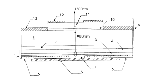
In the figure, the 1300 nm VCSEL made in accordance with the
principle of the invention comprises a conventional 980 nm VCSEL 1
acting as an optical pump and having a bottom mirror 2 of a
GaAs/AlGaAs quarte~avelength stack for 1300nm reflection, an
active medium 3 of InGaAs quantum wells confined between GaAs
layers or an AlGaAs alloy, and a top mirror 4 of a GaAs/AlGaAs
quarterwavelength stack. A backside contact 5 is formed on the
backside of the VCSEL 1 and isolation layers 6 are provided in a
conventional manner.

An intermediate GaAs buffer layer 7 is deposited on the top
mirror 4. The bottom mirror 8 of the main VCSEL 9 is grown on the
buffer layer 7. The bottom mirror 8 consists of quarterwavelength
stacks of gallium arsenide and aluminium gallium arsenide or alloys
thereof. The bottom mirror 8 is not shown to scale. In practice, it should
be about half the thickness shown. An active layer 10 consists of
indium gallium arsenide phosphide dots grown lattice mismatched to
the material of the bottom mirror 8. The quantum dots are embedded in
aluminium gallium arsenide or GaAs to form a quantum well.

The top mirror 11 consists of a stack of dielectric material such
as a silicon dioxide or silicon nitride based stack, or an airgap based
stack.

A ring-shaped contact 12 provides a field electrode. The mirror
1 1 is surrounded by a ground contact 13.

The above structure can be grown on a single substrate using
conventional techniques; i.e. MOVPE, metal organic vapor phase
epitaxy or MBE molecular beam epitaxy.

The 980 mn VCSEL diode 1 formed in the same structure as the
1300 nm VCSEL 9 acts as an optical pump to create a population

CA 02242670 1998-07-13


inversion at the active layer 10 of the main VCSEL 9. Since the
pumping VCSEL is part of the same structure, there is no need to
provide any optical elements to achieve good optical coupling.

The pump VCSEL 1, operating at 980 nm is activated by
applying a DC bias between its bottom contact 5 and the bottom mirror
8 of the main VCSEL 9 operating at 1300 nm.

The main VCSEL 9 is modulated by using an external electrical
o field applied perpendicular to the active layer 10, employing the
Stark-effect to deliberately change the bandgap of the active layer 10
and hence move the emission wavelength into and out of resonance
with the optical cavity formed between the top and bottom mirrors. The
optical output will therefore be modulated by the electrical field and not
as by injected carriers. The advantage of this arrangement is that the
1300 nm VCSEL will always be above threshold current so there is
less need to use a monitoring device.

The 1300 nm VCSEL 9 has a bottom mirror consisting of
aluminum gallium arsenide and its alloys. The active layer consists of
indium gallium arsenide phosphide quantum dots which maybe grown
lattice mismatched to the bottom mirror material. The quantum dots are
embedded in aluminum gallium arsenide or GaAs to form a quantum
well. The top mirror will consist of a stack of dielectric material, or
possibly air gaps.

The electrical field is supplied by contacts 12 on the top surface
and a contact 13 to the 1300 nm VCSEL bottom mirror, which may
serve as ground.

The complete structure described above may be grown in one
run and on one substrate and there is no need to fuse any of the
semiconductor layers.

CA 02242670 1998-07-13


Several variations of the invention are possibie. The invention
may apply to other semiconducting material systems, the mirrors may
both be dielectric, and in such a case the pump VCSEL top mirror may
serve as ground.

It may be possible not to use quantum dots for the active layer if
in the future homogenous 1300 nm active layers can be grown lattice
matched to gallium arsenide. Another variation is to grow or to fuse the
o 980 nm pump VCSEL onto an indium phosphide substrate containing
the 1300 nm bottom mirror and the active layers.

The invention meets the need for a 1300 nm light emitting
device that may compete successfully with traditional 1300 nm
edge-emitting laser diodes that are notoriously expensive.

The invention is applicable to other semiconducting material
systems. If no fusion is employed, the pump VCSEL top mirror may
serve as ground. The active layer can also consist of 1300 nm strained
InGaAsP quantum wells lattice matched to GaAs or AlGaAs.

If fusion is employed, the top layer may be made of InP with
InAs quantum dots or alloys thereof, or InP/lnGaAsP strained quantum
wells or alloys thereof. The top mirror is a dielectric. The bottom mirror
is an InP/lnGaAsP quarterwavelength stack, the InP buffer layer, and
the bottom VCSEL structure remain the same. Fusion is accomplished
between the InP and GaAs buffer layer.

Dessin représentatif
Une figure unique qui représente un dessin illustrant l'invention.
États administratifs

Pour une meilleure compréhension de l'état de la demande ou brevet qui figure sur cette page, la rubrique Mise en garde , et les descriptions de Brevet , États administratifs , Taxes périodiques et Historique des paiements devraient être consultées.

États administratifs

Titre Date
Date de délivrance prévu Non disponible
(22) Dépôt 1998-07-09
Requête d'examen 1998-11-04
(41) Mise à la disponibilité du public 1999-01-14
Demande morte 2002-07-09

Historique d'abandonnement

Date d'abandonnement Raison Reinstatement Date
2001-07-09 Taxe périodique sur la demande impayée
2001-07-18 R30(2) - Absence de réponse

Historique des paiements

Type de taxes Anniversaire Échéance Montant payé Date payée
Le dépôt d'une demande de brevet 300,00 $ 1998-07-09
Requête d'examen 400,00 $ 1998-11-04
Enregistrement de documents 100,00 $ 1999-01-19
Taxe de maintien en état - Demande - nouvelle loi 2 2000-07-10 100,00 $ 2000-05-09
Titulaires au dossier

Les titulaires actuels et antérieures au dossier sont affichés en ordre alphabétique.

Titulaires actuels au dossier
MITEL SEMICONDUCTOR AB
Titulaires antérieures au dossier
KULLANDER-SJOBERG, ANNA
WIDMAN, MICHAEL
Les propriétaires antérieurs qui ne figurent pas dans la liste des « Propriétaires au dossier » apparaîtront dans d'autres documents au dossier.
Documents

Pour visionner les fichiers sélectionnés, entrer le code reCAPTCHA :


Pour visualiser une image, cliquer sur un lien dans la colonne description du document. Pour télécharger l'image (les images), cliquer l'une ou plusieurs cases à cocher dans la première colonne et ensuite cliquer sur le bouton "Télécharger sélection en format PDF (archive Zip)" ou le bouton "Télécharger sélection (en un fichier PDF fusionné)".

Liste des documents de brevet publiés et non publiés sur la BDBC .

Si vous avez des difficultés à accéder au contenu, veuillez communiquer avec le Centre de services à la clientèle au 1-866-997-1936, ou envoyer un courriel au Centre de service à la clientèle de l'OPIC.


Description du
Document 
Date
(yyyy-mm-dd) 
Nombre de pages   Taille de l'image (Ko) 
Description 1998-07-13 5 207
Abrégé 1998-07-13 1 17
Revendications 1998-07-13 3 69
Dessins 1998-07-13 1 16
Abrégé 1998-07-09 1 16
Description 1998-07-09 4 172
Dessins 1998-07-09 1 16
Revendications 1998-07-09 2 50
Page couverture 1999-02-04 1 47
Dessins représentatifs 1999-02-04 1 8
Cession 1998-07-09 3 82
Poursuite-Amendment 1998-07-13 11 340
Correspondance 1998-09-22 1 30
Poursuite-Amendment 1998-11-04 1 32
Cession 1999-01-19 3 114
Poursuite-Amendment 2001-01-18 2 44