Sélection de la langue

Search

Sommaire du brevet 2243462 

Énoncé de désistement de responsabilité concernant l'information provenant de tiers

Une partie des informations de ce site Web a été fournie par des sources externes. Le gouvernement du Canada n'assume aucune responsabilité concernant la précision, l'actualité ou la fiabilité des informations fournies par les sources externes. Les utilisateurs qui désirent employer cette information devraient consulter directement la source des informations. Le contenu fourni par les sources externes n'est pas assujetti aux exigences sur les langues officielles, la protection des renseignements personnels et l'accessibilité.

Disponibilité de l'Abrégé et des Revendications

L'apparition de différences dans le texte et l'image des Revendications et de l'Abrégé dépend du moment auquel le document est publié. Les textes des Revendications et de l'Abrégé sont affichés :

  • lorsque la demande peut être examinée par le public;
  • lorsque le brevet est émis (délivrance).
(12) Brevet: (11) CA 2243462
(54) Titre français: OSCILLATEUR
(54) Titre anglais: AN OSCILLATOR
Statut: Réputé périmé
Données bibliographiques
(51) Classification internationale des brevets (CIB):
  • H03B 5/12 (2006.01)
  • H05B 41/282 (2006.01)
  • H05B 41/392 (2006.01)
(72) Inventeurs :
  • GREEN, IAN MACDONALD (Royaume-Uni)
(73) Titulaires :
  • CENTRAL RESEARCH LABORATORIES LIMITED (Royaume-Uni)
(71) Demandeurs :
  • CENTRAL RESEARCH LABORATORIES LIMITED (Royaume-Uni)
(74) Agent: RIDOUT & MAYBEE LLP
(74) Co-agent:
(45) Délivré: 2001-08-21
(86) Date de dépôt PCT: 1997-01-13
(87) Mise à la disponibilité du public: 1997-07-24
Requête d'examen: 1998-07-17
Licence disponible: S.O.
(25) Langue des documents déposés: Anglais

Traité de coopération en matière de brevets (PCT): Oui
(86) Numéro de la demande PCT: PCT/GB1997/000099
(87) Numéro de publication internationale PCT: WO1997/026705
(85) Entrée nationale: 1998-07-17

(30) Données de priorité de la demande:
Numéro de la demande Pays / territoire Date
9600982.4 Royaume-Uni 1996-01-18

Abrégés

Abrégé français

L'oscillateur faisant l'objet de la présente invention est capable de fournir à une charge, à partir d'un bloc d'alimentation en courant continu, de l'énergie à des fréquences supérieures à 100 kHz. Ledit oscillateur comprend une paire de transistors à effet de champ (16, 17) fonctionnant en opposition de phase dans un circuit résonnant et un limiteur de tension (35) qui, en cours d'utilisation, introduit un décalage de phase dans le circuit résonnant et renvoie l'énerge au bloc d'alimentation. Le limiteur de tension comprend de préférence un écrêteur à diodes couplé par induction au circuit résonnant. Un système d'entraînement avec modulation d'impulsions dans le temps pour lunette arrière sans électrode comprend un oscillateur de ce type, ainsi qu'un dispositif de commande marche-arrêt de l'oscillateur fonctionnant selon un schéma de modulation d'impulsions dans le temps.


Abrégé anglais


An oscillator, capable of delivering power from a d.c. power supply to a load
at frequencies above 100 kHz comprises a pair of field effect transistors (16,
17) operating in anti phase in a resonant circuit and a voltage limiter (35)
which in operation introduces a phase shift to the resonant circuit and
returns energy to the power supply. The voltage limiter preferably comprises a
diode clipper which is inductively coupled to the resonant circuit. A pulse
time modulation drive system for an electrodeless backlight comprises such an
oscillator together with control means for starting and stopping the
oscillator according to a pulse time modulation scheme.

Revendications

Note : Les revendications sont présentées dans la langue officielle dans laquelle elles ont été soumises.


4

CLAIMS:

1. An oscillator, capable of delivering power from a d.c.
power supply to a load at frequencies above 100KHz,
comprising, a pair of field effect transistors operating in
anti-phase in a resonant circuit, and a voltage limiter for
introducing a phase shift to the resonant circuit and
returning energy to the power supply, the voltage limiter
being inductively coupled to the resonant circuit.
2. An oscillator as claimed in claim 1, in which the
voltage limiter comprises a diode clipper.
3. A circuit arrangement, comprising an oscillator as
claimed in claim 1 or claim 2, means for starting the
oscillator in response to a first signal, and means for
stopping the oscillator in response to a further signal.
4. A circuit arrangement as claimed in claim 3 in which
the means for starting the oscillator comprises a
transformer magnetising inductance which resonates with the
input capacitances of the pair of field effect transistors
at a frequency above the oscillation frequency of the
oscillator in operation.
5. A pulse time modulation drive system for a discharge
lamp, comprising a circuit arrangement as claimed in claim
3 or claim 4 and control means for introducing said first
and said further signals to said circuit arrangement
according to a pulse time modulation scheme.

Description

Note : Les descriptions sont présentées dans la langue officielle dans laquelle elles ont été soumises.


CA 02243462 1998-07-17
WO 97/26705 PCT/GBg7/00099

AN OSCILLATOR

T'nis invention relates to an oscillator, and particularly, though not exclusively,
to an oscillator for driving electrodeless b7~k1ight~.
A number of low voltage oscillators have been described which use power
FETs (field effect tr~n~i~tors) as the active devices. The power supply voltage used is
t typically 12 or 28 volts.
A known characteristic of power FETs is their high input capacitance, which
must be charged and discharged on every clock cycle of the oscillator. As an
example, transistor type RFD14N05 (which is manufactured by Harris) has an on-
resistance of 0.1Q, and a m~xim-lm drain voltage of 50 volts, which suits it for use in
12 volt inverters or oscillators, supplying perhaps several tens of watts in a push-pull
configuration. However, the charge re~luired to switch on the gate of a single
RFD14N05 is typically 25 nanocoloumbs. If this charge comes directly from a +12
volt supply at the 10 M~Iz rate required for a 10 MHz inverter or oscillator, then the
gate drive power alone is 3 watts per transistor, or 6 watts per transistor pair.
As well as the difficulty of driving the gate electrodes, there is a further known
problem relating to the loop phase shift of self oscillating circuits. As is well known,
a stable oscillator has a loop phase shift which is either zero or an integral multiple of
2~. Since at 10 MHz there is a significant phase delay through the transistors, the gate
drive circuit has to incorporate a comF.on~t~ng phase advance, which must involve a
resistive loss. This in turn adds to the gate drive losses.
According to the invention, there is provided an oscillator, capable of
delivering power from a d.c. power supply to a load at frequencies above 100 kHz,
comprising a pair of field effect transistors operating in anti phase in a resonant
- circuit, and a voltage lirniter which in operation introduces a phase shift to the
resonant circuit and returns energy to the power supply. This arr~n~ement is very
simple and results in reduced gate drive losses.
The invention will now be described, by way of example only, with reference
30 to the accoll~allying drawing in which
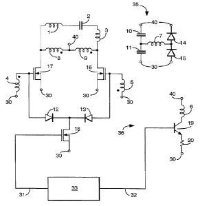
Figure 1 shows a circuit f~ m of a circuit arrangement according to the
invention.
The components shown in the Figure 1 are as listed in table 1 below.

CA 02243462 1998-07-17
WO 97/26705 PCT/GB97/00099


TABLE 1
Reference Number Component Type Rating/Serial Number
Inductive Load
2 Capacitor 100pf, 6kV
3 Transformer (1) Winding 1 turn
4 Transformer (1) Winding 3 turns
Transformer (1) Winding 3 turns
6 Transformer (1) Winding 3 turns
7 Transformer (1) Winding 3 turns
8 T~ r~ ller (2) Winding 7 turns
9 Tran~rull.. el (2) Winding 7 turns
Capacitor 47nf
11 Capacitor 47nf
12-15 Diodes BAT49
16-18 FETs IRL~ 014
19 Transistor 2N2222
Resistor 5 ohms

Transistors 16 and 17, together with adjacent components 2 - 11, 14 and 15
comprise the oscillator. Transistors 18 and 19, and components 12, 13 and 6, allow
the oscillator to be turned on and off at will. Apart from that, the latter components
take no part in the oscillation.
The component 1, as well as being an inductor, incorporates the load. In
practice, it consists of a spiral coil adjacent a glass b~ light envelope. Current in 1
causes a gas discharge in the envelope to strike, res~ll*n~ in the emission of light in
operation. Power absorbed by the load causes component 1 to have a correspondingresistive component.
Components 1 and 2 are automatically driven very close to resonance by the
phase shifts in the circuit, and thus define the ope~dting frequency. Feedback involves
the reactive component, capacitor 2, which feeds a current through reactive winding 3,
which in turn couples to 4, 5 and 7. The two transformers shown (one comprising
windings 3 - 7, the other of windings 8 and 9~ were bi-filar wound on 9.4 mm o.d.
toroids of 4C65 ferrite, manufactured by Philips. Other reactive components in the
feedback loop are the input capacitance of transistors 16 and 17, and the magnetising
inductance of the transformer having windings 3 - 7.

CA 02243462 1998-07-17
WO 97/26705 PCT/GB97/00099


Diodes 14 and 15 conduct on each half cycle of the oscillation, and return
oscillator energy to the power supply (the terminals labelled 30 in the Figure are
connected to the zero volt output of a d.c. power supply (not shown) whilst the
terminals labelled 40 are connected to the + 12 volt output). This causes a phase shift
in the gate wave forrns. Diodes 14 and 15 have a subsidiary function in that, due to
the transformer action of the transformer compri~ing components 3 - 7, they
effectively lirnit the gate drive voltage to transistors 16 and 17, thus protecting the
transistors. However, their primary function according to the invention is to provide a
phase shift. Components 10, 11, 7, 14, and 15 comprise a diode clipper circuit 35
10 being inductively coupled to the oscillator.
On initial start up, before the oscillator has entered the large signal mode
characterised by conduction of diodes 12 and 13, the circuit should oscillate atroughly the same frequency. This is ensured by arranging for the magnetising
in(l~lc~nce of the first transformer (3 - 7) to resonate with the input capacitance of the
15 two transistors 16, 17 at a frequency somewhat above the intended oscillator
frequency; the exact value is not critical.
Transistor 19 allows the oscillator to be started controllably, by applying a
positive going pulse of roughly 50 ns width to its gate. This injects current through 6,
thereby causing one of tr~n~i~tors 16 or 17 to turn on. Other ways of starting the
20 oscillator, such as biasing the gates of 16 and/or 17, will be obvious to one skilled in
the art.
Transistor 18 allows the oscillator to be stopped controllably. By applying a
positive level to the gate of 18, it turns on 18 and shorts the gates of transistors 16 and
17 to 0V.
This remote stop and start system is in~n~lerl for baclclight control, since
controlling the on/off ratio of the oscillator, at a repetition rate of perhaps 200 Hz,
conveniently controls the bri~htn~s~. In practice the brightness can be varied over a
range of at least 1000:1 using an appropliate pulse time modulation scheme. Control
means 33 is provided to introduce electrical control signals to the oscillator when it is
30 being used as part of such a pulse time modulation drive system for an electrodeless
discharge lamp. Such signals from outputs 32 and 31 switch the oscillator on and off
respectively as required.
Oscillator frequencies in the range 1 - 20 MHz are preferred, very preferably
in the range 5-15 MHz.


Dessin représentatif
Une figure unique qui représente un dessin illustrant l'invention.
États administratifs

Pour une meilleure compréhension de l'état de la demande ou brevet qui figure sur cette page, la rubrique Mise en garde , et les descriptions de Brevet , États administratifs , Taxes périodiques et Historique des paiements devraient être consultées.

États administratifs

Titre Date
Date de délivrance prévu 2001-08-21
(86) Date de dépôt PCT 1997-01-13
(87) Date de publication PCT 1997-07-24
(85) Entrée nationale 1998-07-17
Requête d'examen 1998-07-17
(45) Délivré 2001-08-21
Réputé périmé 2004-01-13

Historique d'abandonnement

Date d'abandonnement Raison Reinstatement Date
1999-01-13 Taxe périodique sur la demande impayée 1999-07-22
2001-01-15 Taxe périodique sur la demande impayée 2001-06-01

Historique des paiements

Type de taxes Anniversaire Échéance Montant payé Date payée
Requête d'examen 400,00 $ 1998-07-17
Le dépôt d'une demande de brevet 300,00 $ 1998-07-17
Enregistrement de documents 100,00 $ 1998-12-16
Rétablissement: taxe de maintien en état non-payées pour la demande 200,00 $ 1999-07-22
Taxe de maintien en état - Demande - nouvelle loi 2 1999-01-13 100,00 $ 1999-07-22
Taxe de maintien en état - Demande - nouvelle loi 3 2000-01-13 100,00 $ 1999-12-24
Taxe finale 300,00 $ 2000-10-03
Rétablissement: taxe de maintien en état non-payées pour la demande 200,00 $ 2001-06-01
Taxe de maintien en état - Demande - nouvelle loi 4 2001-01-15 100,00 $ 2001-06-01
Taxe de maintien en état - brevet - nouvelle loi 5 2002-01-14 150,00 $ 2001-10-15
Titulaires au dossier

Les titulaires actuels et antérieures au dossier sont affichés en ordre alphabétique.

Titulaires actuels au dossier
CENTRAL RESEARCH LABORATORIES LIMITED
Titulaires antérieures au dossier
GREEN, IAN MACDONALD
Les propriétaires antérieurs qui ne figurent pas dans la liste des « Propriétaires au dossier » apparaîtront dans d'autres documents au dossier.
Documents

Pour visionner les fichiers sélectionnés, entrer le code reCAPTCHA :


Pour visualiser une image, cliquer sur un lien dans la colonne description du document. Pour télécharger l'image (les images), cliquer l'une ou plusieurs cases à cocher dans la première colonne et ensuite cliquer sur le bouton "Télécharger sélection en format PDF (archive Zip)" ou le bouton "Télécharger sélection (en un fichier PDF fusionné)".

Liste des documents de brevet publiés et non publiés sur la BDBC .

Si vous avez des difficultés à accéder au contenu, veuillez communiquer avec le Centre de services à la clientèle au 1-866-997-1936, ou envoyer un courriel au Centre de service à la clientèle de l'OPIC.


Description du
Document 
Date
(yyyy-mm-dd) 
Nombre de pages   Taille de l'image (Ko) 
Page couverture 1998-10-26 2 54
Abrégé 1998-07-17 1 44
Description 1998-07-17 3 153
Revendications 1998-07-17 1 33
Dessins 1998-07-17 1 13
Revendications 2000-03-30 1 36
Page couverture 2001-08-07 1 37
Dessins représentatifs 1998-10-26 1 7
Dessins représentatifs 2001-08-07 1 6
Poursuite-Amendment 2000-02-22 2 3
Taxes 1999-07-22 1 36
Taxes 2001-06-01 1 38
Cession 1998-07-17 3 121
PCT 1998-07-17 12 320
Taxes 2001-10-15 1 31
Correspondance 1998-07-17 1 29
Cession 1998-12-16 2 83
Poursuite-Amendment 2000-03-30 3 83
Correspondance 2000-10-03 1 40
Taxes 1999-12-24 1 30