Note : Les descriptions sont présentées dans la langue officielle dans laquelle elles ont été soumises.
CA 02243492 1998-07-17
- WO 97/26Sl3I PCTlGB97/001i3
- - 1
This invention relates to optical devices.
~ Wavelength-selective optical fibre devices such as optical fibre gratings
are
commonly used in optical communication links. An example of this is the use of
a
chirped olstical fibre gratings connected to an aptical fibre link to provide
compensation against the dispersion of the optical fibre link.
Chirped fibre gratings are particularly useful in this type of application, as
they
are eompaca, passive and reiativcly simple to fabricate. It has been proposed
that the
lU dispersion compensation given by this technique wilt allow currently
installed step
index opti':,al fibre links to be upgraded to higher hit rates at, for example
a
wavelengtr~ of 1.5 hem (micrometers).
Chirped optical fibre gratings are inherently narrow-band devices, with a
dispersion-bandwidth product proportional to the grating's length. Two
conflicting
requirements then arise. Firstly, the dispersion of the grating must be
sufficient to
compensate; for that of the fibre Link, which in tum is generally proportional
to the
length of t:he fibre, link. Secondly, however, tha bandwidth of the grating
must be
sufficient riot only for the optical bandwidth of the signal being transmitted
via the
fibre link, but also to allow for inaccurate specification or icmparal drift
of the optical
ZU transmitter's centre wavelength.
The conflicting effect of these two requirements means that a grating I metre
Long would be required to provide a Snm (nanometrc) bandwidth and a dispersion
sufficient to compensate a i(lt)km (kilometre) link of currently standard
telecommunications fibre. However, current technology does not provide a
convenient
technique for fabricating such a Dong grating, and gratings of about one tenth
of this
length are .at the limit of present fabrication techniques.
It has been propascd that these problems can be av aidcd.if the grating is
made
to track the; transmitter's centre wavelength. This would allow a narrower
bandwidth
grating to be used, so increasing the dispersion available for a particular
grating
3U length. ('I'hc inverse of this proposal, where the transmitter is locked on
to the
grating, is undesirable in multiple-grating systems).
Previously proposed techniques far varying the wavelength response of a fibre
" .. _ . : ° ~,, .'. . ' ;~;~ ~,; ~s.~,
.. .._, . _..._. .. .. .-.. . ,.
i CA 02243492 1998-07-17
2
grating include stretching and compressing the grating using a linear
piezoelectric
transducer (PZT), or mounting the grating on a cantilever member which is then
bent
by a linear PZT attached to the free end of the cantilever member. However, in
the
linear PZT technique the grating is prone to buckling, and in the cantilever
technique
the orating will tend to become chirped (or an existing chirp of the grating
will
undesirably vary) as the cantilever bends.
US-A-4 703 287 discloses a -phase modulator formed by mounting an optical
fibre on a bimorph element.
This invention provides an optical device comprising an optical fibre grating
having wavelength-dependent optical characteristics mounted on a bimorph
element
operable to bend in response to an electrical control signal, so that the
wavelength-
dependency of the optical characteristics of the optical fibre grating vary in
response
to bending of the bimorph element.
By using a bimorph element in this way, a uniform compression or stretch (not
1~ easily obtainable with the cantilever technique) can be applied to the
optical fibre
grating, thus varying its wavelength-dependent properties but without
necessarily
changing the grating's chirp. The fibre can be securely fastened (e.g. glued)
to the
bimorph element along its length, avoiding the problems of fibre buckling.
Preferably the optical fibre grating is a chirped optical fibre grating.
Preferably the grating is apodised so that the modulation of refractive index
of the
fibre has a substantially cosine-shaped envelope.
In order to increase the amount of compression or stretching applied to the
fibre device, it is preferred that the bimorph element comprises more than two
active
layers of piezoelectric material. It is also preferred that the bimorph
element
comprises a plurality of active layers of piezoelectric material and an inert
buffer
layer disposed on the active layers, the optical fibre grating being attached
to the
buffer layer.
In order that the wavelength-dependent characteristics of the device can be
made to track those of, say, an optical transmitter, it is preferred that the
device
comprises a feedback control circuit for detecting whether the wavelength-
dependent
chara~~teristics of the optical fibre grating match those of a received
optical signal,
and, if not, for adjusting the electrical control signal so that the
wavelength-dependent
chara~~teristics of the optical fibre grating more closely match those of the
received
optical signal.
~;~n~~~sD s~~~T
CA 02243492 2004-08-27
3
In order to detect wavelength tracking errors and to determine an appropriate
direction for applying a corrective signal, it is preferred that the device
comprises means for
applying a dither signal to the electrical control signal, and/or the means
for detecting
comprises a wavelength-scanning optical monitor.
The invention also provides optical communication apparatus comprising: an
optical
transmitter; a dispersive optical fibre link; and an optical device as defined
above, the device
having a dispersion characteristic acting against the dispersion of the
optical fibre link.
Preferably the communication apparatus comprises an optical receiver for
receiving
optical signals transmitted via the optical fibre link; and the means for
detecting comprises
means for deriving an electrical signal indicative of the magnitude of the
output of the optical
receiver.
In accordance with one aspect of the present invention there is provided an
optical
device comprising an optical fibre grating having wavelength-dependent optical
characteristics mounted on a bimorph element operable to bend in response to
an electrical
control signal, so that the wavelength-dependency of the optical
characteristics of the optical
fibre grating vary in response to bending of the bimorph element.
In accordance with another aspect of the present invention there is provided
optical
communication apparatus comprising an optical device as defined in any one of
claims 1 to 8;
said apparatus further comprising: an optical transmitter; a dispersive
optical fibre link; and
wherein, the device having a dispersion characteristic acting against the
dispersion of the
optical fibre link.
The invention will now be described by way of example with reference to the
accompanying drawings, throughout which like parts are referred to by like
references, and in
which:
Figure 1 is a schematic diagram of a test apparatus incorporating a grating
according
to an embodiment of the invention;
Figures 2 and 3 schematically illustrate optical communication links using
such
gratings;
Figure 4 schematically illustrates a bimorph element;
Figure 5 schematically illustrates the bimorph element of Figure 3 when bent
in
response to an electrical control signal;
Figure 6 schematically illustrates the grating characteristics in open loop
operation
for three voltages of the electrical control signal; and
CA 02243492 2004-08-27
3a
Figure 7 schematically illustrates the grating characteristics in closed loop
operation.
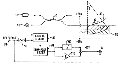
Figure 1 is a schematic diagram of a test apparatus incorporating a grating
according
to an embodiment of the invention.
In the test apparatus, a tunable laser source 10 supplies an optical signal
via a
coupler 20 to a grating 30. Light reflected from the grating 30 returns via
the coupler 20 to
an optical receiver 40.
The grating 30 is mounted on a bimorph element 50. The bimorph element
CA 02243492 1998-07-17
WO 97/26581 PCT/GB97/00113
4
-comprises a plurality of active picza electric (PZT) layers and iv operable
to bend in
response to an electrical control signal Vc. When the bimorph element SU
bends, the
fibre grating 30 is also bent and comprcssed/stretched and so the centre
wavelength
of the fibre grating is adjusted. '
S The fibre grating 3U in this embodiment is a ~Umm (millimetre) chirped fibre
grating constructed using a moving fibrc/phase mask-scanning beam technique
with
a cosinusoidal apodisation profile. This fabrication tcchniyue is described in
the
article "Moving Fibre/Phase Mask-Scanning Bcam Techniyuc for Enhanced
Flexibility
in Producing Fibre Gratings with a Uniform Phase Mask", Elcctmnics Letters,
Volume
1U 31, no. 17, August 1995.
At room temperature, the properties of the grating (when not bent) are as
follows:
3dB bandwidth - U.I3Snm
Peak reflectivity - 4fplo
1S Dispersion - -IIi~~Sps/nm
This dispersion is broadly eduivalcnt to the dispersion of lUUkm of standard
telecom fibre and the bandwidth is appropriate far a IUGbit/s transmission
system.
The grating is mounted on one side of the bimorph clement SU. For clarity,
the grating is illustrated flat against the bimarph clement S(D in Figure I,
and also in
2U a curved or bent position resulting from a bend of the bimorph element SU.
Because
of the way the grating is mounted on the bimorph clement, applying the comrol
voltage Ve to the bimorph element causes the grating to e.cpand or compress
uniformly, which tunes the central wavelength but leaves the chirp constant.
In the apparatus of Figure 1, an clcctrical feedback control circuit is used
to
2S allow the grating to actively track the transmitter wavelength (in Figure
1, for test
purposes, the transmitter wavelength is deliberately changed using the tunable
laser
10; in a real application, the transmitter wavelength could deviate with time,
temperature or a change of transmitter clcvicc).
In the feedback control circuit, an cicetricaE reference signal (i() is
supplied via
3U an ac (alternating current) modulator 7tD to a lock-in circuit Ht). The
lock-in circuit
8U also receives the output cmclopc of the optical receiver 4t) and generates
an error
signal indicating the difference between the reference signal and the output
of the
CA 02243492 1998-07-17
- WO 97/26581 PCT/GB97/00113
- 5
- receiver 4iJ. This error signal is IoW-pass filtcrccl by a filter c)t) and
is then supplied
to an intcf;rator It)t) and a scaling amplifier t 1 t), the outputs of which
are added to
generate a filter and scaled error signal i2t). This error signal 12t) is then
added to
the original reference signal Gt) to generate the control signal Vc for the
bimorph
clement.
Tha; purpose of the ac modulator 7t) is to add a small ac component to the
reference signal GO to provide a dither of the degree of bend of the bimorph
element
50. The dither is used to detect whether an improved response can be obtained
by
changing tI:c degree of bend of the bimorph element ~in either direction. In
the present
embodiment, the bimorph clement has a frequency response of up to about SOt)
Hertz,
so active locking is achievable at frequencies up to approximately this limit
(which
is generally much higher than the high frequency limit far the other
techniques
discussed in the introduction).
Figures 2 and 3 schematically illustrate optical communication links using a
bimorph-miounted grating and control circuit of the type Shawn in Figure 1.
In Figures 2 and 3, an optical transmitter 2t)t) generates optical signals
which
are eventually received by an optical receiver 24t), having been amplified by
an
amplifier 210, In the arrangement of Figure 2, the transmitter 2()t) supplies
the signals
directly to an optical fibre link (c.g. many kilometres long) .',SU, the
output of which
is then amplified and supplied to an optical circulator 22t). At one part of
the optical
circulator 22() is a grating 230 of the type described above, with associated
control
circuitry, and at the other port of the optical circulator is the receiver
24t). Figure 3
has a similar arrangement except that the grating 23t.) and optical circulator
220 are
positioned t>efore the optical fibre link 25U.
In each of the arrangements of Figures ? and 3, the bimorph-mounted grating
230 is used to compensate for the dispersion of the optical fibre link 25t),
while
tracking the: centre frequency of the optical transmitter 2t)t). In Figure 2,
the
equivalent ba the signal supplied by the optical receiver 4(1 in Figure 1 can
actually
be supplied by the optical receiver 24t), so that the optical receiver 240
itself also
3U supplies an c:nvclopc signal to the control circuitry far the bimalph
clement. In other
respects, thr, control circuitry may be the same as that Shawn in Figure 1. As
an
alternative, in Figure 3, tight which is not reflected by the grating 23t) can
be
CA 02243492 1998-07-17
- WO 97/26581 PCT/GB97/00113
- 6
monitored at the end of the grating 23t) not connected to the optical
circulator 22U by
a receiver 2Cn. Again, this can generate the envelope signal to be supplied to
the
lock-in circuit 8U, although in this Case the signal will have the opposite to
that
generated by the receiver 4U (i.e. it will be at it lowest if the grating is
perfectly
locked to the transmitter wavelength).
In a further alternative arrangement of Figure 3, the detector 2Ct) might be a
scanning optical detector such as a scanning Fabry-Perot device. The use of
such a
device can avoid the need for the dither signal supplied by the ac modulator
7U, as the
scanning detector can detect whether the grating would be better aligned to
the
IU transmitter centre wavelength for a small movement of the bimorph element
in either
direction.
Figures 4 and 5 schematically illustrate the bimorph element St) when not bent
(Figure 4) and when bent in response to the control signal Vc (Figure S).
It is desirable to obtain a small radius of curvature of the optical fibre
grating
IS 3U, to give a correspondingly large variation in the centre wav clength of
the grating
response. In one embodiment, this can be achieved by using a mufti-layer
bimorph
element (i.c. greater than two layers). Hawevcr, in the present arrangement to
be
described, the radius of curvature applied to the fibre grating 3t.) is
reduced by adding
an inert buffer layer 3UU in addition to the two or more activ a (Piezo
Electric) layers
ZU 31~ of the bimorph element. In effect, the buffer layer 3t)t) multiplies
the compression
or extension of the optical fibre grating 3t) from that which would be
obtained simply
be attaching the grating 3t.) directly to the uppermost active layer 3113.
This principle is illustrated in Figure 5, where the himorph element is shown
curved around a centre of curvature 32U. It can be seen that the radius of
curvature
r2 of the surface of the inert buffer layer is smaller than the radius of the
curvature
rl of the uppermost active layer 31t).
In the particular example used in a prototype apparatus, the active layers 310
were formed of a mufti-layer low voltage bimorph element such as an clement
sold
by Physik instrument GmbH under the part nee. PB14U.1(). The element is 45mm
Long
3U and t).8mm thick. By applying the csmtral voltage (Vc) at up to f3(1 volts
induces a
constant curvature along the device. Measured dt one end of the device, the
curvature
results in a maximum deflection of tt).5mm.
CA 02243492 1998-07-17
' WO 97l265li1 PCT/GB97/00113
7
Without the buffer layer, a maximum tuning r:rngc of t).Slnm was obtained.
By adding the buffer layer 30(), a tuning range of between l.7nm and snm has
been
obtained. The figure of l.7nm was obtained using a PVC buffer layer lmm thick.
Figure 6 iilustratcs the time delay and transn~issivity against wavelength for
the
grating 3U with three test voltages applied to the bimotph clement 5~ in an
open Ioop
configutati,on. The three test voltages were +3t) volts, t) volts and -3t)
voles. It can
be seen from Figure 6 that the different voltage tunes the central wavelength
of the
chirped grating but leaves the chirp rolativcly constant.
Figure 7 illustrates the response of the grating anti control circuitry in a
close
1Q loop configuration. This shows that the grating characteristics can be
maintained
relatively t:onstant over a tuning range of, in this example, about ().Slnm.
(Figure 7
was obtained in a prototype apparatus not using the buffer layer 3()0).