Note : Les descriptions sont présentées dans la langue officielle dans laquelle elles ont été soumises.
CA 02248372 2004-11-25
- 1
OPTICAL MULTI-CHANNEL SEPARATING FILTER WITH
ELECTRICALLY ADJUSTABLE PHOTON CRYSTALS
Description
FIELD OF THE INVENTION
The present invention relates to an optical multipath
switch composed of electrically switchable photonic
crystals.
RELATED TECHNOLOGY
Photonic crystals with band gaps are two-dimensional
and three-dimensional dielectric structures in which the
propagation of electromagnetic waves, in dependence upon, or
independent of, their direction of propagation, is forbidden
(see references 1 to 8).
Calculations and microwave measurements have shown that
cubic face-centred or also two-dimensional cubic
arrangements of holes in a dielectric matrix, or of
dielectric rods, exhibit such photonic band gaps (see
references 9 to 12).
As few as six planes suffice to ensure a high element
quality. Two-dimensional and three-dimensional structures
of this sort are often termed "photonic crystals." These
structures can be generated with high precision by means of
nanolithography using electron beam induced deposition. If
the cavities of such photonic crystals are filled with
nonlinear optical materials or liquid crystals and the
entire structure is exposed to a strong electrical field,
CA 02248372 2004-11-25
2
the optically active lattice constant in a crystal can be
set within certain limits by variation of the optical path
and hence the filtering effect of the element varied
electrically. A fabrication method which employs the
extended silylation process with dry etching, indiffusion
and subsequent element filling, allows the production of
highly integrated components at low cost.
Tunable filters used in optical communications and
telecommunications are implemented at present in the form of
long optical fibres whose filtering effect is created by
means of Bragg gratings inscribed in special fibres by
ultraviolet light (see references 13 to 17).
Fabricating such diffraction gratings with high
precision over appreciable lengths of several mm to cm is a
great technological challenge. Special procedures aim to
correct stitching errors which are commonly experienced in
electron beam lithography (see references 18 to 20).
Incorporation of fiber filters and fiber couplers into
a macroscopic optical arrangement needs be accomplished
using connectors or splices and a hybrid technology. A
miniaturization of components is not achievable in this
manner. The process called additive lithography uses
computer-controlled electron beam induced deposition to
build miniaturized photonic crystals, designed as two-
dimensional and three-dimensional arrangements of long
miniaturized needles, from dielectric materials with
nanometer precision (see reference 21).
These crystals can be inserted direct in the optical
path. High-precision computer control of the electron beam
in location, time and direction of motion enables the
generation of nearly all required crystal geometries and
their selective deformation needed to serve the intended
CA 02248372 2004-11-25
3
optical purpose. Thereby the optical behaviour of their
structure can be~tailored to meet the desired needs. By
filling the highly refractive needle structures with
nonlinear optical material (see references 22 to 24) or by
filling the highly refractive needle structures with liquid
crystals (see reference 25) and by applying a strong
electrical field to the filled structure, the optical path
in the crystal and hence its properties can be set
electrically. This allows the optical transmission
characteristic to be shifted finely, and the optical mirror
effect, the direction of reflection and possibly the
intensity to be varied. Since such elements possess both a
very high quality and a very small size (their dimensions
are only a few ~m in length, width and height), optical
devices and circuits equipped with such filters and mirrors
can be implemented with a high packing density.
In addition, solutions exist which use multibeam
writing systems with corpuscular beams. These solutions
permit optoelectronic devices and integrated optical
circuitry to be fabricated most economically by means of
additive lithography (see references 26 to 31).
SUMMARY OF THE INVENTION
It is an object of the present invention to provide a
low-loss switch arrangement based on electrically tunable
photonic crystals and hence providing a high packing
density.
According to the present invention, a two-dimensional
or three-dimensional photonic crystal is made from highly
refractive dielectric material using of electron beam
induced deposition. Photonic crystals with band gaps and
CA 02248372 2004-11-25
4
one or more narrowband transmission frequency ranges,
depending on their design, act as narrowband filters.
Calculations and microwave measurements have shown that
cubic face-centered or also two-dimensional cubic
arrangements of holes in a dielectric matrix, or of
dielectric rods, exhibit such band gaps. As few as six
planes suffice to ensure a high element quality.
The process called additive lithography is employed to
build two- and three-dimensional arrangements of long
miniaturized needles from dielectric materials with
nanometer precision, direct in the optical path. Owing to
high-precision computer control of the electron beam in
location, time and direction of motion, process allows the
generation of nearly all demanded geometries of crystals and
their selective deformation needed to serve the intended
optical purpose. This makes it possible to tailor the
optical behaviour of the crystal structure to meet the
desired needs. Similar structures can also be created by
means of nanolithographic procedures and the extended
silylation process using dry etching.
By filling the cavities between the needles with
nonlinear optical materials and placing the crystal in the
electrical field, the arrangement can be electrically tuned
within a certain wavelength range and adjusted with high
precision. Liquid crystal materials, which serve to fill
the structure, permit tunability of the filter over a broad
frequency range. By use of liquid crystals as fillers, the
filter is operable as a medium-velocity switch. In this
fashion, a switchable mirror can be constructed from a
crystal filled with nonlinear material.
A switch of the present invention is composed of
tunable photonic crystals. These crystals consist of long
CA 02248372 2004-11-25
miniaturized needles which act as high-precision optical
mirrors. Such needles serve to generate an optical geometry
in which deformations acting as photonic band gaps are
created selectively. The cavities between the needles are
5 filled up with nonlinear optical materials or liquid
crystals. By appropriate placement of electrodes in the
optical geometry, i.e., application of a strong electrical
field, the optical transmission characteristic of the entire
geometry can be changed up to reflection. Arranging further
l0 divided electrodes for separate control of the electrical
fields in individual crystal areas of the optical geometry
ensures that the optical geometry is at the same time
separately variable in individual crystal areas up to
reflection. Fixed photonic mirrors are placed directly in
the optical path at angles to the individual directions so
that the light can be coupled in and out through these
mirrors. In this way, an optical switch function is
performed by variation of the transmission characteristic of
the optical geometry in combination with the selective
coupling out of light via the individual fixed photonic
mirrors.
BRIEF DESCRIPTION OF THE DRAWINGS
Embodiments of the present invention are elucidated
below with reference to the drawings, in which:
FIG. 1 shows a schematic diagram of a tunable photonic
crystal which is used as a narrowband filter in a monomode
waveguide;
FIG. 2 shows a schematic diagram of a two-path
optically adjustable low-loss switch;
CA 02248372 2004-11-25
6
FIG. 3 shows a schematic diagram of a three-path
optically adjustable low-loss switch;
FIG. 4 shows a schematic diagram of an electrically
controllable multipath switch composed of a plurality of
three-path switches; and
FIG. 5 shows a schematic diagram of an electrically
switchable multipath switch.
DETAILED DESCRIPTION
FIG. 1 shows a schematic diagram of a tunable photonic
crystal which is used as a narrowband filter in a monomode
waveguide.
Based on this principle, an optically adjustable low-
loss, two-path switch can be designed, for example, as
illustrated in FIG. 2. To achieve this, a photonic crystal 2
having a critical geometry acting as a tunable mirror is
placed in the optical path between fixed photonic mirrors 4.
These mirrors are orientated such that the light is mirrored
at an angle of 22.5 degrees and hence hits the geometry of
the photonic crystal, which is filled with nonlinear
material 3 and acts as a tunable mirror, at a 45 degree
angle. If the geometry of the photonic crystal acting as a
tunable mirror is switched to transmission direction, the
light can pass unrestrictedly. When the geometry of the
photonic crystal acting as a tunable mirror is switched to
reflection the light is reflected exactly at the fixed
mirror, which couples the light into the connecting
waveguide 6.
Components of this kind find application in switching
networks and serve service selection purposes. The packing
density used in this technology is strongly increased
CA 02248372 2004-11-25
7
because the arrangement composed of mirrors and filter
switches is less than 12 ~m long and wide.
If the field plates 5 in the crystal area are
structured into four parts, a transmission and reflection
can be set in either half by alternate switching of the four
crystal quadrants 12, 14, 16, and 18 respectively. In this
manner a three-path switch 20 according to FIG. 3 may be
realized, the switch having an element with beam paths
orientated at 90 degree angles to one other.
By selective switching of transmission and reflection
in crystal areas between finer structured field plates, the
beam intensity can also be split up under electronic
control.
Another possibility for influencing the electrical
setting of the switch is to couple additional light into the
phot.onic crystal by means of a controllable light source
directed at the crystal filled with nonlinear optical
material. This allows fast switching in the upper gigahertz
range. In the process, the light can also be directed at
the waveguide light guidance plane from the space above or
below it. This renders guidance of the switching and the
switched light possible in separate planes.
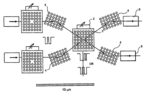
FIG. 4 represents schematically an electrically
controllable multipath switch 30 which has several three-
path switches 20 formed of photonic crystal areas 22 that
are separately tunable electrically and deflection mirrors
built from photonic crystals. This arrangement therefore
constitutes a cascaded coupler switch which consists of
miniaturized switchable four-path directional couplers made
from photonic crystals with an adjustable bandpass filter.
FIG. 5 shows the schematic diagram of an electrically
switchable multipath switch. The latter encompasses several
CA 02248372 2004-11-25
8
three-path switches 20 formed of photonic crystal areas 22
which are separately tunable electrically and thus
constitute a cascaded coupler switch which consists of
miniaturized switchable fourpath directional couplers with
an adjustable bandpass filter.
These devices can be combined with similar or different
integrated components--for example, mirrors, phase shifters
and reflectors--to build integrated circuits for optical
signal processing and optical computers with high packing
density. It is also possible to fabricate fixed or variable
measurement circuits serving to fulfill security functions
and to conduct data communication tests on optical fibers.
The present invention represents a novel electrically
controllable array of switches designed in integrated
technology and with high packing density. The present
invention serves to switch voltages and/or light between, or
to cross-connect, at least two optical paths. Through the
use of high-integration technology, little or no space is
required for insertion of the element into the optical paths
of, say, a computer circuit.
CA 02248372 2004-11-25
9
REFERENCES
1) John, Phys. Rev. Lett. 58, 2486 (1987).
2) Yablonovitch, Phys. Rev. Lett. 58, 2058 (1987).
3) L. McCall, P. w: Platzmann, R. Dalichacuch, D. Smith,
S. Schulz, Phys. Rev. Lett. 67, 2017 (1991).
4) M. Leung, Y. F. Liu, Phys. Rev. Lett. 65, 2646 (1990).
5) L. McCall, A. F. J. Levi, R. E. Slusher, S. J. Pearton,
R. A. Logan, Appl. Phys. Lett. 60, 289 (1992).
6) Yablonovitch, T. M. Gmitter, Phys. Rev. Lett. 63, 1950
(1989) .
7) Yablonovitch, T. M. Gmitter, K. M. Leung, Phys. Rev.
Lett. 67, 2295 (1991).
8) K. M. Ho, C. T. Chan, C. M. Soukoulis, Phys. Rev. Lett.
65, 3152 (1990).
9) S. Y. Lin, A. Arjavalingam, "Photon.ic Bound States in
Two-dimensional Photonic Crystals Probed by Coherent
Microwave Transient Spectroscopy", J. Opt. Soc. Am.
B/Vol. 11, No. 10 (1994), 2124.
10) S. Y. Lin, G. Arjavalingham, "Tunneling of
Electromagnetic Waves in Two-dimensional Photonic
Crystals", optics Letters, Vol. 18, No. 19 (1993), 666.
CA 02248372 2004-11-25
11) D. R. Smith, S. Schulz, S. L. McCall, P. M. Platzmann,
"Defect Studies in a Two-dimensional Periodic Photonic
Lattice", Journal of Modern Optics, Vol. 41, 2 (1994),
395.
5 12) C. C. Cheng, A. Scherer, "Fabrication of Photonic
Bandgap Crystals", J. Vac. Sci. Technol (1995),
Nov./Dec., to be published.
13) R. Kashyap, "Photosensitive Optical Fibers: Devices and
Applications", Opt. Fibres Techn. 1, pp. 17-34 (1994).
10 14) C. Cremer, H. Heise, R. Marz, M. Schienle, G.
SchulteRoth, H. Unzeitig, "Bragg Gratings on
InGaAsP/InPwaveguides as Polarization Independent
optical filters", J. of Lightwave Techn., 7, 11, 164
(1989) .
15) R. C. Alferness, L. L. Buhll, U. Koren, 2.j. Miller,
M. G. Young, T. L. Koch, C. A. Burrus, G. Raybon,
"Broadly Tunable InGaAsP/InP Buried Rib Waveguide
Vertical Coupler Filter", Appl. Phys. Lett. 60, 8, 980
(1992) .
16) C. Wu, C. Rolland, F. Sheperd, C. Laroque, N. Puetz,
K. D. Chik, J. M. Xu, "InGaAsp/InP Vertical Coupler
Filter with Optimally Designed Wavelength Tunability",
IEEE Photonics Technol. 4, 4, 457 (1993).
17) Z-M. Chuang, L. A., Coldren, "Enhanced Wavelength Tuning
in Grating Assisted Codirectional Coupler Filter", IEEE
Photonics Technology Lett., 5, 10, 1219 (1993).
CA 02248372 2004-11-25
11
18) H. W. P. Koops, J. Kretz, M. Weber, "Combined
Lithographies for the Reduction of Stitching Errors in
Lithography", Proc. EIPB 94, J. Vac. Sci. Technol. 3 12
(6) (1994), pp. 3265-3269.
19) B. H. Koek, T. Chisholm, A. J, van Run, J. Romijn,
"Sub 20 nm Stitching and Overlay for Nanolithography
Applications", Jpn. J. Appl. Phys., Vol. 33 (1994),
x.-.x.
20) V. V. along, J. R. Ferrera, N. J. Damask, H. I. Smith,
"Fabrication and Measurement of Highly Coherent
Electronbeam-written Bragg Resonators", Abstracts EIPB
'95, Scottsdale N3, 331 (1995).
21) H. W. P. Koops, R. Weiel, D. P. Kern, T. H. Baum, "High
Resolution Electron Beam Induced Deposition", Proc.
31st Int. Symp. on Electron, Ion, and Photon Beams, J.
Vac. Sci. Technol. B (1) (1988), 477.
22) M. Eich, H. Looser, D. Y. Ycon, R. Twieg, G. C.
Bjorklund, "Second Harmonic Generation in Poled Organic
Monomeric Glasses", J. Opt. Soc. Am. B, 6, 8 (1989).
23) M. Eich, A. Sen, H. Looser, D. Y. Yoon, "Corona Poling
and Real Time Second Harmonic Generation Study of a
Novel Covalently Functionalized Amorphous Nonlinear
Polymer", J. Appl. Phys. 66, 6 (1989).
24) M. Eich, G. C. Bjorklund, D. Y. Yoon, "Poled Amorphous
Polymers of Second Order Nonlinear Optics", Polymers
for Advanced Technologies, 1, 89 (1990).
CA 02248372 2004-11-25
12
25) R. Birenheide, M. Eich, D. A. Jungbauer, O.
HermannSchonherr, K. Stoll, J. H. Wendorff, "Analysis
of Reorientational Processes in Liquid Crystalline Side
Chain Polymers Using Dielectric Relaxation, Electro-
optical Relaxation and Switching Studies", Mol. Cryst.
Liq. Cryst., 177, 13 (1989).
26) H. Koops, 1974, German Patent Application P 2446
789.8-33, "Korpuskularstrahloptisches-Gerat zur
Korpuskelbestrahlung eines Praparates", U.S. Pat.
No. 4,021,674, granted on May 4, 1977.
27) H. Koops, 1974, German Patent Application 2 2460 716.7,
"Korpuskularstrahloptisches Gerat zur
Korpuskelbestrahlung eines Praparates", German patent
granted on Dec. 30, 1976.
28) H. Koops, 1974, German Patent Application P 2460 715.6,
"Korpuskularstrahloptisches Gerat zur
Korpuskelbestrahlung eines Padparates in Form eines
Flachenmusters mit mehreren untereinander gleichen
Flachenelementen", German patent granted on Oct. 31,
1979.
29) H. Koops, 1975, German Patent Application P 2515 550.4,
"Korpuskularstrahloptisches Gerat zur Abbildung einer
Maske auf ein zu bestrahlendes Praparat", German patent
granted on May 18, 1977.
30) M. Rub, H. W. P. Koops, T. Tschudi, "Electron Beam
Induced Deposition in a Reducing Image Projector",
Microelectronic Engineering 9 (1989), pp. 251-254.
CA 02248372 2004-11-25
~ 13
31) H. Elsner, H.-J. Doring, H. Schacke, G. Dahm, H. W. P.
Koops, "Advanced Multiple Beam-shaping Diaphragm for
Efficient Exposure", Microelectronic Engineering 23
(1994), pp. 85-88.