Note : Les descriptions sont présentées dans la langue officielle dans laquelle elles ont été soumises.
CA 02248517 1998-09-30
S279N3P072
SPECIFICATION
Manufacture of a microsensor device and a method for evaluating the
function of a liquid by the use thereof
The field of the Invention
This invention relates to a device for detecting a trace amount
of substance, particularly to a material recognizing device for
detecting a bio-molecular or other organic material or the like with
a high sensitivity and on a real time basis.
Related Art
A biosensor system as a means to monitor a biological function
instantaneously has been intensively studied and developed for
practical applications heretofore. The basic composition of a
biosensor consists of a section for detecting a biological substance
and a section for transducing a signal. A biological substance is
complexed with the recognizing component of the biosensor, and ensures
an ability to detect a bio-molecule, while the signal transducing
section transduces a change obtained through the detection of a
biological.substance into an electric signal. There are many kinds
of biological substances which can be detected on the basis of their
molecular properties, and they include enzymes, antibodies, binding
proteins, lectin, receptors, etc. What comes first includes
biological substances that have a molecule recognizing ability and/or
catalyzing function. They include enzymes, complex enzyme systems,
intracellular organelles, microorganisms, animal cells, plant cells,
etc. The catalytic activity of these substances depend on the
.structure characteristic with enzymes, and can be approximated, in its
1
CA 02248517 1998-09-30
S279N3P072
essence, by the kinetic equation by Michaelis and Menten. What comes
next includes substances that have a molecule recognizing function,
and forms a stable complex through a biological affinity. They include
antibodies, lectin, binding proteins, receptors, etc. The basic
designing of a bio-sensor proceeds with an attention paid to the above
properties. With the recent development of biotechnology, the range
of biological substances available for the biosensor has been widened,
and thus thermo-resistive enzymes, monoclonal antibodies or the like
come to be available. To convert the data obtained through molecule
io recognition into electric signals, physical parameter converting
elements such as electrochemical reactions, and an FET, thermistor,
piezoelectric element, surface elastic wave element, photodiode, etc.
have been utilized.
However, the above-described conventional biosensor devices have
is technical problems as described below. Firstly, the method for
producing a thin film for molecular recognition includes methods based
on photoresistance, electrochemical polymerization, manufacture of an
LB film, etc. The method based on photoresistance consists of forming
a photoresistant film on the entire surface of an ISFET (ion sensitive
20 field effect transistor), exposing only gate parts by lithography, and
forming a highly affinitive molecule recognizing film (organic film
or biomolecular film) on a gate insulating film. Then, the
photoresistant layer is peeled off to leave the molecule recognizing
film bonded to gate parts, which serves as a sensor. With this method,
25 however, it is difficult to neatly prepare minute dot electrodes on
the molecule recognizing film , and thus the incompletely finished edge
of dots results. A reduced yield occurs. Further, waste of materials
occurs as a result of lithography. Namely, 99% of photo-setting resin
2
CA 02248517 1998-09-30
S279N3P072
is discarded without being incorporated into actual products, that is,
the method causes a wasteful consumption of resources on earth, and
contamination of natural environments. This is a big problem. LB
technique (Langmuir-Blodgett's technique) is a method whereby a
mono-molecular film is formed on the surface of water, and the
film is transferred onto the surface of a solid substrate, and for the
method to be effective, it is necessary for the mono-molecular layer
to have a structure comprising hydrophobic and hydrophilic sections
in a balanced state. This method, however, is problematic in that the
io quality of LB film produced thereby is unsatisfactory in reliability:
the film has immeasurable flaws or pores thereupon, and does not allow
the formation of an uniform molecular film. Accordingly, with the
product manufactured by this method, it is difficult to distinguish
a change detected by a molecule recognizing film formed on an electrode
from a local change of the electrode.
Furthermore, the sensor film prepared by these methods is a
molecule recognizing film composed of one kind of molecule, which
recognizes only one kind of biological substance to which the film is
sensitive. Still further, it is impossible with these methods to apply
different biological substances simultaneously to a plurality of
electrodes. Thus, they are problematic in operability and detection
efficiency.
With a view to cope with above-described inconveniences, this
invention aims at introducing a method for producing a molecule
recognizing film distinct from the conventional ones, and further to
introduce a method being different, in the manner of detecting
biological substances, from the conventional ones.
3
CA 02248517 2006-10-25
Summary of the Invention
According to the invention there is provided a method of
manufacturing a sensor device comprising a circuit having organic
thin films formed on surface of microelectrodes forming a two-
dimensional array and a transducing element that detects change
in electric impedanace in connection with an electro-conductive
polymer, the polymer absorbing aromatic molecules, the method
comprising: printing a plurality of solutions of thin film
materials through a plurality of ink-jet nozzles simultaneously
onto the surfaces of the microelectrodes such that organic thin
films are formed on the microelectrodes, wherein each of the
plurality of solutions comprise an electro-conductive polymer and
a solvent, the electro-conductive polymer being different for
each of the plurality of solutions; the ink-jet nozzles each have
a piezo-electric element, the ink-jet nozzles being formed in a
multi-line head nozzle, and the solution has a viscosity of about
3 centipoise or less; the step of printing the solution of thin
film material comprises the steps of: (a) deforming the piezo-
elements by delivering an electric signal to the piezo-elements;
(b) ejecting the solution via the ink-jet nozzles to rest on the
microelectrodes, and (c) depositing the electro-conductive
polymer onto different regions of the two-dimensional array to
produce a device specific to a group of chemicals; and the
electro-conductive polymer of each solution consists of at least
one selected from the group consisting of, polythiophene,
polymethylethiophene, and polyphenylene vinylene. REPEAT CLAIM 1.
The electrodes and the circuit may be formed on a plastic
substrate.
The circuit may comprise poly-silicon thin film
transistors.
4
CA 02248517 2006-10-25
Brief Description of the Drawings
Fig. 1 gives a diagram to illustrate how minute electro-
conductive polymer electrodes are formed by the method of this
invention based on the use of an ink-jet.
Fig. 2 gives a diagram to illustrate how a functional solution
sample is analyzed by the methdd of this invention based on the use
of an ink-jet.
Fig. 3 gives a diagram to illustrate how a plurality of functional
solution samples are analyzed in a short period on electro-conductive
polymer electrodes by the method of this invention based on the use
2o of an ink-jet.
Fig. 4 is a block diagram to illustrate the principle underlying
the assay method of the microsensor device of this invention.
Fig. 5 gives an electronic circuit to collect data for analysis
using a microsensor device of this invention.
is Fig. 6 gives an electronic circuit to collect data for analysis
using another microsensor device of this invention.
Fig. 7 is a diagram to illustrate how sensor thin membranes having
various detection activities are formed on the microelectrodes of a
microsensor device of this invention.
Description of the Embodiment
The smallest embodiment necessary far representing the present
invention will be described below with reference to attached figures.
Figs. 1, 2, 3, 4, 5 and 6 give parts of interest to illustrate
the structure of a sensor device embodying the present invention. Fig.
1 gives a schematic view of an ink-jet head: 10 stands for an ink-
jet head; 11 for a head nozzle for ejecting ink droplets;'12 for an
electro-conductive polymer applied on the surface of an electrode; 13
5
CA 02248517 2006-10-25
for TFT miczoolectrodes; and 14 for suspended ink droplets ejected via
the ink-jet nozzle. The ink-jet head is driven by a piezo-electric
element activating mode, whereby, when an electric signal is delivered
from a driving circuit to the piezo-electric element, the piezo-
electric element is deformed; a liquid within is pushed out by the
deforming pressure; and the liquid is ejected via the nozzle.
In this case, the solution of an electro-conductive polymer is
ejected via the ink-jet nozzle as micro-dots, and the dots of polymer
solution in suspension are allowed to accurately reach the patterned
io microelectrodes to rest there. The usable electro-conductive polymer,
for example, includes polypyrrol, polymethylpyrrol, polythiophene,
polymetliyl.thiophene, polyaniline, polyphenylene vinylene, or the
like. Preparation of the solution of an electro-conduCtive polymer
requires more or less modifications according to the property.of the
polymer, because some polymers dissolve in organic solvents while
others do not. For an example take polypyrrol as the polymer of
illustration. A THF (tetrahydrofuran) solution of 0.30mmol pyrrol,
and another THF solution containing 0.25mmol phosphor monobutanate as
a catalyst and 30mg of plastisizer are introduced into respective
ink-jet tanks by nitrogen purge, and these solutions are ejected onto
microelectrodes. Dots composed of two different kinds of solutions
are.mixed on an electrode to form a mixture there; the mixture is
allowed to rest at room temperature for one hour to vaporize the
solvent; and a solidified polymer'thin film is formed there. Then,
the surface of thin membrane is washed with THF or methanol; and
residual solvent and unreacted monomers are removed. An electra-
conductive polymer soluble in the organic solvent is dissdlved in an
organic solvent to a concentration at which the solution has a
6
CA 02248517 2006-10-25
viscosity of 3cps or less, is then introduced in an ink-jet tank to
be ejected. To confer a selective absorbing activity to the
electro-conductive polymer, material including a specific type of
enzyme molecule or antibody chemically bound to the polymer,
s artificially synthesized molecule having similar recognizing function
to them, or material that a special type of enzyme molecule or antibody
is mixed into the electro-conductive polymer, are either dissolved in
the solution to give a homogenous solution. Micro dots of various kinds
of electro-conductive polymers resulting from polymer/enzyme or
io polymer/antibody mixtures are ejected via ink-jet nozzles to be
printed; the solvent is allowed to vaporize; and a biosensor film
results which carries an immeasurable number of sensor dots. Changes
in the electric impedance of, or in the electric current through
individual microelectrodes covered with respective electro- .
15 conductive polymers differ from each other according to the effects
exerted by films resulting from agglutination of bio-molecules such
as binding proteins, antibodies, DNAs, receptors, etc. adsorbed to the
surface, and thus to find what substance is on a given electrode dot
is easy. Fig. 2 gives a schematic view of the ink-jet to eject the
20 sample solution onto the surface of individual microelectrodes: 21
stands for the ink-jet head; 22 for nozzles; 23: for microelectrodes;
24 for sample solution; and 25 for suspended droplets of sample
solution. Zn the same manner by which the first molecule recognizing
films were formed on the electrodes, micro-dots comprising the sample
25 solution were ejected via the ink-jet nozzle into air and printed on
the molecule recognizing films made of an electro-conductive polymer.
By virtue of the biomolecular film thus formed on the eldetro-
conductive polymer, changes in electric impedance or in minute
7
CA 02248517 2006-10-25
electric current through individual electrodes are detected, which
allows a quick evaluation/analysis of a huge number of samples
For example, production of a patterned array of microelectrodes
is popsible by ejecting a plurality of electro-conductive polymer
solutions via a multi-line head nozzle into air, and thereby forming,
for example, ten different kinds of sensor dots each comprising several
hundreds line dots.
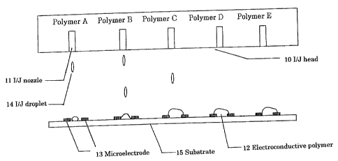
Fig. 3 is a diagram to illustrate how plural lines of dots
comprising different electro-conductive polymers are formed on the
io surface of a substrate like the one as used for the semiconductor
circuit board, to form a two-dimensional sensor, and how biological
sample dots are formed thereupon to be stabilized there. Assume, as
shown in the figure, in a crosswise direction, five different
electro-conductive polymers are placed one after another five times
is in repetition to produce 25 dots in total. These unit arrays are placed
in the same manner repetitively in the lengthwise direction to produce
a panel of 25 unit arrays which occupies practically the entire surface
of substrate. Upon this unit array of microelectrode sensor dots, this
time, five different kinds of biological samples are ejected via the
20 ink-jet nozzle in the crosswise direction one after another five times
in repetition until 25 micro-dots are suspended in air to fall onto
respective electrodes. Then, by monitoring changes in the adsorption
of biological material to the electrode, it is possible to
assay/evaluate the biochemical characteristics and responsiveness of
25 respective biological samples quickly on a real time basis, and
repeatedly and simultaneously. In this particular example, for each
of 25 different combinations, data comprising 25 measurements can be
obtained. As another example, let's assume a case where an array of
8
CA 02248517 2006-10-25
micro-dot electrodes comprising ten different kinds of electro-
conductive polymers is prepared, and ten different kinds of biological
samples are prepared so that they correspond with these dot.electrodes.
Then, simultaneous measurements based on 100 different combinations
become poesible. Assume that this forms a unit array, and that the
unit arrays are repeated five times to form the same panel as above.
Then, it is possible to obtain 25 times repeated measurements for each
of 100 different combinations
Then, the assay dependent on the use of a sensor device array
lo produced in the manner as described above will be described. Fig. 4
gives a simple block diagram of a circuit responsible for the assay
dependent on the use of a resistor sensor array. Principal functions
depicted in the figure are roughly represented by a resistor sensor
multiplex section, signal processing circuit section and pattern
recognizing section. Namely, the function depicted in this figure
consists of picking up signal from a single channel out of the
multi-channel resistors, and processing and recognizing it.
Accordingly, it is firstly important to accurately detect a change in
impedance.
The simplest and most accurate way of determining a resistance
includes various bridge methods, but these methods are not suitable
for measuring a change in resistance. An alternative method includes
a resistance to frequency conversion. This method, however, is
disadvantageous in that it is accompanied by noises, and requires a
rather long time for measurement. As one general method for detecting
a change in resistance, a circuit working on a voltage mode as shown
in Fig. 5 has been known. Tn this circuit, a specific type of iesistanee
sensor is chosen; a constant current is flowed through it; and the
9
CA 02248517 2006-10-25
voltage across the sensor is monitored. Then, as the voltage varies
in proportion to the resistance, it is possible to detect a change in
resistance by following a change in voltage. To determine changes in
resistance it is advisable to subtract the voltage given as a base to
the sensor by means of a differential amplifier, and then to amplify
the differential signal with a high-gain amplifier. The sensitivity
of the circuit depicted in Fig. 5 is proportional to the gain of
amplifier, and is given by the=following equation:
Vo = A ( I A-Vert ) ,
.io where (8Vo/8R,) = AIs,
An alternative method by which to detect a change in resistance
includes a method working on a current mode. Fig. 6 gives a circuit
diagram of the method. In this figure, a constant voltage is applied
to a resistor sensor chosen for this purpoee. To measure a change in
resistance, a constant current supplied from a source is flowed through
the sensor as an offset current; differences in current are removed
as a signal; and the signal is amplified. The sensitivity of the
circuit is proportional to the current gain of amplifier and to the
resistance of sensor.
IO õ +q,(Iotf-Vg/Ra )
where
(8To/5Rg) = A,/Ra' = AIs/RS
This type of current detection method commands a higher degree of
freedom than does the voltage detection method, and thus simplifies
the subsequent processing of signals.
Above-described semiconductor circuits are usually constituted
of field effect transistors (FET) arranged on a monocrystal silicon
substrate. However, because in recent years the function of thin film
CA 02248517 2006-10-25
transistors (TFT) formed on a polycrystal silicon (P-Si) film has made
a notable progress, it becomes possible to prepare this type of circuit
using polycrystal Si thin fi7m transistors (P-Si TFT). The P-Si TFT
has advanced so much that its'function is essentially equal to that
of monocrystal FET. Further, introduction of the method enabling the
manufacture of polysilicon at a low temperature allows the use of a
spacious glass substrate. This brings about a great cost-reduction
and a method that is suitable for the production of sensor devices like
the one of this invention.
TFT microelectrodes can be formed not only on a glass substrate
but on a thin plastic substrate having a softness and flexibility.
The TFT microelectrodes formed on such substrate can recognize
or act upon not only liquid samples, but various gas molecules and
volatile substances. Namely, individual volatile molecules are
adsorbed to the surface of electro-conductive polymers; the electric
resistance of electro-conductive films changes in association; and the
change is transformed into an electric signal for detection. For
example, the sensor device can be used for the recognition of ethanol,
acetone, harmful gases such as chlorine gas, cyanide gas, etc., or
vapours of aromatic molecules including perftunes and other odourants.
To be precise, this sensor device in film is left in an atmosphere
comprising a gas or vapour; the adsorbed gas molecule penetrates
through the surface of electro-conductive polymer into its interior;
and the entire polymer film changes its volume and/or other property
after undergoing expansions/Gont.ractions to cause changes in electric
resistance of the film. These changes are transformed into electric
signals for detection, and fed into a computer, and the infozutation
11
CA 02248517 2006-10-25
obtained through recognition thereof is available for a quick
feedback.
Several sensor arrays consisting of field effect TFTs could be
used for thesimultaneous identification, classification and
quantification of odours or other molecules. These sensors could be
used in conjunction with other sensors to detect chemicals. The TFT
sensors could be integrated onto a single device. Different
electro-conductive polymers are placed upon the gates of the TFT
sensors using ink-jet technology. in another modification the array
of TFTs could be constructed in a pattern to produce a two-dimensional
map of the odour response. The output from each TFT would then resemble
the output from a pixel of a CCD Camera. Different conducting polymers
could be deposited onto different regions of the array to produce a
device which was specific to a group or class of chemicals, e.g.
aromatics. When the molecules bind to or react with the polymer a
two-dimensional map corresponding to the particular odours will
appear.
The TFT cbip should include driving and reading electronics.
The information of the odour molecule could be read directly or
processed using for example neural networks or classical image
processing techniques to identify the odour molecules high
sensitively. The density and information of a special type of molecular
composition of different odours could thus be obtained.
Fig. 7 is a diagram illustrating how sensor thin films possessed
of various detection functions are prepared on the microelectrodes
formed on a sensor thin film: 71 stands for an electro-conductive
polymer film; and 72 for electrodes A and B. The size of each
microelectrode is preferably in the range of 1-100Jlm. The sensor is
12
CA 02248517 2006-10-25
stabilized on the polymer solution electrode which has been ejected
via an ink-jet nozzle, and converted to a thin film. A bio-molecule
or the like is adsorbed to the surface of this electro-conductive
polymer film; and a change in resistance or in current generated as
a result of the adsorption is monitored by the above-described
detection method.
Alternatively, a silicon-based, functional, surface modifying
solution is ejected via an ink-jet nozzle to be applied onto the surface
of a microelectrode, to form a silicone-based, functional molecular
io film there; a bio-molecule is chemically adsorbed to that film to cause
thereby electrons within to move towards the surface of electrode; and
therewith it is possible to gelectively detect the substance adsorbed
to the electrode surface. By the use of a device with basically the
same in composition with that as depicted in Fig. 7, that is, a,device
is wherein a silicon-based, functional molecular film is formed on an
electrode, and an electron-mobile protein moleculesuch as cytochrome
C is bound or adsorbed to that film, it is possible to monitor the
adsorption of protein to the surface of electrode by following minute
current changes resulting from electron transfer from the protein.
20 Or, it is possible to plate a gold thin film onto the surface of
a mi.croelectrode such that a thiol molecule and gold interact with each
other to form a self-organizing agglutination, which results in the
formation of a functional, monolayer film. The functional group
projecting from the surface of thiol monolayer which has been generated
25 as a result of self-assembly on the gold thin film plated on the
microelectrode has a function to selectively recognize a specific
bio-molecule or a volatile molecule. For example, as the functional
group projecting from the thiol molecule, a biotin derivative may be
13
CA 02248517 2006-10-25
used. A biotin molecule has a strong binding activity towards a
specific binding site of avidin or streptavidin, and its binding
constant is about 1415. This is practically the same as that encountered
in a covalent bond. To this biotin molecule film is transferred, for
example, a solution of avidin-ferritin binding protein via an ink-
jet nozzle. Then, avidin and biotin are selectively adsorbed; and the
ferritin protein molecule is stabilized on the electrode. The thus
selectively adsorbed molecule causes a change in refractive index of
the entire molecular film, and that change is captured as a change in
so dielectric constant of the adsorbing molecular film. Namely, it is
possible to convert the microelectrode into a polarized thin
film(capacztor), which serves as a sensor.
Advantage
According to this invention, provided is a method by which, in
contrast with conventional ones, a molecule recognizing film is
efficiently and in a short period formed on a microsensor in a uniform
and high quality manner. Further, according to this invention,
provided is a method by which to accurately introduce a vast number
of biological samples to be evaluated in a short period and efficiently
to plural, minute sensor electrode dots which have been prepared
according to said method for the formation of a molecule recognizing
film.
14