Note : Les descriptions sont présentées dans la langue officielle dans laquelle elles ont été soumises.
CA 02249790 1998-10-06
TITLE OF THE INVENTION
Method of alloying a noble-metal bypass layer of a high-
temperature superconductor
BACKGROUND OF THE INVENTION
Field of the Invention
The invention proceeds from a method of alloying
a noble-metal bypass layer of a high-temperature
superconductor in accordance with the preamble of patent
claim 1.
Discussion of Background
In the preamble of patent claim 1, the invention
makes reference to a prior art, such as is disclosed in
US-A-5,079,223. The latter specifies a method of produc-
ing a composite in which a high-temperature
superconductor is provided with a 30 nm - 100 nm thick
noble-metal layer of silver or gold or their alloys by
means of ion-beam evaporation or sputtering. Said
composite is joined to a metal substrate of copper or
aluminum or lead or zinc or their alloys by means of a
binder of In, Ga, Sn, Bi, Zn, Cd, Pb, Tl or their
alloys, which may form intermediate phases or solid
solutions with the noble metal, by pressing together at
a temperature of < 400~C (below the melting point of
said metals). No data are to be inferred from this
patent relating to the electrical resistivity of the
bypass layer obtained in this way to the high-
temperature superconductor.
It is known from JP 06-309955 A (in Patent
Abstracts of Japan) to impregnate silver-coated high-
temperature superconductors with a Pb-Sn solder.
It is known from US-A 4,914,081 to apply a metal
layer of silver or copper or tin or lead or zinc or
cadmium or indium or nickel or their alloys to a high-
temperature superconductor by electrolytic deposition.
CA 02249790 1998-10-06
- 2
EP 0592797 B1 discloses a method of producing a
rotationally symmetrical molding of a high-temperature
superconductor in which the metal, preferably of silver
or gold or of an alloy of these metals, introduced into
the fusion mold acts as a bypass with good conduction if
the high-temperature superconductor is to be used for
screening purposes. There are no data therein about a
method of alloying, for example, a silver fusion mold.
The use of an electrical bypass of pure noble
metal is unsuitable for a use of a high-temperature
superconductor as current limiter in alternating-current
lines, in particular for electrical powers of 2 1 MW,
since it is unsuitable for an economical current limita-
tion because of its low electrical resistivity, for
example, of 0.35 ~Q x cm at 77 K for silver. An electri-
cal bypass whose electrical resistance is less than that
of the high-temperature superconductor in the non-super-
conducting state would be desirable.
20SUMMARY OF THE INVENTION
Accordingly, one object of the invention, as it
is defined in patent claim 1, is to provide a method of
alloying a noble-metal bypass layer of a high-
temperature superconductor of the type mentioned at the
outset, with which the electrical resistivity of a
previously pure noble-metal bypass layer can be
increased by more than 10 times at a temperature of
77 K.
30Advantageous refinements of the invention are
defined in the dependent patent claims.
An advantage of the invention is that a high-
temperature superconductor of this type can be used as
current limiter in alternating-current lines.
35According to an advantageous refinement of the
invention, an increase in the electrical resistivity of
a previously pure silver bypass layer by 20 times can be
achieved.
.
CA 02249790 1998-10-06
.
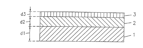
BRIEF DESCRIPTION OF THE DRA~INGS
A more complete appreciation of the invention
and many of the attendant advantages thereof will be
readily obtained as the same becomes better understood
by reference to the following detailed description when
considered in connection with the accompanying drawing,
wherein the sole figure shows a layer sequence of high-
temperature superconductor, noble-metal bypass layer and
alloy-metal layer before alloying.
DESCRIPTION OF THE PREFERRED EMBODIMENTS
Referring now to the drawing, in the sole
figure, a layer of a ceramic high-temperature
superconductor (1) which has a uniform superconductor
layer thickness (dl) is in good electrical and thermally
conducting contact with a noble-metal bypass layer (2)
which has a uniform bypass layer thickness (d2). Applied
to said noble-metal bypass layer (2) is an alloy-metal
layer (3) having a uniform alloy-metal layer thickness
(d3).
The high-temperature superconductor (1) is
preferably of the type: Bi2+xEA3Cu2Oy~ where -0.15 < x <
0.9, 8 < y < 8.3 and EA - an alkaline earth metal or a
mixture of alkaline earth metals, in particular a
mixture of Sr and Ca in the ratio Sr
Ca = (2 + z) : (1 - z), where 0 < z < 0.2.
The noble-metal bypass layer (2) to be alloyed
is preferably composed of silver (Ag). The alloy-metal
layer (3) contains lead (Pb) and/or bismuth (Bi) and/or
tin (Sn) and/or indium (In) and/or gallium (Ga) and/or
aluminum (Al) and/or mercury (Hg), preferably lead or
bismuth or gallium or aluminum.
The noble-metal bypass layer (2) is preferably
alloyed by diffusing the base-metals of the alloy-metal
layer (3) by means of a thermal treatment.
It is important that the high-temperature
superconductor (1) is adjusted to a superconductor laver
CA 02249790 1998-10-06
-- 4
thickness (dl) of < 500 ~m. The ratio of a bypass layer
thickness (d2) of the noble-metal bypass layer (2) to
the superconductor layer thickness (dl) should be
ad~usted to < 1/5.
It goes without saying that the desired alloy
can also be produced by ion implantation, but this is
associated with relatively high cost.
A bismuth layer having an alloy-metal layer
thickness (d3) of 0.5 ~m is applied to a noble-metal
bypass layer (2) of a silver foil having a bypass layer
thickness (d2) of 50 ~m:
a) by direct soldering onto the surface of the
silver foil (2) or
b) by immersing the silver foil (2) alone or the
layer sequence: high-temperature superconductor
(1) and noble-metal bypass layer (2) of silver
in a Bi or Bi/Ag bath at a temperature of 400~C
or
c) by sputtering Bi under vacuum or
20 d) by electrochemical deposition from a commercial
Bi-containing solution.
Said layer structure produced in this way is
then tempered at a tempering temperature in the
200~C - 400~C temperature range, preferably at 350~C, in
a pure nitrogen atmosphere for a tempering time of 1 h.
It is important that oxidation of the Bi is prevented
during this heat treatment.
Exemplary embodiment 1:
A 40 ~m thick silver foil (2) and a high-
temperature superconductor (1) with 20 ~m silver were
immersed in a hot bismuth bath at 400~C and then
tempered in a nitrogen atmosphere at 350~C for 1 h.
Cooling was then carried out slowly to room temperature.
The electrical resistivity of the alloy produced was
6.28 ~Q x cm at 77 K.
CA 02249790 1998-10-06
- 5
Exemplary embodiment 2:
A 1 cm wide and 20 ~m thick aluminum foil was
placed on a 2 cm wide and 50 ~m thick silver foil (2).
This was followed by a 1 hour tempering in a nitrogen
atmosphere at 650 C. The electrical resistivity of the
alloy produced was 8.8 ~Q x cm at 77 K.
Exemplary embodiment 3:
Silver foils (2) having layer thicknesses (d2)
of 20 ~m, 30 ~m and 50 ~m were coated with liquid
gallium so that they were then covered with an alloy-
metal layer thickness (d3) of 10 ~m. These 3 specimens
were tempered in air for 4 h at 90~C and then cooled.
The electrical resistivity of the alloy produced was
8.4 ~Q x cm and 5.0 ~Q x cm and 2.6 ~Q x cm,
respectively, in each case at 77 Ki it increased with
increasing tempering time and increasing tempering
temperature. If the 3 specimens were tempered at 450~C
for 4 h, their electrical resistivity was > 10 ~Q x cm.
Preferably, the alloy metal gallium is tempered at a
temperature in the 400~C - 500~C range for a time in the
1 h - 5 h range.
Obviously, numerous modifications and variations
of the present invention are possible in light of the
above teachings. It is therefore to be understood that,
within the scope of the appended claims, the invention
may be practiced otherwise than as specifically
described herein.