Note : Les descriptions sont présentées dans la langue officielle dans laquelle elles ont été soumises.
83(JSETR.L~OC CA 022~4~14 1998-11-26
"Switch for detecting the presence of a smart card in
a read/write device"
The present invention relates to a switch for detecting
the presence of a smart card, also called a contact-type
5 integrated-circuit card, in a read/write apparatus.
The invention relates more particularly to a switch of the
type having a body and means for controlling the switch, with
which means the front transverse edge of the card or the lower
face of the card engages.
Various designs of such a type of switch are known.
According to a first design, described and illustrated in
document EP-A-0,474,519, the control means are made in the
form of an eiastically deformable control blade, a free end of
which includes a ramp which is capable of engaging with the
15 front transverse edge of the card and which has an actuation
point which acts directly on the device for tripping the switch.
According to a second design, described and illustrated
in document EP-A-0,587,497, the control means include a lever
which is mounted so as to pivot on the switch and which has a
20 nose with which the front transverse edge of the card can
engage and a point for actuating the tripping device.
These designs have the drawback, in the read/write
position, of applying an elastic force to the card which urges it
towards the direction corresponding to extraction of the card,
25 this force having to be counteracted by complementary card-
braking means.
According to these designs, the value of the tripping
force applied to the tripping device is directly related to the
position of the card with respect to the control blade or to the
30 control lever, in the read/write position.
Document WO-A-95/33243 proposes a design of a
switch of the aforementioned type which makes it possible to
B305ETR.DOC CA 022~4~14 1998-11-26
remedy these drawbacks and according to which the control
means include an elastically deformable control blade, a first
end of which is embedded in a casing of the switch and the
second end of which engages with a device for tripping the
5 switch, and include a control lever which acts on the second
end of the control blade and which is capable of pivoting about
an axis parallel to the plane of the card in response to a
control force which is applied to it by the front transverse edge
of the card.
These various designs propose to make use of a
tripping device of convex general shape which is elasticaily
deformable in order to establish an electrical connection
between two electrical contacts of the switch in response to an
axial tripping force which is applied to it by the control blade,
S or by the control lever, in a direction approximatelyperpendicular to the plane of the card.
This type of tripping device is advantageous in that it
makes it possible to produce a switch assembly which is very
sensitive and which provides a sensation or tactile effect of the
tripping action.
However, the use of a tripping device consisting of an
additional component such as a monostable dome has the
drawback of increasing the thickness, or height, of the switch
and of increasing its cost.
It has already been proposed to produce the tripping
device in the form of another, stationary contact blade forming
part of the switch, but such a design requires this other blade
to be electrically connected to the printed-circuit board and, in
addition, again is laterally and/or longitudinally bulky and also
bulky heightwise.
B306ETR.DOC CA 022~4~14 1998-11-26
The object of the present invention is to provide a new
design of switch of the aforementioned type which makes it
possible to remedy these drawbacks.
To achieve this object, the invention provides a switch,
designed to be mounted on a printed-circuit board, for
detecting the presence of a smart card in a read/write
apparatus, of the type having a casing and means for
controlling the switch, with which means the front transverse
edge of the card engages, and of the type in which the control
o means comprise:
-an elastically deformable control blade, a first end of
which is embedded in a casing of the switch and the second
end of which engages with a device for tripping the switch; and
- a control lever which acts on the second end of the
control blade and which is capable of pivoting about an axis
parallel to the plane of the card in response to a control force
which is applied to it by the front transverse edge of the card,
characterized in that the control blade is a conducting
blade whose embedded first end is extended by a tab for
electrical connection to a conducting track on the printed-
circuit board and in that, in the presence of the card, the
second end of the control blade engages with another
conducting track on the facing upper face of the printed-circuit
board, which second end constitutes the device for tripping the
switch in order to cause electrical closure of the switch.
According to other characteristics of the invention:
- in the presence of the card, the control lever acts on
the second end of the control blade, against the resilience of
the blade;
- the control lever is made as one piece with the control
blade;
B30~ETR.D~:)C CA 022~4~14 1998-11-26
- the control lever has a control ramp with which the
front transverse edge of the card engages;
- the control blade is approximately plane and extends
longitudinally in a direction approximately parallel to the
5 direction of insertion of the card;
- the control blade is shaped like a hairpin with two
branches which extend in a direction approximately parallel to
the direction of insertion of the card, which are connected by
an approximately 180~ bend and among which the end of an
10 upper first branch is embedded in a casing of the switch and
the free end of the lower second branch is capable of engaging
with the said other conducting track on the printed-circuit
board;
- the lower second branch is extended beyond the said
S free end by at least one tab for vertical positioning of the
control blade at rest;
- the second end of the control blade, which is capable
of engaging with the said other conducting track, has a convex
contact part whose convexity is turned towards the upper face
20 of the printed-circuit board;
- the control lever is mounted so as to pivot about an
axis approximately perpendicular to the direction of insertion of
the card;
- the first end of the control blade is embedded in the
25 material of the casing of the switch;
- the first end of the control blade is fixed into one
element of the casing of the switch by hot riveting.
Other characteristics and advantages of the invention
will appear on reading the following detailed description which
,o may be understood by referring to the appended drawings in
which:
B30.ljETRLOC CA 022~4~14 1998-11-26
- Figure 1 is an isometric perspective top view of a first
embodiment of an electrical connector having a switch
according to the teachings of the invention;
- Figure 2 is an isometric perspective bottom view of the
assembly shown in Figure 1;
- Figure 3 is an isometric perspective top view of the
switch element forming part of the assembly shown in Figures
1 and 2;
- Figure 4 is an isometric perspective bottom view of the
o element shown in Figure 3;
- Figure 5 is a detail, in cross-section on the line 5-5 in
Figure 1, in which the switch is illustrated in the rest position;
- Figure 6 is a view similar to that of Figure 5, in which
a smart card has been shown in the process of being inserted,
the card bearing on the upper guiding face of the insulating
support, and in the position corresponding to the moment at
which the switch changes state, but with a zero contact
bearing force;
- Figure 7 is a view similar to that in Figure 6, in which
the smart card is shown in the position in which it is fully
inserted longitudinally;
- Figure 8 is a view similar to that in Figure 7, in which
the card is shown in its maximum raised position with respect
to the upper face of the insulating support;
- Figures 9 to 16 are views similar to those in Figures 1
to 8, which illustrate a second raised embodiment of the
assembly illustrated in Figures 1 to 8; and
- Figures 17 to 19 are three views similar to those in
Figures 1, 2 and 3, which illustrate another embodiment of a
switch according to the teachings of the invention.
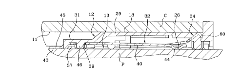
Figures 1 to 8 show an entire connector 10, having a
built-in switch 12 for detecting the presence of a smart card C,
B306ETR.~OC CA 022~4~14 1998-11-26
also called a chip card, and incorporating end-of-travel stop
means for insertion of this card C in the direction 1.
The connector 10 is designed to be mounted on a
printed-circuit board P (see Figures 5 to 8) of a read/write
apparatus (not shown), the read/write apparatus having its own
means for guiding the card C during its insertion and optionally
means for positioning the card C relative to the entire
connector 10 which press on the card vertically.
The main part of the connector 10 illustrated in Figures
o 1 and 2 essentially consists of a support 16 made of a moulded
plastic insulating material.
According to a known design, which is illustrated in
document WO-A-95/33243 for example, the support 16
essentially consists of a horizontal plate which delimits a plane
upper face 18 serving as a support for a plurality of elastically
deformable electrical contact blades 20 which project into slots
22 formed in the support 16, the lower face 24 of which bears
vertically, with regard to Figure 6, on the upper face 13 of the
printed-circuit board P.
The contact blades 20 project from the upper face 18 of
the support 16 in order to come into contact with the
corresponding conducting areas on the card C and they are
extended, in this embodiment, at the lower face 24 of the
support 16, in the form of bent connection tabs 28 intended to
be soldered to the conducting tracks on the upper face 13 of
the printed-circuit board P, for example using the known
technique of surface-mounting components.
The outputs 28 may also be pinned to the conducting
areas of the printed-circuit board P or may simply be elastically
held in bearing contact therewith.
B30~5ETR.~OC CA 022~4~14 1998-11-26
The support 16 has a rectangular general outline and it
includes an adjacent extension 29 which is moulded as one
piece with the support 16.
The extension 29 serves as a support to the main
components of a switch 12 for detecting the presence of the
card C and it is adjacent to one of the longitudinal edges 30 of
the main part of the support 16, parallel to the direction of
insertion 1.
The extension 29 is moulded as one piece and its
thickness is reduced at the rear in order to form a step 31
allowing passage for raised parts, for example etched parts,
formed on the corresponding part of the lower face 11 of the
card C.
The upper face 18 of the support 16 is a continuous
s plane face which also constitutes the plane upper face of the
extension 29.
This plane upper face 18 is capable of forming a
bearing face on which the lower corresponding face of the card
C can slide.
The built-in switch 12 essentially consists of a switch
element 33 which is an element cut and folded from a sheet of
electrically conductive material.
The switch element 33 is placed in a housing 35
accessible from the lower face 47 of the extension 29,
coplanar with the lower face 24 of the support 16, in which it is
held by three studs 46 arranged in a triangle which extend
vertically downwards in order to pass through corresponding
holes 39 formed in a rear heel 37 of the element 33 and the
free ends of which are hot- crimped so that the body of the
switch element 33 extends longitudinally forwards in the
manner of a beam, the rear end 37 of which is embedded in
the support 16, 29.
B3û6ETR.DOC CA 022~4~14 1998-11-26
The heel 37 is extended rearwards by a bent connection
tab 43 which is designed to be soldered to a first conducting
track 45 on the upper face 13 of the printed-circuit board P
associated with the electrical switching function.
5The switch includes, according to the teachings of the
invention, a conducting control blade 32 forming part of the
switch element 33, which extends longitudinally forwards,
approximately in the horizontal plane of the heel 37, inside the
housing 35 and which inciudes, near its free second end 42, a
oconvex part 44 whose convexity is oriented vertically
downwards .
At rest, as may be seen in Figure 5, the lower face of
the convex part 44 extends a short distance, for example
0.25 mm, from the lower face 24, 47 of the support 16, 29 and
15therefore from the upper face 13 of the board P.
The free end 42, 44 extends vertically in line with
another conducting track 26 on the upper face 13 of the board
P associated with the electrical switching function.
When the free end 42, 44 comes into contact with the
20conducting track 26, the control blade 32 then establishes an
electrical connection between the tracks 45 and 26, that is to
say that it closes the switch 12, which is a switch of the
normally-open type.
Within the context of the invention, the conducting track
2526 is therefore an element for tripping the switch with which
the control blade 32, 42, 44 engages when the switch is
actu ated .
For this purpose, and according to a design known from
document WO-A-95/33244, the control blade 32 is elastically
30deformable in the manner of an elastic beam due to the action
of the forward or front transverse edge 50 of the card C which
B306ETR.DOC CA 022~4~14 1998-ll-26
acts on a control lever 34, or actuation lever, for actuating the
deformation of the control blade 32.
The control lever 34 forms part of the switch element
33. It acts on the control blade 32 with which it is made as one
s piece.
In fact, as may be seen in particular in Figures 3 and 4,
the control lever 34 is in the form of a longitudinal arm 64
which is adjacent to the main part 40 of the control blade 32 to
which it is connected approximately laterally half way along it
o by an elbow 66.
The front free end 60 of the control lever 34 is shaped
as a "control pedal". For this purpose, it has an inclined control
ramp 58 and projects beyond the upper face 18 through a hole
61 in the horizontal upper plate of the support 16.
Near its elbow-shaped rear connection end 66, the
control lever 34 has a flexing region 62.
In the same way, the region 38, connecting the control
blade 42 to the embedment heel 37, constitutes a flexing
region forming a transverse pivot pin for the switch element 33,
this pivot pin being parallel to the plane of the card C and
perpendicular to the direction of insertion.
When the user inserts a card C into the read/write
apparatus, the front transverse edge 50 of the card C (Figure
6) engages with the portion 58 of the control lever 34, this end
portion 58 forming an approximately 45~ ramp, and causes
general pivoting of the assembly comprising the control lever
34 and the control blade 32, 40 substantially about the curved
connection portion 38 which causes the switch to trip because
of contact of the convex part 44 with the tripping track 26.
This deformation occurs gradually as soon as the front
transverse edge 50 of the card C engages with the ramp 58,
the continuation of the insertion force subsequently causing
B306ETRDOC CA 022~4~14 1998-11-26
partial flexure of the control lever 34 with respect to the
general plane of the main body 40 and of the arm 64 of the
control blade 32 about the region 62, that is to say about a
flexure axis approximately perpendicular to the direction I (see
Figure 7).
By virtue of this flexing phenomenon, and in the
inserted position of the card, the ramp-forming portion 58 lies
below the lower face 11 of the card C without in this case
applying any force to the card C against the insertion force.
o When the user removes the card C, and because of the
intrinsic resilience of the control blade 32 and of the arm 64
forming the control lever 34, these elements resume their
position illustrated in Figure 5.
As has just been explained, the control lever 34
actuated by the front transverse edge 50 of the card C is
mechanically uncoupled from the second end 42 of the control
blade 32.
The high travel which results therefrom and the
possibility of a significant overtravel for the control lever 34
make it possible, by a reduction effect, to reduce the actuation
force applied by the front transverse edge of the smart card
substantially, this being an ergonomic advantage from the
user's standpoint and which is, above all, advantageous in
terms of wear of the smart card, which generally is made of a
soft plastic and is subjected to a large number of operations.
This high travel of the control lever 34 also makes it
possible to absorb any differences in position of the smart card
with respect to the plane of the upper face 18 of the insulating
support 16 (see Figure 8) without causing substantial
differences in the switching time because of the short travel of
the contact and bearing point 44.
The design according to the invention:
B306ETR.DOC CA 022~4~14 1998-11-26
- allows a high overtravel of the control lever 34 (of the
order of 1 mm, approximately) while the travel of the convex
part of the point 44 which bears on the contact pad 26 of the
printed-circuit board P is about 0.25 mm; and
- prevents large variations in the force bearing on the
contact pad 26 depending on the vertical distance separating
the lower face 11 of the smart card C from the upper plane of
the insulating support of the connector 16, which distance can
vary between 0 and 0.35 mm, depending on the tolerances on
o the thickness of the smart card (i 0.08 mm) and on the system
for guiding the latter, within which range of variation the force
bearing on the electrical contact 26-44 reaches the value
necessary and sufficient to guarantee good quality of the
electrical contact.
The advantages of the design according to the invention
are as follows:
- there is only one semi-permanent electrical contract
point (instead of 2 usually) and therefore a more robust
design;
- extreme simplification by combining all the functions
into a single piece 33, thereby making it possible to minimize
its manufacturing cost and to simplify the assembly processes,
and therefore also to minimize the investment costs, something
which is very important when it is desired to integrate the
25 switching function in many different versions of a smart-card
con nector;
- miniaturization of the switching function, making it
possible to respond to new applications requiring products with
a very small total thickness and with a very small area
30 occupied on the printed circuit;
- soldering the connection tab 43 connected to the
"embedded" first end 47 of the control blade 32 also ensures
B306ETR.DOC CA 022~4~14 1998-11-26
that the component is mechanically fixed to the printed-circuit
board P, which may prove to be very useful for certain
connector configurations;
- mechanical protection of the electrical contact point
5 26, 44 by virtue of the structure of the insulating plastic
casing-forming support 16, 29 of the switch 12 in a housing of
which structure the switch element 33 with its control blade 32
is mounted, that is to say protection against unfortunate
handling operations, but also, to a certain extent, protection
o from pollution by foreign bodies or from dust since the opening
68 in the casing 29 allowing passage for the pedal 58, 60 of
the control lever does not lie above the contact point 26, 44
and since the concave enlarged upper face of the convex part
44 constitutes a second level of mechanical protection above
15 the contact point.
The drawback over the prior solutions using a tripping
element of the bistable-dome type, which is that there is not
complete sealing of the contact point, is compensated for by
certain of the above technical advantages: more robust design
20 and protection provided by the configuration of the casing.
Moreover, the purpose of this design is not to be a
substitute for those of the prior art which are described in
documents WO-A-95/33244 and WO-A-95/33243 but to
complement them in order to respond to other requirements for
25 which the cost and miniaturization outweigh the lifetime and
reliability.
Moreover, the fact that the contact pad 26 on the
printed-circuit board is preferably gold-plated for this simplified
switch version is not a troublesome constraint for applications
30 of this type in which all the conducting tracks of the printed
circuit are already gold-plated because of the technology
employed for surface-mounting the other components.
B306ETR.OOC CA 022~4~14 1998-11-26
Another indirect advantage of the design according to
the invention is the configuration of the support 16, 29 forming
the casing, which makes it possible, without modification other
than the addition of a small switch and of a control lever
without a connection tab, to obtain a version similar to that
described in documents WO-A-95/33244 and WO-A-95/33243.
This advantage may thus guarantee the possibility of users
changing over to a "sealed" solution or, on the contrary, to a
"low-cost" solution, depending on the initial choice, without the
o mechanical modification of his equipment or of his assembly
processes, the sole precaution to be taken being to produce,
on the printed circuit, a double implantation at the tracks 26
and 45 connected to the switch 12, 33.
The second embodiment illustrated in the figures is a
so-called "raised" connector necessary for some applications,
for example when the upper face 13 of the printed-circuit board
P is partially encumbered by other components.
In order to adapt the design according to the invention
described previously with reference to Figures 1 and 8, and as
may be seen in Figures 9 to 16, it was firstly necessary to
adapt the connection tab 43 by increasing the height of it, like
that of the connection tabs of the contact blades of the
connector 10.
Moreover, the design of the active part of the resilient
and conducting contact blade has been modified in order to
adopt a hairpin configuration as the vertical distance
separating the convex contact point 44 from the track 26 varies
with the height of the connector and of the casing 29 of the
switch 12.
The hairpin design makes it possible, by virtue of the
opening between its upper branch 40S and lower branch 401,
to adapt the control blade 32 to the height of the insulating
B3n6ETR.30C CA 022~4~14 1998-11-26
14
support 16, 29 by a simple adjustment of the tool for bending
the control blade 32 with the two branches 40S and 401.
As may be seen in particular in Figures 11 and 12, the
upper branch 40S of the control blade 32 extends
longitudinally forwards from the heel 37 and is extended by a
front elbow or bend 70 which itself connects the lower branch
401 which extends longitudinally rearwards as far as its free
end part 42 which has the convex part 44.
In order to position the convex part 44 very precisely in
o the rest state and to take into account the substantial
reduction in the vertical bearing contact force resulting from
the elongation of the contact blade 32, the free end of the
lower branch 401 is shaped in the form of a "T", that is to say
that it has two opposed transverse tabs 72 which constitute a
bearing bar 74 and which bear on the lower end faces 76 of
two columns 78 moulded with the support 16, 29 and which
extend vertically downwards. This arrangement, as may be
seen in Figure 13, allows the convex part 44 to be precisely
positioned with respect to the contact pad 26.
When the card C actuates the control lever 34, the
bearing points formed by the lower ends 76 of the columns 78
exert a magnifying effect on the bearing contact force of the
convex part 44 on the upper face 13, 26 of the printed-circuit
board P, preventing the free end of the lower branch 401 of the
control blade 32 from rising in order to obtain a bearing
contact force equivalent to that in the first embodiment.
The embodiment illustrated in Figures 17 to 19, in which
a connector of the type described and illustrated in document
EP-A-0,738,983 is shown, will now be described.
As may be seen in particular in Figure 19, the width of
the connection tab 43 has been reduced in order to allow it to
be infrared-reflow soldered through one 202 of the
B3(~6ETR.OOC CA 022~4~14 1998-11-26
standardized openings (for testing the connector) in the metal
cover 200 of the connector. The reflow beam, after having
passed through the opening 202, then passes through a hole
204 in the insulating support 16, while the control pedal 60
5 extends through a hole 41. This design avoids having to use
too long a tab 43.
.... . . .. . .