Note : Les descriptions sont présentées dans la langue officielle dans laquelle elles ont été soumises.
CA 02263769 1999-02-l9
W O 98/08366 PCT/SE97/01371
PROTEC~VESHnELD OF EMC-TYPE
Technical field
The present invention relates to a surf~ce-mounted protective sh~eld for components
5 on e.g. a circuit board.
State of the art
The screening of components on circuit boards is becoming more important, espe-
cially in the case when the signal speed approaches the Gbit region. It is well known
10 that radiation from certain components at high frequencies can cause interference
with communications e.g. telecomrnunication. This phenomenon is called RFI, radio
frequency interference. The interfering circuits can either be shielded with closed
boxes or the sensitive components can be shielded with closed boxes in order to
prevent interference.
In GB 2 226 187 there is described a mini~hlre protective shield for eleckonic com-
ponents arranged on a circuit board. The protective shield comprises a number ofcontact springs and a lid. The contact springs are arranged around the componentand are in electrical contact with the circuit board. The contact springs are in general
20 U-shaped. The lid comprises a flat surface with side walls along all the edges so that
the lid is similar to an open box. The size of this box is adapted to the contact
springs on the circuit board. The sides are intended to be inserted into the U-shaped
contact springs so that a protective shield is formed.
In WO 95/28074 a contact spring is described which can be used to connect a pro-tective shield to a circuit board. This contact spring has a different appearance com-
pared to the above mentioned contact springs, which means that the contact between
lid and contact spring is ensured and that the shielding increases.
The problem ofthe above contact springs is that they are ~uite complicated to
arrange around the component on the circuit board. This solution is, filrthermore,
CA 02263769 1999-02-l9
W O 98/08366 PCT/SE97/01371
not completely optimal, both with regard to space requirements and the degree ofprotection.
Disclosure of the invention
5 On circuit boards where certain components produce much electromagnetic radia-tion, the placement of these components must be chosen with great care so that the
radiation shall not cause operational problems. On e.g. a single-sided circuit board,
where both a transmitter and a receiver are placed, the minimum size of the circuit
board is limited to how near each other the transmitter and receiver can be placed
10 without causing operational disturbances.
A problem which occurs when different products tend towards smaller and smaller
dimensions is that the screening between sensitive components must be increased.
15 Another problem is that known protective shields take up too much room and are
complicated and time-consuming to place on the circuit board, either because they
should be mounted in holes in the circuit board or because they should be held fixed
during the soldering operation. The above mentioned problems often require hand
assembly.
The present invention intends to solve above said problems through a surface-
mounted protective shield, a so-called EMC-shield, being arranged over sensitiveor disturbing components on a circuit board. The EMC-shield is in its most simple
embodiment a frame with an associated lid arranged around at least one component25 on the circuit board. The frame is attached so that it is in electrical contact with the
circuit board. The lid is adapted to the shape and size of the frame in order to obtain
an EMC-protection which is as effective as possible.
The frame, which can have any possible shape, e.g. circular, triangular and rectangu-
30 lar, is optimized in size to precisely surround the component or comppnents which
are to be shielded. The frame, which can be made o~ some electrically conductive
CA 02263769 1999-02-l9
W O 98/08366 PCT/SE97/01371
material or a material which is coated with an electrically conductive material, can
have a flange at its end facing towards the circuit board. This flange can align the
frame when it is fastened to the circuit board with the help of e.g. soldering, welding
or gluing. A joirlt mate~al, wh~h ~s placed at the i-nterlded position on the circuit
5 board next to the component which is to be shielded and with a shape corresponding
to the contour of the frame, causes a frame which is not too greatly mispositioned
to be displaced to the right position with the help of the surface tension of the joint
material. The lid, which comprises a flat surface with walls arranged around all its
sides, has its shape and size adapted to the frame so that the lid is either slipped onto
10 the outside of the frame or placed inside it.
An advantage of the present invention is that the protective shield takes up minim~l
space and that it does not leak radiation through the frarne.
15 Another advantage of the present invention is that the fastening is simplified in that
the frame is for~ned of a unit which cannot tip over.
Yet another advantage of the present invention is that with a flange on the frame it
can adjust itself to the right position.
Yet another advantage of the present invention is that the mounting on an assembly
line is simplified and that simpler "pick and place" robots can be used.
The invention will now be described more closely with the help of preferred embo-
25 diments and with reference to the appended drawings.
Description of the Fi~ures
Figure 1 shows in perspective an example of an embodiment of an EMC-
protection according to the invention arranged on a substrate.
30 Figure 2 shows a partial cross section of the EMC-protection in Figure 1.
Figure 3 shows a partial cross section of another exarnple of an embodiment
.. . ..... ... .
CA 02263769 1999-02-l9
W O 98/08366 PCT/SE97/01371
of the EMC-protection.
Figure 4 shows a partial cross section of yet another example of an embodi-
ment of the EMC-protection.
Figure S shows a partial cross section of yet another example of an embodi-
ment of the EMC-protection.
Preferred embodiments
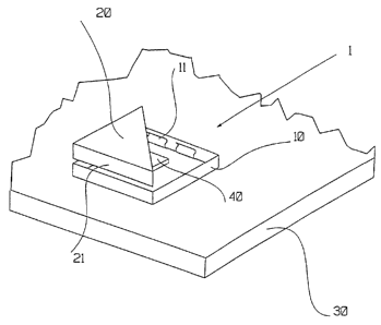
Figure 1 shows an embodiment of a protective shield of the EMC-type 1 according
to the invention. The protective shield 1 in this Figure is mounted on a substrate 30.
The protective shield comprises a frame 10 and a lid 20. The frame 10 can be fasten-
ed to the substrate 30 with the help of gluing, welding or soldering. On the inside of
the walls of the frame 10 there are a number of contact elements 1 1. These contact
elements 11 in this embodiment are shaped as tension prongs. The outer dimensions
of the lid 20 are adapted to the inner dimensions of the frame 10 according to Figure
2. When the lid 20 is forced down into the frame 10, the side walls 21 of the lid 20
are gripped between the walls of the frame 10 and the tension prongs. The compo-nent 40, which one desires to shield, is placed inside the frame 10. Said tension
prongs can also be arranged on the outside of the frame 10. The inner dimensions of
the lid 20 are in this case adapted to the shape and size of the outer dimensions of
the frame 10 so that the side walls 21 of the lid 20 are clamped between the tension
prongs and the outside of the frarne 10.
A variant for contacting the lid 20 to the frame 10 is that the outer dimension of the
frame 10 is precisely adapted to the inner dimension of the lid 20 so that these de-
tails are mechanically held together and are in electrical contact with each other by
the lid 20 being slipped over the fiame 10 and contacting it by press-fitting. It is
naturally also conceivable that the outer dimension of the lid 20 is adapted accord-
ing to the inner dimension of the frame 10 so that the lid 20 fits inside the frame 10
so that said electrical contact and mechanical holding between these parts is again
formed by press-fitting, see Figure 3.
CA 02263769 1999-02-l9
W O 98/08366 PCT/SE97/01371
s
Instead of using tension prongs or press-fitting for forrning electrical contact be-
tween the frarne 10 and the lid 20, a number of other embodiments can be conceiv-
ably used. One variant could be that the frarne 10 just like earlier is fastened to the
substrate 30 in a suitable way. ~he lid 20 is ~mensioned to either fit inside the
frame 10 or be threaded over the frame 10. If the lid 20 is intended to fit into the
frame 10, then on the outside of the side walls 21 of the lid 20 there could be
arranged a number of contact means in the shape of ribs and on the inside of theframe 10 there could be arranged corresponding ribs. The ribs of the lid 20 and the
ribs of the frame 10 snap into each other in order in this way to forrn the mechanical
and electrical contact between the lid 20 and the frame 10, see Figure 5.
Yet another variant can be that the frame 10 has a number of bulges 15 in the form
of e.g. hemispheres which are adapted to corresponding spheres on the side walls 21
of the lid. If there are a number of bulges 25 arranged on the side walls 21 of the lid
20, then there are corresponding depressions 15 arranged on the frarne 10. If on the
side walls 21 of the lid 20 there are arranged a number of depressions 25, then there
are corresponding bulges 15 arranged on the frame 10. The lid 20 can either be
adapted to be slipped over the frame 10 or to fit inside it, the depressions or bulges
25 on the side walls 21 fitting into the corresponding bulges or depressions l S on
the frame 10, see Figure 5. This embodirnent plus the one with ribs are especially
suitable in the case of small dirnensions of the protective shield.
Yet another variant for contacting the lid 20 to the frame 10 is that the lid 20 is
arranged with a number of tongues 24 along the side wall 21. These tongues 24 are
bent in towards the center of the lid 20 when the lid 20 is to be slipped over the
frame 10 and bent out from the center of the lid 20 when the lid 20 is to fit into the
frame 10, see Figure 4. The tongues can also at their free ends be bent in towards the
side wall 21.
On the frame 10 there can be arranged a flange 12 at the end which is to be cormect-
ed to the circuit board. The flange 12 can be directed in towards the center of the
CA 02263769 1999-02-19
WO 98/08366 PCT/SE97/01371
frame 10 as in Figure 3, or out from the center of the frame 10 as in Figure 4. The
flange 12 means that the frame 10 can self-adjust to the right position with the help
of the surface-tensior~ing of the f~st~nin~ material 50. If the ~ame 10 is incorrectly
placed in r~lation to a sold~ g material arranged on~}e circuit board 30, the frame
S 10 can move itself to the center of said soldering material when this begins to melt.
In order to achieve as good a shielding bandwidth as possible, the material in the
EMC-protection can be manufactured in some electrically conductive material withmagnetic qualities.
The walls of the frame 10 can be somewhat bent 12 at the bottom close to the sub-
strate 30 to which the frame 10 is fastened. The bending ofthe walls close to the
substrate can either be in towards the frame 10 or out from the same.
15 The invention is naturally not limited to the embodiments described above andshown in the drawings, but can be modified within the scope of the accompanying
claims.