Note : Les descriptions sont présentées dans la langue officielle dans laquelle elles ont été soumises.
CA 02276959 1999-07-07
1
Process for Producing Planar Waveguide Structures as well as
Waveguide Structure
The invention is based on a process for producing planar waveguide structures
as well as a
waveguide structure according to the generic class of the independent claims.
The literature, for example, "Optische Telekommunikationssysteme," [Optical
Telecommunications
Systems] Publisher Hagen Pultsch, describes manufacturing processes (see pp.
117ff.) and
waveguide structures produced by these manufacturing processes (see pp.
221ff.).
To guide light in an optical waveguide the refractive index of the waveguide
must be greater than
the refractive index of its environment. In principle, the planar waveguide
comprises a dielectric
circuit carrier, a substrate with a first refractive index n~, on which is
located a waveguiding
dielectric with a refractive index nz. The cover layer is either air or an
additional dielectric with a
refractive index n3. With this structure, light can be guided along the
boundary surfaces of the
waveguide due to repeated total reflections. Examining the field strength
distribution of a light
wave in a strip line, one can see that the field along the field boundary to
the neighboring medium
2 0 does not abruptly die down to zero. The waveguides behave as open
waveguides. If the refractive
index differences between the waveguides of the structure and the environment
are sufficiently
CA 02276959 1999-07-07
2
large, the field spurs extend only slightly out of the waveguiding structure.
To obtain optimum
waveguidance it is desirable to keep the refractive index difference large
and, in particular, to
make the structure along the boundary clean during the manufacturing process.
Various problems are encountered when manufacturing waveguide structures in
glass or silicon
material by means of known processes such as glass deposition from the vapor
phase. Under the
action of high temperatures, the waveguides are frequently deformed and are
subject to stresses.
Both problems result in poor light guidance within the waveguide. Applying an
upper cover layer
frequently causes bubble structures, which also impair the quality of the
waveguide. Furthermore,
out-diffusion of doping materials from the optical core into the surrounding
layers occurs. As a
result, the jump in the refractive index along the boundary layer is not sharp
enough to bring about
clean waveguidance.
The process according to the invention with the characteristic features of the
independent claim
has the advantage that it describes a simple way to structure the optical care
such that an optimal
symmetrical sphere surrounds the core and prevents out-diffusion of doping
materials.
Furthermore, the symmetrical sphere consisting of a fluoride-containing layer
has a stabilizing
effect on the shape of the core and thus reduces stress in the waveguide
structure.
2 0 The measures set forth in the subclaims provide an advantageous further
development and
improvement of the process defined in the independent claim.
The process is particularly advantageous for different waveguide structures
based on glass or
silicon, whereby the layers are created, for example, by flame hydrolysis. The
core structure can
advantageously be structured by a reactive ion etching process.
Furthermore, it is advantageous to produce the fluoride-containing layer by
applying a fluoride-
containing liquid. This has moreover the advantage of creating a very thin
fluoride layer, which
has a markedly changed refractive index compared to the material of the
waveguide. A layer
CA 02276959 1999-07-07
r~
3
thickness on the order of 150 nm is optimal. Applying a fluoride-containing
liquid has the additional
effect of cleaning the structure material.
The inventive waveguide with the characteristics of the independent claim has
the advantage that
it permits very clean wave guidance, whereby the manufacturing process itself
is not burdened by
costs and complex work operations.
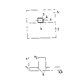
The drawing depicts an exemplary embodiment of the invention and is further
explained in the
description below. Figure 1 shows phases 1 through 4 in the production of a
waveguide, while
Figure 2 shows the index profile of a waveguide thus produced.
In a first manufacturing step, a lower layer 2, which is thick compared to the
core, is produced on
a substrate surface 1. This lower layer is made, for example, of silicon
oxide, which is doped with
boron oxide or germanium oxide. This layer is deposited on the substrate by
means of flame
hydrolysis. For this purpose, the basic substances for the process, highly
pure liquid chlorides, are
vaporized. The chlorides are introduced into the reaction chamber together
with a carrier gas and
possibly drying gases. The energy required for depositing the glass is
produced either externally
by a burner or furnace or by interaction with a plasma and high temperature.
Adding chlorides of
other elements, for example, boron or germanium, to the silicon tetrachloride
produces glasses
whose refractive index differs from that of pure quartz glass. The softening
temperature of layer 2
is highest relative to the layers subsequently to be deposited. The lower
layer 2 is sintered onto
the substrate, e.g. a silicon or quartz glass wafer. The surface of layer 2 is
etched with a fluoride-
containing solution, e.g. a BHF solution (buffered HF solution) or with
diluted hydrofluoric acid. In
the boundary phase, etching produces a thin layer with high fluoride content,
on which the
material of the next layer can subsequently be deposited. On the fluoride-
containing boundary
layer 4, a silicon oxide core layer 3 is deposited. This glass layer is doped,
for example, with
boron oxide, germanium oxide, andlor phosphorus oxide, to increase the
refractive index of the
CA 02276959 1999-07-07
x
4
glass material. Depending on the requirement of the integrated optical
structure, this layer 3
remains complete or is structured. Structuring of the waveguide can be
accomplished, for
example, by reactive ion etching (RIE). For this purpose, a plasma is produced
in the reaction
chamber, in which reactive and ionized molecules are created, which are
accelerated toward the
specimen by the voltage drop formed on the cathode, the substrate itself. This
etching process
produces, for example, the structure of waveguide 3 depicted in Figure 1.2.
CHF3 and oxygen, for
example, are used as etching gases. The entire surface structure comprising
the lower layer 2
and the waveguiding structure 3 is treated with a BHF solution or diluted
hydrofluoric acid
analogously to the process in Figure 1.1. This causes the silicate layer to be
slightly removed and
the boundary layer to be fluorinated. The fluoride-containing material has the
property of lowering
the refractive index and, what is far more interesting, of suppressing the
migration of the doping
materials within the glass the germanium, phosphorus, and boron ions [sic]. If
an optically guiding
core 3 is provided with a very thin fluoride layer 4 having an index that is
markedly changed
relative to the rest of the core material, this layer does not negatively
affect light guidance. The
preferred layer thickness is on the order of 150 nm. This layer thickness is
simultaneously
sufficient to prevent migration of the doping materials from or into the core
material. An added
effect of fluorination of the etched structure material is the cleaning of the
surface from interfering
impurities. During etching, a thin layer with high fluoride content is created
in the boundary phase
onto which the material of the core and/or the upper cover layer is
subsequently deposited. At the
2 0 same time, the fluoride-containing boundary layer has a form stabilizing
effect since the softening
point of this glass layer is higher than that of the neighboring materials.
Thus, the core is less
exposed to the pressure of the neighboring materials, the stresses are
reduced, and the refractive
index of the light guiding core remains constant due to constant concentration
and reduced
stresses. Following application of the fluoride layer in Figure 1.3, the upper
cover layer 5 is
deposited. This layer is again created by flame hydrolysis and subsequent
sintering of the
~
CA 02276959 1999-07-07
material. After completion of the production process, core 3 is uniformly sun-
ounded by a thin
fluoride layer 4. The cover layer 5 preferably has a refractive index that is
analogous to the lower
layer 2, whereby the softening temperature of the material must be lower so
that substrate, lower
layer, and core material are not excessively deformed by the sintering
process. Applying a thin
fluoride-containing layer 4 is particularly advantageous for suppressing
bubble defects caused by
sintering of cover layer 5.
Figure 2, by way of example, shows the course of the refractive index n over
cross-section axes a
and b. A strong jump in the index is evident in the region of the core
material 3. The thin fluoride-
containing layer causes a slight drop in the refractive index at the points
identified by 6. This effect
is exaggerated in the graph. It is sufficient to obtain a sharp juncture
between refractive indices n~
and n2 to describe a high-quality waveguide. Applying the fluoride-containing
layer improves the
ideally depicted jump in the refractive index to a sharper edge. Overall, this
increases the quality
of the waveguide structure and reduces optical attenuation.