Note : Les descriptions sont présentées dans la langue officielle dans laquelle elles ont été soumises.
CA 02279910 1999-08-06
WO 98/35253 PCT/GB98/00382
1
DEVICE FOR RE-DIRECTING LIGHT FROM OPTICAL WAVEGUIDE
TECHNICAL FIELD
This invention relates to a device for re-directing light from an optical
waveguide on a silicon-on-insulator chip.
BACKGROUND ART
In integrated optical circuits, there is often a requirement to re-direct
light from
an optical waveguide, e.g. from a waveguide formed on the chip to a receiver,
such as a photodiode, mounted on the chip. A variety of ways of achieving this
have been proposed in a variety of types of integrated optical circuits, e.g.
by
positioning a photodiode within a recess formed in the chip so it receives
light
emerging from a waveguide on the chip. Many of the known arrangements are.
however, difficult to fabricate accurately and inexpensively due to the
requirement of ensuring accurate positioning and alignment of the various
components concerned.
This invention aims to provide a device formed on a silicon-on-insulator chip
and which employs features of such a chip and of waveguides formed thereon
to assist in the alignment of the components of the device.
DISCLOSURE OF INVENTION
According to the present invention, there is provided a device for re-
directing
light from an optical waveguide on a silicon-on-insulator chip which comprises
a layer of silicon separated from a substrate by an insulator layer, the
device
comprising an integrated waveguide formed in the silicon layer and a
reflective
facet formed in a recess in the silicon layer, the facet being positioned to
receive light from the waveguide and angled so as to re-direct the light in a
desired direction, the waveguide and facet both being formed in the silicon
layer so their locations can be defined by the same lithographic step.
CA 02279910 1999-08-06
WO 98!35253 PCTIGB98/0a382
2
Preferred and optional features of the invention will be apparent from the
following description and from the subsidiary claims of the specification.
BRIEF DESCRIPTION OF DRAWINGS
The invention will now be further described, merely by way of example, with
reference to the accompanying drawings, in which
Figure 1 shows a schematic, perspective view of an integrated optical circuit
which includes at least one photodiode for receiving light transmitted along a
waveguide formed on the device;
Figure 2 is a schematic cross-sectional view through a silicon-on-insulator
chip
showing an embodiment of a device according to the invention for re-directing
light from a waveguide on the chip to a photodiode; and
Figures 3A to 3D show schematic plan views of various embodiments of the
device.
BEST MODE OF CARRYING OUT THE INVENTION
As indicated above, this invention relates to devices formed on silicon-on-
insulator wafers which are readily commercially available. The chip comprises
a layer of silicon separated from a silicon substrate by a layer of silicon
dioxide.
The thickness of the upper layer of silicon is typically increased to the
required
size by epitaxial growth.
Integrated optical waveguides in the form of ribs may be formed in the upper
silicon Payer. Methods of manufacturing such waveguides are described in the
paper "Low loss single mode optical waveguides with large cross-section in
silicon-on-insulator" by J. Schmidtchen et al, Electronic Letters,
27,p1486,1991.
CA 02279910 1999-08-06
WO 98135253 PCTIGB98100382
3
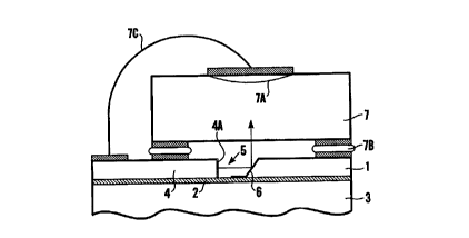
Figure 2 shows the silicon layer 1, the silicon dioxide layer 2 and the
silicon
substrate 3. A rib waveguide 4 is formed in the silicon layer 1 which is
typically
around 5 or 10 microns in thickness. The waveguide 4 terminates at a facet 4A
in a recess 5 formed in the silicon layer 1. On the opposite side of the
recess
~ 5) a facet 6 is formed on a side surtace of the silicon layer 1. The facet 6
is
coated with aluminium (or other optically reflective coating) and is angled at
54.7 degrees to the axis of the waveguide 4. Light emerging from the
waveguide facet 4A thus falls on the facet 6 and is reflected so as to be re-
directed in a direction substantially perpendicular to the plane of the chip.
With
a facet angled at 54.7 degrees to the axis of the waveguide, the light is
reflected in a direction lying 19.4 degrees to the vertical.
The facet 6 may be formed at an angle determined by a crystallographic plane
of the silicon or may be formed at other angles, e.g. by dry etching.
In another embodiment (not shown), the position of the silicon layer 1 in
which
the facet 6 is formed may have a greater thickness than the portion of the
silicon layer 1 in which the waveguide 4 is formed. The facet 6 may thus be of
larger size so a larger proportion of light diverging from the end of the
waveguide 4 is intercepted by the facet and reflected in the desired
direction.
An InGaAs photodiode 7 is soldered (7B) on the chip over the recess 5 by
standard eutectic die attach techniques so that its active region 7A is
located in
alignment with the light reflected by the angled facet 6.
Electrical connection is made to the photodiode 7 by means of a wire bond 7C
which connected with conductor tracks or circuitry provided on the upper
surface of the chip.
The arrangement described above has the benefit of being simple, yet easy to
fabricate. Alignment of the facet 6 with the waveguide 4 is achieved
CA 02279910 1999-08-06
WO 98/35253 PCT/GB98I00382
4
automatically firstly because the facet is formed in the same silicon layer in
which the waveguide is formed so is automatically aligned in the vertical
direction and, secondly, the location of the recess 5 and facet can be defined
by the same photolithographic step used to define the location of the
waveguide, so they are automatically aligned in the lateral direction.
As will be appreciated from the above, the facet is monolithically formed from
the same silicon-on-insulator chip as the silicon waveguides and, like the
waveguides, is formed in the epitaxial layer 1 of silicon rather than in the
silicon
substrate 3. The recess 5 and facet 6 are micro-machined by means of
appropriate masking and etching steps and may, for instance, be etched using
caesium hydroxide which preferentially etches the silicon layer 1. The silicon
dioxide layer 2 acts as a natural etch stop during this process.
By this means the facet 6 can be formed directly opposite the end of the
waveguide 4 and the distance between the waveguide facet 4A and the
reflective facet 6 can be kept to a minimum, e.g. to less than 15 microns, and
preferably less than 10 microns. This helps reduce losses due to the
divergence of the light emitted from the waveguide facet 4A to a minimum.
The active region 7A of the photodiode 7 typically has a diameter of around
125 microns so needs to be located on the silicon chip over the recess 5 with
a
positional tolerance of around ~ 50 microns.
It will be appreciated that a similar arrangement may be used to direct light
from a waveguide to other forms of light receivers mounted on the chip or to
direct light from a light source, e.g. a laser or light emitting diode,
mounted on
the chip into a waveguide formed thereon. A vertical cavity surface emitting
laser (not shown) may, for instance) be mounted over the recess 5 so as to
direct light onto the facet 6.
Y . . . . _.-.e.~ ~e. ....~.~. _~. _. ,
CA 02279910 1999-08-06
WO 98135253 PCT/GB98/00382
The facet 6 may be formed at other angles so as to direct light in a desired
direction. Light would typically be directed out of the plane of the chip but
may
also be directed to a device or another waveguide on the chip.
' In addition, it may be desirable to angle the facet 6 about an axis
perpendicular
to the plane of the chip to reduce problems due to back reflection,
particularly
from areas at the edge of the facet which can back-reflect into the waveguide
4
if the edges of the facet 6 lie perpendicular to the waveguide axis. A similar
result can be achieved by forming the waveguide at an angle andlor providing
an angled facet 4A on the end of the waveguide 4.
These possibilities are illustrated in Figures 3A to 3D which each show plan
views of the chip. Figure 3A shows a plan view of the arrangement illustrated
in Figure 2 which can give rise to back reflections if vertical surfaces exist
on
the facet 6. In figure 4A the light is shown being re-directed out of the
plane of
the chip in a direction normal to the chip. Figure 3B shows an arrangement in
which the facet 6 has been further tilted about an axis perpendicular to the
chip
compared to Figure 3A. Figure 3C shows an arrangement in which the
waveguide 4 is formed at an angle across the chip compared to the
arrangement of Figure 3A and Figure 3D shows an arrangement in which the
waveguide facet 4A of the waveguide 4 is angled so light emerging therefrom is
refracted away from the axis of the waveguide. In each case, the arrangement
causes the light to be re-directed out of the plane of the chip but at an
angle to
the normal thereof. This may require the position of the photodiode 7 over the
recess 5 to be adjusted slightly to ensure it receives the re-directed light.
Figure 1 shows a perspective view of an integrated optical circuit, in this
case a
transceiver, formed on a silicon-on-insulator chip 8. Two photodiodes 9 and a
laser 10 are mounted on the chip 8. Light is transmitted to the chip 8 by an
optical fibre 11 and rib waveguides 12 are provided on the chip 8 for
transmitting light to the various components. Figure 2 described above
CA 02279910 1999-08-06
WO 98135253 PCTIGB98100382
6
illustrates the manner in which light is directed from a rib waveguide 12 to
one
of the photodiodes 9.