Note : Les descriptions sont présentées dans la langue officielle dans laquelle elles ont été soumises.
CA 02284225 2002-03-O1
EIIGH POWER LASER DEVICES
S
Background of the Invention
Semiconductor lasers in common use today include edge-emitting diode lasers
and
vertical cavity surface emitting lasers (VCSELs). In an edge-emitting laser, a
semiconductor gain medium, for example a quantum-well semiconductor structure,
is
formed on a surface of a semiconductor substrate. Cavity minors are formed or
otherwise positioned on opposite sides of the substrate, perpendicular to the
substrate
surfaces, to form a resonant cavity which includes the gain medium. Electrical
or
optical pumping of the gain medium generates a laser beam whic',h propagates
in a
direction along the plane of the substrate.
Edge-emitting lasers are among the most common semiconductor laser devices.
Available commercially as individual units and in linear bar arrays, they are
used, for
example, as an optical pump source for pumping solid state lasers. High power,
typically greater than a few hundred milliwatts, adaptations of edge-emitting
lasers
commonly operate in high order spatial modes and at multiple frequencies. This
prevents their use in applications which require high power laser output in a
single
spatial mode andlor at a single frequency. Edge emitters also have a
significant degree
of astigmatism and a beam aspect ratio which is generally large, making it
difficult to
focus the beam to a small spot, which prevents their use in those applications
which
require a focused output beam. Poor beam quality in edge-emitting lasers also
makes
frequency doubling of the laser output using nonlinear optical materials
difficult and
inefficient.
CA 02284225 1999-09-20
WO 98/43329 PCT/US98/05472
-2-
In conventional VCSEL lasers, cavity mirrors are formed or otherwise
positioned
on opposite faces of a semiconductor gain medium grown on a semiconductor
substrate.
Electrical or optical pumping generates a laser beam emitted in a direction
orthogonal to
the plane of the substrate.
Conventional VCSELs find application in optical communications and optical
interconnect systems. VCSEL lasers are characterized by generally low
fundamental
spatial mode TEMP output powers, limited to about 8 milliwatts (mW) continuous
wave
(cw), and are further characterized by small fundamental spatial mode beam
diameters,
on the order of several micrometers (gym). Larger area VCSEL emitters, with
beam
diameters on the order of 100 ~m can produce output beams having a few hundred
mW
of cw output power. However, operation of conventional VCSELs at high power
and
large diameter generally carries with it the penalty of an output beam having
high-order
spatial modes and multiple frequencies. In an external cavity VCSEL
configuration,
referred to in the art as a vertical external cavity surface emitting laser
(VECSEL), an
external reflector serves as the output coupler. External cavity VECSEL
devices can
provide higher fundamental spatial mode output power than VCSEL devices.
Previous work on external cavity vertically emitting semiconductor lasers
typically resulted in low output power. The work of Sandusky and Brueck, for
example,
produced low output power and used optical pumping to excite the
semiconductor. See
J. V. Sandusky and S. R. J. Brueck, "A cw external cavity surface-emitting
laser",
nics Technology Letters, vol. 8 pp. 313-315, 1996. In a study by Hadley et
al., an
electrically excited VCSEL in an external cavity produced 2.4 mW cw and 100 mW
pulsed in a fundamental spatial mode. In this case, an emitting area up to 120
~cm was
used. See M. A. Hadley, G. C. Wilson, K. Y. Lau and J. S. Smith, "High single-
traverse mode output from external cavity surface emitting laser diodes",
Applied Phys.
Letters, vol. 63, pp. 1607-1609, 1993.
For various laser applications, a beam generated by the laser is subjected to
frequency conversion or frequency doubling. This is accomplished by
introducing a
non-linear material, for example KTP, KTN, KNb03, and LiNh03 into the laser
path.
The frequency of a beam incident on the non-linear material is converted to a
second
frequency. The non-linear materials are referred to as "doubling crystals"
where the
CA 02284225 1999-09-20
WO 98/43329 PCT/US98/OS472
-3-
property of the material is such that it serves to double the frequency of a
beam
traversing the crystal. Efficient frequency conversion by the material
generally requires
a high-intensity, single mode incident beam.
Frequency doubling of semiconductor lasers has been demonstrated in the past
to
varying degrees of success using a doubling crystal mounted external to an
edge-emitting
diode laser cavity. The output beams from edge-emitting diode lasers are
usually highly
divergent and have significant aspect ratios as well as some degree of
astigmatism which
degrades the optical field intensity and phase front from that which is
ideally required for
efficient frequency doubling. Experiments have been carried out in which the
light from
a diode laser is launched into an optical waveguide fabricated in a non-linear
material in
order to maintain the optical field intensity over some relatively long path
length. This
technique is generally complicated and uses relatively low power diode lasers
which have
sufficient beam quality to launch the laser light into the external waveguide.
Various techniques in the past have attempted to harness beam power to enable
efficient conversion. A first technique by Gunter, P. Gunter et al. "Nonlinear
optical
crystals for optical frequency doubling with laser diodes", Proc. of SPIE,
vol. 236,
pages 8-18, 1980, demonstrated low efficiency frequency doubling of diode
laser
radiation using potassium niobate KNb03 in a single-pass doubling
configuration. In
another technique, Koslovsky et al., Optics Letters 12, 1014, 1987, employed a
single
spatial mode, edge-emitting diode laser and KNbO~ in an external ring
resonator to
increase the circulating power to achieve frequency conversion. The Koslovsky
configuration required frequency-locking of the single-frequency laser to the
Fabry-Perot
resonance of the ring cavity as well as matching the temperature of the non-
linear crystal
to both frequencies. This required complicated crystal alignment and
wavelength control
circuitry to maintain frequency locking.
Summar~of the Invention
The present invention is directed to an apparatus and method for generating
high
power laser radiation in a single fundamental spatial mode, in a manner which
overcomes the aforementioned limitations. The laser of the present invention,
when
configured in an external cavity, is especially amenable to frequency
conversion of the
__ CA 02284225 1999-09-20
WO 98/43329 PCTNS98/05472
-4-
output beam, as it provides beam power densities over suitable path lengths
for efficient
frequency conversion.
In a first embodiment of the present invention, the apparatus comprises a
resonant
cavity defined between first and second partial reflectors. The geometry of
the resonant
cavity defines a fundamental spatial or transverse cavity mode. A gain medium
is
disposed within the resonant cavity, and an energy source energizes the gain
medium
within a first volume. This causes spontaneous and stimulated energy emission
to
propagate in the gain medium in a direction transverse to the fundamental
cavity mode.
The transverse emission, in turn, optically pumps a second volume of the gain
medium
about the first volume. When the intensity of the spontaneous emission is
sufficiently
high, inversion and gain are produced in the second volume. The energy within
the first
and second volumes is coupled into the fundamental cavity mode laser beam.
By optimizing the geometry of the cavity such that the fundamental cavity mode
is coupled to both the first and second volumes, the energy of the first
volume
transversely-directed into the second volume, which would otherwise be wasted,
is
instead captured by the fundamental beam, improving the overall power
efficiency of the
laser. To effect this, in a preferred embodiment, the cavity mirrors are
selected to match
the fundamental cavity mode to the cross-sectional diameter of the second
volume. In
this manner, the laser energy in the fundamental spatial mode is efficiently
extracted
from both first and second volumes of the gain medium. Similar results apply
where the
output energy is in a higher order spatial mode.
In a preferred embodiment, the first volume is substantially cylindrical and
of
cross sectional diameter D,, and the second volume is substantially an annulus
of outer
cross-sectional diameter D~ and inner cross-sectional diameter D, , the first
and second
volumes being substantially cross-sectionally concentric.
The gain medium is preferably formed of a semiconductor material in a vertical
cavity configuration. Alternatively, the gain medium may be formed of a solid
state
material having an active ion which has absorption in the spectral region of
the gain
transition. Examples of such solid state materials include Er:glass, Yb:glass,
and
Yb:YAG. In the case of solid state materials, pump energy would be preferably
generated by optical means, for example a diode laser.
CA 02284225 1999-09-20
WO 98/43329 PCT/US98/05472
-5-
A nonlinear crystal may be placed in the optical cavity or external to the
laser to
change the laser output frequency. Suitable materials for nonlinear conversion
include
KTP, KTN, KNb03, and LiNb03 and periodically-poled materials such as
periodically-
. poled LiNb03.
A preferred embodiment of the present invention, described in detail below, is
capable of generating intracavity circulating power levels in excess of 100 kW
in a
fundamental spatial mode for a 1 mm diameter beam. These levels are sufficient
for
producing harmonic conversion of the fundamental radiation in a non-linear
material. As
an example, frequency doubling in a semiconductor configuration using GaInAs
gain
media provides a fundamental wavelength of 900 nm to 1100 nm and a frequency
doubled output in the blue to green wavelengths.
Brief Description of the Drawings
The foregoing and other objects, features and advantages of the invention will
be
apparent from the more particular description of preferred embodiments of the
invention,
as illustrated in the accompanying drawings in which like reference characters
refer to
the same parts throughout the different views. The drawings are not
necessarily to scale,
emphasis instead being placed upon illustrating the principles of the
invention.
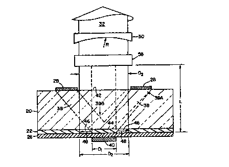
FIG. 1 is a perspective view of a VECSEL laser configuration in accordance
with
the present invention.
FIG. 2 is a cutaway side view of the configuration of FIG. 1 illustrating
transverse propagation of spontaneous and stimulated emission from the first
pumped
volume into the second annular volume in accordance with the present
invention.
FIG. 3 is a perspective view of a VCSEL laser configuration illustrating the
relationship of the first pumped volume and the second annular volume in
accordance
with the present invention.
FIG. 4 is a perspective illustration of an optical amplifier configuration in
accordance with the present invention.
FIG. 5 is a side view of a coupling configuration for coupling output energy
into
a fiber-optic.
CA 02284225 2002-03-O1
WO 98/43329 PCTIUS98105472
-6-
Detailed Description of Preferred Embodiments
FIG. 1 is a perspective view of a preferred embodiment of the present
invention,
in a VECSEL configuration. The laser of FIG. I includes a semiconductor
substrate 20,
upon a first face of which is formed a semiconductor quantum-yell gain region
22. A
S first reflector 26, for example a p-Bragg reflector, is formed on the
quantum-well region
22. A second external reflector 30 is positioned opposite the first reflector
26. The
distance between the first and second reflectors 26, 30 and their respective
curvatures
define a fundamental cavity mode in a resonant cavity 60. The second reflector
30 is
illustrated as an external cavity mirror in FIG. I in accordance with a VECSEL
config-
uration; however, the second reflector 30 may alternatively be layered
directly adjacent
the second face of the substrate to provide a VCSEL configuration.. Note that
for
purposes of the present invention, the term "reflector" as used herc;in
includes partially
andlor fully reflective materials andlor surfaces. The surface 42 of the
substrate 20
facing the second reflector 30 preferably is treated with an anti-reflection
coating 42,
such that any beam energy in the resonant cavity 60 traversing that; interface
will pass
with minimal reflection, a desirable feature as is well known in the; prior
art.
As shown in the cross-sectional illustration of FIG. 2, the resonant cavity is
pumped electrically through an annular electrical contact 28, causing current
38 to flow
between annular contact 28 and circular contact 40 on opposite faces of the
substrate 20.
The resulting current flow 38 is generally conical in shape, the base 39A of
the cone
being at the annular contact 28 and the peak of the cone 39B being near
contact 40. The
flow in the peak 39B is generally circular in cross section and energizes a
first
substantially cylindrical volume 44 of the gain region 22, the first volume 44
being of a
cross-sectional diameter D,. The diameter D, is preferably substantially
greater than the
thickness of the gain region 22.
The excited gain region 22 of diameter D, generates stimulated and spontaneous
emission, represented by arrows 48, which travels in a direction transverse to
the
propagation of the cavity laser beam. In standard prior-art VCSEL or VECSEL
lasers,
such energy would escape out the sides of the device or would otherwise be
wasted as
energy not contributing to the output beam 32. In the configuration of the
present
invention, this transverse energy 48 is absorbed in a second annular volume 46
CA 02284225 1999-09-20
WO 98/43329 PCT/US98/05472
_7_
surrounding the first pumped volume. This absorbed energy serves to pump the
second
volume 46, providing gain and therefore power into the fundamental laser mode
60.
When the electrical or optical pumping of the first region D, produces gain,
this
gain occurs for both the transverse and longitudinal directions. Since the
traverse gain
S length is larger than the longitudinal gain length, more stimulated emission
can occur in
that direction. The larger the dimension D,, the greater the net gain for
stimulated
emission in the transverse direction. Higher output power requires larger area
devices
because of thermal dissipation and the limit set by catastrophic degradation
by the optical
power density on the surface of the semiconductor in the longitudinal
direction. For
such large area devices, significant power can be lost by the occurrence of
the transverse
stimulated emission thereby reducing the overall power conversion efficiency.
Spontaneous emission also occurs but becomes less important for the larger
area devices.
If the adjacent region is designed to absorb the stimulated emission (and also
to a lesser
extent the spontaneous emission), then the energy that otherwise would have
been lost
can be used to optically pump the second region D2 to the extent that it will
produce
gain. The energy pumped into the second region DZ can be extracted in the
orthogonal
direction by adjusting the external minor 30 to produce a mode waist equal to
DZ on the
gain medium. The external cavity mirror 30 will fix or "clamp" the gain in the
total area
defined by D, and D2. There is a limit to the extent of the second region DZ,
as the
degree of transverse pumping decreases with decreasing intensity away from the
center
of the pumped region. This limit is related to the dimension D, and the
pumping
intensity (electrical or optical) in the area defined by D,
Given the mode waist diameter D2, the technique for designing a cavity which
would provide a suitable radius of curvature R for the second reflector 30 and
the
suitable optical cavity length L is well known in the art. See, for example,
Herwig
Kogelnik and Tingye Lee, "Beams, Modes, and Resonators" , CRC Handbook of
Lasers,
CRC Press, 1971, pg. 421-441. The second diameter DZ is a function of the
excitation
level and the diameter D,. The design would be optimized for maximum output
power
limited by the circulating power density, which is limited by catastrophic
degradation of
the semiconductor, and the thermal power dissipation from the second diameter
D2. The
CA 02284225 2002-03-O1
WO 98/43329 PCT/US98/OS472
l!
mode waist diameter for the cavity could be matched, for example, by adjusting
the
cavity length L for a fixed radius of curvature R for the second reflector 30.
FIG. 3 is a perspective view of a laser in a VSCEL configuration in accordance
f
with the present invention illustrating the relationship of the first pumped
volume 44 and
the second output volume 46. The pumped first volume 44 is of diameter Di in
the
region of the gain medium 22. The transverse propagation of spontaneous arid
stimulated emission represented by arrows 48 optically pumps or otherwise
energizes an
annular volume 46 surrounding the first volume 44.
The annular volume 46 has an inner diameter of D, and an outer diameter of D~
and is
substantially cross-sectionaliy concentric with the first volume 44 assuming a
Gaussian
beam distribution. The fundamental cavity mode is optimized to have a diameter
approximately equal to the outer diameter D, of the second volume 46, such
that energy
in both first and second volumes is captured and therefore contributes to the
output beam
32. Excitation of the first volume 44, may occur by electrical or optical
means.
The laser cavity parameters are preferably adjusted to set the mode waist
substantially equal to the diameter D~ at the maximum operating power levels.
In a laser
cavity comprising a single flat mirror 26 and a single concave spherical
mirror 30 having
a radius of curvature R as shown in FIG. 2, the mode beam diameter on the
laser chip w,
and at the output mirror w, is characterized by:
w,2 = 4~,L/n[(R - L)/L]'~ (1)
w22 = 4~.R,/~[L/(R - L)]'h (2)
where L is the cavity length and ~, is the wavelength of the output laser beam
32 as
described in Kogelnik et al. cited above. It is clear from these equations
that the
diameter of the fundamental laser mode can be made equal to the outer diameter
D~ of
the second volume 46, for example by adjusting the cavity length L for a
specific radius
of curvature R. Alternatively, the radius of curvature R may be selected for a
specific
range of cavity lengths L. Instead of curved mirrors, a flat output coupler 30
may be
CA 02284225 2002-03-O1
w0 98/43329 PCT/US98/05472
-9-
employed with a lens in the cavity, of appropriate geometry to achieve the
same results.
A physical lens or thermal lens may be used for this purpose.
A preferred embodiment of a semiconductor laser device ;may comprise a
multiple element quantum well structure or a single gain region having a total
gain
thickness equivalent to that of a multiple quantum well structure. In order to
achieve
sufficient single pass gain, a 900 nanometer (nm) to 1100 nm wavelength laser
structure
formed in a semiconductor material such as GaInAs preferably has at least five
quantum
wells or an equivalent thickness. For more efficient operation, at least ten
quantum
wells are used in order to effectively overcome the optical losses due to free
carrier
absorption at the laser wavelength in the conductive substrate layer 20. A
typical
thickness for a single quantum well is approximately 8 nrn. Note that the
optical
bandgap is dependent on the thickness of the quantum well and therefore an
equivalent
thickness for a single layer of gain material would have its wavelength
somewhat shifted
from the same compositional structure for the narrow quantum well material.
'The total
thickness or the number of quantum wells can be increased to increase the gain
to
overcome all intracavity losses for efficient operation. This is limited only
by the ability
to unifornily grow such structures arrd by the practical threshold current
density for such
structures. Conventional VCSEL.s typically operate with only one or a few
quantum
wells between very high reflectivity mirrors. Such devices exhibit low optical
gain and
therefore would not operate as efficiently as the apparatus of the present
invention.
The electrical current or optical pump energy injected into the laser device
can be
provided by any of the well-known methods, for example in G.F'. Agarwal,
"Semiconductor Lasers", The American Institute of Physics Pre:;s, pages 146-
157. In a
preferred embodiment of the present invention, most of the injection current
38 is
directed into a circular region of a diameter equal to or less than the
diameter D, of the
fundamental spatial mode as defined by equations ( 1 ) and (2) above.
As described above, low efficiency frequency doubling of diode laser radiation
using edge-emitting diode lasers has been demonstrated in the past by Gunter
and
Koslovsky et al. In contrast, the preferred embodiment of the present
invention employs
a VCSEL or VECSEL vertical cavity laser structure in which the total single
pass gain is
significantly lower than in edge-emitting lasers. In addition, the output from
the vertical
CA 02284225 1999-09-20
WO 98/43329 PCT/US98105472
-10-
cavity device of the present invention is distributed over a much larger
circular beam
area than in edge-emitting devices, for example several hundred times greater
in area.
The achievable intracavity circulating power density in a fundamental circular
spatial
mode can exceed several MW/cm2, limited only by catastrophic degradation at
the
semiconductor surface. While similar power densities can be achieved in edge-
emitting
lasers, the beam is confined to the waveguide of the diode cavity which makes
frequency
doubling difficult. Since the efficiency of frequency conversion is dependent
on both
the optical intensity and the length of the interaction region, frequency
doubling of diode
lasers is complicated and has been carried out in waveguide structures to
maintain the
field intensity of a sufficient interaction distance. A high conversion
efficiency can be
achieved in the present invention since high optical field intensities can be
maintained
over a sufficiently long interaction length because the beam is substantially
non-divergent
within the optical laser cavity. A high quality beam provides a more favorable
frequency
conversion situation for any conversion configuration outside of the cavity
such as in the
recently-studied periodically-poled nonlinear materials. Furthermore, the
present
invention can be operated in a pulsed, gain-switched, or mode-locked
configuration to
increase the optical power and therefore the nonlinear conversion efficiency.
The
present invention applies not only to harmonic frequency conversion, but also
to sum and
difference frequency generation. In a preferred embodiment, the non-linear
material
includes Fabry-Perot resonances such that the laser operates in a single
frequency. An
exemplary configuration is illustrated in FIG. 2, which includes an
intracavity non-linear
crystal 58 between the substrate 20 and external mirror 30.
Each prior art configuration mentioned above, for example the Sandusky et al.
and Hadley et al. configuration, was limited by matching the cavity geometry
to the
extent of the pumped volume only, unlike the present invention which extracts
energy
from the first pumped volume in addition to the second volume energized by
transverse
energy emission generated in the first volume.
The output power in the present invention can be magnified by increasing the
diameter of the mode volume, as described above. Peak output power levels, for
example in excess of 10 kW, can be generated from a gain area of one
millimeter in
CA 02284225 1999-09-20
WO 98/43329 PCT/US98/05472
-11-
diameter. Continuous cw output power levels may exceed 10 Watts from a single
element device, limited only by thermal considerations.
A second harmonic radiation which propagates in the backward direction can
additionally be absorbed in a semiconductor laser structure in such a way as
to produce
electrons and holes which migrate to the active gain region, thereby
increasing the power
of the fundamental laser radiation. This also has the effect of increasing
efficiency of the
second harmonic output as well as producing a single-ended output of harmonic
radiation. In an alternative embodiment, a three-mirror cavity could be used
in which
the nonlinear material is disposed in a position in which the harmonic
radiation does not
reflect back into the gain medium but exits through the middle mirror. A ring
resonator
configuration may also be employed.
Typical frequency doubling materials appropriate for conversion of infrared
wavelengths into the visible include periodically-poled LiNb03, KTP, and
KNb03. For
example KTP can be phase matched to convert 1 ~,m radiation into green
wavelengths
and KNb03 can convert infrared radiation into blue wavelengths using GaInAs
diode
lasers operating in the 900 nm wavelength range.
Many configurations for intracavity frequency doubling that are well known in
the field can be used in the present invention. For example, a focusing lens
can be
positioned within the laser resonator defined by the mirrors 24 and 30 to
increase the
power density. The technique would allow use of very short lengths of
nonlinear
materials or nonlinear materials with lower nonlinear figures-of merit.
For doubling materials such as KTP and KNb03, active crystal lengths can be
significantly less than I cm for the circulating power levels possible in the
present
configurations. Shorter nonlinear material lengths provide wider temperature
and
wavelength phase matching conditions. For KNbOj for example, a crystal length
of 1
mm or less can provide a temperature phase matching bandwidth of more than
several
degrees Celsius and a wavelength bandwidth of several nanometers. Such broad
acceptance ranges make the manufacture and operation of such devices
significantly
more practical. The wavelength may be controlled by the selection of the alloy
composition of the gain medium material, while precision wavelength control is
CA 02284225 2002-03-O1
WO 98/43329 PCT/US98/05472
-I2-
achievable with intracavity etalons or other wavelength controlling
tecturiques well
known in the art. Similar results apply to other non-linear rnat<:rials,
including KTP.
The semiconductor gain region 22 preferably comprises a multiple-element
quantum
well structure. Alternatively, a single gain region whose total lain thickness
is equal to
S that of the multiple quantum well structure may be employed. In order to
achieve
sufficient single pass gain, the number of quantum wells typical, for a 900 nm
to 1100 nm
wavelength laser structure made from GaInAs should be more than 5 with a
typical range
of between 10 and 25 wells. For a high-peak-power device operating under
pulsed
conditions using either electrical or optical excitation, the number of wells
may be more
than 50. The limit is governed by the practical ability to grow large numbers
of strain-
free quantum well layers. In this case, a heterostructure may be a more
effective choice.
high-peak-power devices could be made, for example, by using high-power Q-
switched
solid state lasers as pump sources.
Conventional vertical cavity semiconductor lasers typically operate with only
one or
a few quaruum wells and very high reflectivity cavity mirrors. Such devices
may not
operate as efficiently in tl7e prcaenc invention because of inherently low
optical gain.
The net gain must be sufficient to overcome losses in the external cavity
including the
free carrier loss in the substrate material 22 and the optical losses in the
nonlinear
material and associated anti-reflection coating on the intracavity optical
elements.
FIG. 2 illustrates a typical quantum-well device 22 formed on a semiconductor
substrate 20. A highly reflective mirror 26 is grown on the back surface of
the device to
provide one of the mirrors of the laser resonator. The top cladding layer
serves as a
conductive contact which can be antireflection coated 42 and which has low
optical
absorption at the laser wavelength. In an alternative embodiment, a layer of
electrically-
conductive material with an optical bandgap greater than the second harmonic
radiation
serves as the conductive layer with a second layer, of thickness less than the
diffusion
length of carriers and transparent to the fundamental laser radiation, and
absorbing the
second harmonic radiation grown between the active material a.nd the thick
wide-bandgap
material, would allow the optically excited carriers to diffuse into the gain
region. The
thick conductive material may comprise for example, deposited tin oxide.
- CA 02284225 1999-09-20
WO 98/43329 PCTlUS98/05472
-13-
Single frequency operation may be achieved, for example, by introducing an
etalon
in the cavity. Alternatively, the non-linear crystal 58 may also serve as a
frequency
selective element.
The ability to generate visible wavelengths in high-power output makes the
present
invention attractive to a range of applications including projection display,
optical disc
read and write, optical holographic memory storage, and bio-fluorescence
sensors. For
the case of projection display, three primary colors could be generated. For
example,
the blue wavelength and green wavelength could be produced by frequency
doubling the
output of GaInAs semiconductor lasers whose outputs could be selected in the
wavelength range from 900 nm to more than 1100 nm. Appropriate frequency
doubling
materials include KTP for the green wavelength and KNbO; for the blue
wavelength.
Power may be scaled using arrays of such devices. Output power levels of
several tens
of Watts may be generated. Since the output from such an array would lack
coherence
between elements of the array, the effects of speckle would be significantly
reduced so as
not to affect the quality of the projected image in the display system. In the
case of an
array device, the output couplers may comprise an array of lithographically-
produced
binary optical mirrors or micromirrors whose positions are precisely aligned
with the
center of the diode laser emitting areas.
A projection display system employing the present invention could be operated
using
various light valve devices such as liquid crystal spatial light modulators,
micro-mirrors
such as those sold by Texas Instruments, and grating deflector light valves
such as those
developed by Silicon Light Machines of Sunnyvale, California. For an array of
laser
sources, all elements of the light valve could be illuminated by every laser
source by
allowing the individual laser beams to expand so they overlap in the far
field. In this
way, the failure of one element would not significantly degrade the operation
of the
system. Binary optical lenses may be used to focus the laser light in a top-
hat
distribution onto each pixel of the light valve to make efficient use of all
available laser
radiation.
While this invention has been particularly shown and described with references
to
preferred embodiments thereof, it will be understood by those skilled in the
art that
CA 02284225 1999-09-20
WO 98/43329 PCTNS98/05472
-14-
various changes in form and details may be made therein without departing from
the
spirit and scope of the invention as defined by the appended claims.
As an example of an alternative embodiment, FIG. 4 is a perspective
illustration of
the present invention configured as an optical amplifier 70. As in the laser
configuration, the optical amplifier 70 configuration includes a semiconductor
substrate
20, a semiconductor gain medium 22, and a first reflector 26. Note that a
second
reflector is not required as the optical amplifier 70 does not include a
resonant cavity. A
first volume 44 of the gain medium 22 is pumped with electrical or optical
energy 56.
The first volume 44 is generally cross-sectionally circular, having a diameter
D,. As
described above, this causes transverse stimulated and spontaneous propagation
of
energy 48 into a second volume 46 about the first volume 44. In a preferred
embodiment, the second volume 46 is substantially circular in cross-section,
the diameter
being DZ. An incident beam 50 of diameter DZ and of a first amplitude is
directed at the
pumped region 46, overlapping with and being energized by both the first
volume 44
and second volume 46. The incident beam 50 reflects at minor 26 and is
released as an
output beam 52 of similar diameter DZ. The output beam 52 is amplified by the
energized gain region 46 and is therefore of higher intensity than the
incident beam S0.
A plurality of such gain elements may be used to increase the total gain of
the system.
A second alternative embodiment is illustrated in FIG. 5, representative of a
side
view of an optical coupling configuration. A single mirror/lens element 70
includes a
first concave face 72 which operates as a resonator mirror for VECSEL laser
78, and a
second convex face 74 which operates as a focusing element for directing laser
radiation
32 into fiber-optic 76. The fiber-optic 76 may comprise single-mode or multi-
mode
fiber, and is positioned at the focus of the laser radiation 32 such that the
laser energy is
directed substantially within the numerical aperture of the fiber. The
reflectivity of the
first surface 72 is optimized to maximize output power from the laser device
78, while
the second surface 74 and the input surface 75 of fiber optic 76 are anti-
reflection coated
at the laser wavelength to minimize reflectivity.
CA 02284225 1999-09-20
WO 98/43329 PCT/US98/05472
-I5-
During assembly, the mirror/lens element 70 is aligned and positioned to
maximize laser output power coupling, and is fixed using well-known
techniques,
including soldering, epoxying and/or laser welding. The fiber is then
positioned to
accept the focused radiation 32 and is set accordingly by any of the above
techniques.
This embodiment offers the advantage of a reduction of the number of optical
elements
required to focus energy into a fiber by incorporating the function of a
cavity mirror and
an output lens into a single element.