Note : Les descriptions sont présentées dans la langue officielle dans laquelle elles ont été soumises.
CA 02285341 1999-09-29
SPECIFICATION
IMAGE SENSOR CHIP AND
IMAGE READING APPARATUS INCORPORATING THE SAME
FIELD OF THE INVENTION
The present invention relates to an image sensor chip for
use as a component of an image reading apparatus. It also
relates to an image reading apparatus employing such an image
sensor chip.
BACKGROUNG OF THE INVENTION
An image sensor chip is known which is elongated in a
direction and which has a surface portion integrally
incorporating a plurality of light receiving elements for
photoelectric conversion. Each of the light receiving
elements has a light receiving surface for receiving light and
for generating an image signal with an output level
corresponding to the received amount of light. The respective
light receiving surfaces serve as the picture elements of the
image sensor chip and are arranged in a row at a constant pitch
longitudinally of the image sensor chip.
The length of such an image sensor chip ranges from several
millimeters to less than 20 millimeters, so that a single image
sensor chip fails to read a document which is wider than it.
Therefore, in actual use of the image sensor chip as a component
of an image reading apparatus, a plurality of such image sensor
chips are arranged in an array.
1
CA 02285341 1999-09-29
When using a plurality of image sensor chips in this way,
they may suffer fluctuations in the output level of their image
signals due to manufacturing errors of the image sensor chips
and positional deviations relative to the lens of the image
reading apparatus even if the light receiving elements receive
an equal amount of light. Accordingly, image reading is
performed by a plurality of image sensor chips, the image
signals outputted from the plurality of light receiving
elements are subjected to level correction to prevent
unevenness in the output level. In this regard, if the level
correction is performed individually for all signals from the
light receiving elements, the process will be very cumbersome.
Therefore, as a simple way to perform the level correction,
the correction is performed collectively for each group of e.g.
eight light receiving elements, wherein the image signal
outputted from one of the eight light receiving elements in
the group is used as the basis for the correction.
On the other hand, the number of the light receiving elements
incorporated in a prior art image sensor chip is, for example,
32, 64 or 128 which is an integer multiple of 16. This is
convenient for the above-described level correction because
the light receiving elements of the image sensor chip can be
exactly divided into plural groups of eight elements without
any excess.
However, the prior art image sensor chip still has the
following problems:
For image reading of a document by using an array of image
sensor chips, the image sensor chip array is required to provide
an image reading width (substantially equal to the combined
2
CA 02285341 1999-09-29
length of the image sensor chips in the array) which is greater
by an suitable excess than the document width. If the image
reading width is excessively greater than the document width,
the image sensor chips may be partially wasted, and the image
reading apparatusbecomesunnecessarilylarge. Conversely, if
the excess of the image reading width is too small, the image
sensor chip array may fails to read a side part of the document
even due to a slight deviation of the document positioning.
Here, in order for the above-described excess to be suitable,
it should be relatively smaller for a narrower document but
relatively larger for a wider document. This is because, in
reading a narrow document accurately, the document is unlikely
to positionally deviate too much in the primary scanning
direction (or in the direction of the row of the image reading
picture elements), whereas, in reading a wide document, the
document is likely to positionally deviate in the primary
scanning direction to a large extent.
However, the prior art image sensor chip is incapable of
meeting the requirements . Taking an image sensor chip of 10 . 84
mm in length with a resolution of 11.8 dots/mm as an example,
it has 128 image reading picture elements . In order for such
an image sensor chip to meet a variety of reading width
requirements, the specifications shown in Table 1 below are
called for.
(Continued to Page 4)
3
CA 02285341 1999-09-29
Table 1
Required ReadingNumber of Chip Array Excess Lb Excess Ratio
Width S (mm) Required Length La (mm) R
Chips (mm) (%)
25.4 ( 1 inch 3 32.52 7.12 28.05
)
50.8 ( 2 inch 5 54.21 3.41 6.71
)
76.2 ( 3 inch 8 86.73 10.53 13.82
)
101.6 ( 4 inch10 108.42 6.82 6.71
)
127 ( 5 inch 12 130.10 3.10 2.44
)
152.4 ( 6 inch14 162.62 10.22 6.71
)
177.8 ( 7 inch17 184.31 6.51 3.66
)
203.2 ( 8 inch19 205.99 2.79 1.37
)
215.9 ( 8.5 20 216.83 0.93 0.43
inch )
254 ( 10 inch 24 260.20 6.20 2.44
)
Taking an image sensor chip of 8 mm in length with a
resolution of 8 dots/mm as another example, it has 64 image
reading picture elements. In order for such an image sensor
chip to meet various reading width requirements, the
specifications shown in Table 2 below are called for.
(Continued to Page 5)
4
CA 02285341 1999-09-29
Table 2
Required ReadingNumber of Chip Array Excess Lb Excess Ratio
Width S (mm) Required Length La (mm) R
Chips (mm) (%)
25.4 ( 1 inch 4 32.00 6.60 25.98
)
50.8 ( 2 inch 7 56.00 5.20 10.24
)
76.2 ( 3 inch 10 80.00 3.80 4.99
)
101.6 ( 4 inch13 104.00 2.40 2.36
)
127 ( 5 inch 16 128.00 1.00 0.79
)
152.4 ( 6 inch20 160.00 7.60 4.99
)
177.8 ( 7 inch23 184.00 6.20 3.49
)
203.2 ( 8 inch26 208.00 4.80 2.36
)
215.9 ( 8.5 27 216.00 0.10 0.05
inch )
254 ( 10 inch 32 256.00 2.00 0.79
)
As appreciated from Tables 1 and 2, when using a given number
of conventional image sensor chips in an array for meeting the
required reading width S, the excess Lb of the chip array length
which is the difference between the required reading width S
and the chip array length La becomes smaller as the required
reading width S increases. Similarly, the excess ratio
(R=Lb/S) also becomes gradually smaller. In this way, the use
of the conventional image sensor chips directly contradicts
the above-mentioned requirements, making it difficult to
suitably adjust the excess Lb to the required reading width
S. As a result, if an attempt is made to use a minimum number
of conventional image ser_sor chips for saving, even a slight
deviation of the document may cause difficulty in performing
5
CA 02285341 1999-09-29
appropriate image reading due to an unduly small excess Lb.
Further, the use of an excessive number of image sensor chips
for overcoming such a problem will result in added cost while
causing a size increase of the image reading apparatus as a
whole.
SUMMARY OF THE INVENTION
It is therefore an object of the present invention to provide
an image sensor chip which is capable of eliminating or
alleviating the problems described above.
It is another object of the present invention to provide
an image reading apparatus employing such a image sensor chip .
According to a first aspect of the present invention, there
is provided an image sensor chip comprising: a plurality of
light receiving elements for photoelectric conversion, the
plurality of light receiving elements having light receiving
surfaces serving as a plurality of image reading picture
elements, the plurality of image reading picture elements being
arranged in a row at a constant pitch on the chip; wherein the
number N of the image reading picture elements is defined as
N=n~k (other than an integer multiple of 16); wherein n
represents the number of image signals processed as a group
when the image signals from the light receiving elements are
subjected to level correction on a group-by-group basis;
wherein k is a minimum integer satisfying 0<(n-k- y ~p)<n;
wherein y is a resolution defined as the number of image reading
picture elements per predetermined unit length; and wherein
p is a minimum difference between required reading widths as
calculated on the basis of said unit length.
6
CA 02285341 1999-09-29
Preferably, the chip comprises a semiconductor chip which
has a rectangular shape elongated in a direction, and the
plurality of light receiving elements are built in the chip
as arranged in said direction.
Preferably, the image sensor chip further comprises a
built-in circuit for operating the plurality of light receiving
elements.
Preferably, n is 8, y is 11.8 dots/mm, and the number N
of the reading picture elements is 152.
Preferably, n is 8, y is 8 dots/mm, and the number N of
the image reading picture elements is 104.
According to a second aspect of the present invention, there
is provided an image reading apparatus comprising: a plurality
of image sensor chips carrying a plurality of light receiving
elements for photoelectric conversion, the plurality of light
receiving elements having light receiving surfaces serving as
a plurality of image reading picture elements, the plurality
of image reading picture elements being arranged in a row at
a constant pitch on the chip; a substrate carrying thereon the
plurality of image sensor chips arranged in an array; a light
source for irradiating a reading line area of a document image
with light; a lens for focusing the light, which is irradiated
by the light source and reflected from the document, at the
plurality of image reading picture elements; wherein the number
N of the image reading picture elements is defined as N=n~k
(other than an integer multiple of 16); wherein n represents
the number of image signals processed as a group when the image
signals from the light receiving elements are subjected to level
correction on a group-by-group basis; wherein k is a minimum
7
CA 02285341 1999-09-29
integer satisfying 0<(n~k-y~p)<n; wherein y is a resolution
defined as the number of image reading picture elements per
predetermined unit length; wherein p is a minimum difference
between required reading widths as calculated on the basis of
said unit length.
As the number N of the image reading picture elements
satisfies the condition described above, the present invention
has following advantages.
Firstly, when arranging a plurality of image sensor chips
in an array for providing any one of the required reading widths
which is an integer multiple of p, it is only necessary to use
only a minimum number of image sensor chips whichever reading
width is selected, whereby the excess of the image sensor chip
array relative to the actual reading width can be kept at a
constant ratio relative to the selected reading width.
Therefore, the present invention allows the excess of the image
sensor chip array to be smaller for a narrower document but
larger for a wider document. Consequently, according to the
present-invention as opposed to the prior art, when using a
plurality of image sensor chips in an array for providing a
desired reading width, it is possible to reduce a waste with
respect to the number and length of the image sensor chips,
thereby reducing the cost while realizing a size reduction of
the image reading apparatus incorporating such image sensor
chips. Further, since the reading width of the image sensor
chip array still has a reasonable excess, it is possible to
avoid an image reading difficulty which may be caused due to
a positional deviation of the document deviation.
8
CA 02285341 1999-09-29
Secondly, the number N of the image reading picture elements
is an integer multiple of the number of the image signals
processed together in a single group for group-by-group level
correction, the plurality of image signals outputted from each
image sensor chip can be divided into a plurality of groups
without any remainder for the level correction. Therefore,
according to the present invention, the plurality of image
signals outputted separately from two image sensor chips need
not be grouped together for correction even though the plurality
of image sensor chips are arranged in an array. Thus, it is
possible to avoid the disadvantage previously encountered with
the prior in level correction.
Other features and advantages of the present invention will
become apparent from the detailed description given below with
reference to the accompanying drawings.
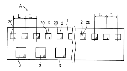
Fig. 1 is a plan view of an image sensor chip embodying the
present invention.
Fig. 2 is a circuit block diagram schematically
illustrating a circuit arrangement of the image sensor chip
shown in Fig. 1.
Fig. 3 is a schematic plan view showing a circuit board which
is provided with the image sensor chip shown in Fig. 1.
Fig. 4 is a schematic sectional view showing an example of
image reading apparatus employing the image sensor chip shown
in Fig. 1.
9
CA 02285341 1999-09-29
DETAILED DESCRIPTION OF THE PREFERRED EMBODIMENT
The preferred embodiment of the present invention will be
specifically described below with reference to the accompanying
drawings.
Fig . 1 shows an image sensor chip A which is an elongated
rectangular semiconductor chip. The chip includes, for
example, a thin silicon substrate 1 formed integrally with an
N number (described hereinafter) of light receiving elements
2 and a circuit for operating the light receiving elements 2.
Each of the light receiving elements 2 comprises a
phototransistor for photoelectric conversion and has a
rectangular or square light receiving surface 20, respectively.
The light receiving surfaces 20 serve as image reading picture
elements as arranged in a row at a constant pitch L
longitudinally of the substrate 1 over the entire length thereof .
The surface of the image sensor chip A is covered with an
insulating protective coating (not shown). However, the
protective coating has a plurality of windows corresponding
in size and arrangement to the light receiving surfaces 20.
Each of the light receiving surfaces 20 receives light through
the respective window. The surface of the protective coating
is provided a plurality of pads 3 for electrically connecting
the built-in circuit of the image sensor chip A with the
exterior.
Fig. 2 illustrates a circuit arrangement of the image sensor
chip A. The image sensor chip A comprises phototransistors Tr
providing an N number of light receiving elements 2, an FET
connected to the emitter of each phototransistor Tr, an
amplifier OP for amplifying the current from the respective
CA 02285341 1999-09-29
EFT, a N-bit shift register 19, a pad VDD, a pad GND, a pad
A0, a pad SI, a pad CLK, and a pad S0. These pads are divisionally
located at a plurality of pad arranging portions 3. The pad
VDD is provided with a power supply of 5 volts for example.
The pad GND is connected to a grounding line . The pad CLK is
fed with clock signals of e. g. 8 MHz . The pad SI receives serial
input signals. The pad AO provides serial output of analog
image signals each corresponding to the amount of light received
by the respective phototransistor Tr. The pad SO provides
serial output signals.
With such a circuit arrangement, when serial-in signals are
supplied to the pad SI, the shift register 19 turns on the N
number of FETs successively. Then, the electrical charge
stored in the N number of phototransistors Tr is released
successively for serial output through the pad AO after
amplification at the amplifier OP. When the image signal from
the final Nth phototransistor Tr is outputted by operation of
the shift register 19, a serial-out signal is supplied through
the pad S0. The image sensor chip A is designed to repeat such
a series of operations.
Next, description is made with respect to the number N of
the image reading picture elements of the image sensor chip
A.
The number N of the image reading picture elements is def fined
as N=n~k, where the n represents the number of the image signals
processed in a group when the image signals from the light
receiving elements 2 are subjected to level correction on a
group-by-group basis . The value of the n is "8" for example,
as is conventionally the case.
11
CA 02285341 1999-09-29
The k is a minimum integer satisfying 0< (n~k- y ~p) <n. The
y is a resolution defined as the number of image reading picture
elements per predetermined unit length. If the pitch L between
the light receiving surfaces is approximately 0.085 mm for
example, the resolution y is 11.8 dots/mm. If an inch is taken
as a unit length, the resolution y is 300 dpi (dpi being the
abbreviation for dot/inch). The p is the minimum difference
between required reading widths. Specifically, the minimum
difference p is the value which is determined according to the
customer's requests or the type of the image reader made by
the manufacturer. Where a plurality of image sensor chips A
are used to provide various reading widths, the smallest one
of the differences between the various reading widths is the
minimum difference referred to here. For example, as shown in
Table 3 below, if the image sensor chips A are required to provide
the reading widths S of 25.4 mm (1 inch), 50.8 mm (2 inch),
76.2 mm (3 inch) ~~~ 203.2 mm (8 inch) , 215.9 mm(8.5 inch) , 254
mm (10 inch) , the minimum difference p is 12.7 mm (1/2 inch) .
This minimum difference p is, however, calculated on the basis
of the unit length (1 inch) used for the resolution y , i.e.,
1/2 inches in this case.
Under the above condition, y ~p=300X (1/2)=150. The value
of y ~p corresponds to the number of the image reading picture
elements needed for reading the minimum difference p between
the required reading widths . The value of the k as the minimum
integer satisfying 0<(n~k-y~p)<n is k=19 for n=8 and D=150.
Accordingly, the substitution of 19 for k in N=n~k described
above gives N=152. Thus, 152 light receiving elements 2 are
integrated in the image sensor chip A, or the number N of the
12
CA 02285341 1999-09-29
image reading picture elements is 152 . As a result, the length
of the image sensor chip A is approximately 12.874 mm.
Next, description is made as to the use and advantages of
the image sensor chip A.
As shown in Fig. 3, a plurality of image sensor chips A are
prepared and mounted in an array on a surface of a circuit board
4. The surface of the circuit board 4 is formed with a wiring
pattern (not shown) for electrically connecting to the pads
3 of the plural image sensor chips A. The pads 3 of the plural
image sensor chips A are connected to the wiring pattern via
gold wires (not shown) in a manner such that the plural image
sensor chips A are electrically connected to each other in
series . On the other hand, the number of the image sensor chips
A mounted on the circuit board 4 is optionally selected
according to the reading width required for a target image
reader to which the image sensors are incorporated. The
concrete specifications are given in Table 3.
(Continued to Page 14)
13
CA 02285341 1999-09-29
Table 3
Required ReadingNumber of Chip Array Excess Lb Excess Ratio
Width S (mm) Required Length La (mm) R
Chips (mm) (%)
25.4 ( 1 inch2 25.75 0.35 1.37
)
50.8 ( 2 inch4 51.50 0.70 1.37
)
76.2 ( 3 inch6 77.25 1.05 1.37
)
101.6 ( 4 8 103.00 1.40 1.37
inch )
127 ( 5 inch 10 128.74 1.74 1.37
)
152.4 ( 6 12 154.49 2.09 1.37
inch )
177.8 ( 7 14 180.24 2.44 1.37
inch )
203.2 ( 8 16 205.99 2.79 1.37
inch )
215.9 ( 8.5 17 218.86 2.96 1.37
inch )
254 ( 10 inch20 257.49 3.49 1.37
)
As appreciated from Table 3 , for a required reading width
S of 25.4 mm (1 inch) for example, only two image sensor chips
are needed, thereby providing an array length La of
approximately 25.75 mm for the two image sensor chips A. An
excess Lb of the image sensor chip array length La over the
required reading width S is approximately 0.35 mm, resulting
in an excess ratio R of approximately 1 . 37~ . By contrast, as
the required reading width S increases to 50.8 mm and 76.2 mm,
respectively, by increments of 25.4 mm (1 inch), the excess
Lb of the image sensor chip array length La over the required
reading width S also increases gradually, but the excess ratio
R still remains at approximately 1.37 as in the case for the
required reading width S of 25.4 mm. Further, even if the
14
CA 02285341 1999-09-29
required reading width S changes by increments of 12.7 mm (1/2
inch) to e.g. 215.9 mm, the excess ratio R still remains at
approximately 1.37.
As described above, when a plurality of image sensor chips
A are used for meeting the requirement of reading width S, it
is possible to always keep the excess ratio R constant for any
required width S by using only a minimum number of image sensor
chips A needed for exceeding the required reading width S.
Accordingly, wasteful use of image sensor chips Amaybe avoided.
Given a constant excess ratio R, the excess Lb is smaller for
a smaller required reading width S, consequently reducing the
useless area in the array of the image sensor chips A.
Conversely, the excess Lb is larger for a lager reading width
S, so that the whole image on the document can be scanned
appropriately even if the document to be read positionally
deviates slightly in the primary scanning direction.
As opposed to the above example of conditions, if the
resolution y is changed to 203 dpi (8 dots/mm) for example with
the values of n and p maintained n=8 and p=1/2 inch (12.7 mm) ,
respectively, the number N of the image reading picture elements
in the image sensor chip A is calculated as N=8 X 13=104 because
of y -p=101.5 and k=13. In this case, the length of a single
chip is l3.mm. The specifications for such image sensor chips
to meet various reading width requirements is given in Table
4 below.
(Continued to Page 16)
CA 02285341 1999-09-29
Table 4
Required ReadingNumber of Chip Array Excess Lb Excess Ratio
Width S (mm) Required Length La (mm) R
Chips (mm) (%)
25.4 ( 1 inch2 26.00 0.60 2.36
)
50.8 ( 2 inch4 52.00 1.20 2.36
)
76.2 ( 3 inch6 78.00 1.80 2.36
)
101.6 ( 4 8 104.00 2.40 2.36
inch )
127 ( 5 inch 10 130.00 3.00 2.36
)
152.4 ( 6 12 156.00 3.60 2.36
inch )
177.8 ( 7 14 182.00 4.20 2.36
inch )
203.2 ( 8 16 208.00 4.80 2.36
inch )
215.9 ( 8.5 17 221.00 5.10 2.36
inch )
254 ( 10 inch20 260.00 6.00 2.36
)
As appreciated from Table 4, the ratio R of the excess Lb
of the image sensor chip array can also be maintained at a
constant value of approximately 2.36 if the required reading
width S is an integer multiple of the minimum difference p (p=1/2
inch) between the required different readinct widths.
Therefore, the excess Lb is smaller for a smaller required
reading width S but becomes gradually larger as the required
reading width S increases.
Next, description is made with respect to the structure of
an image reading apparatus employing such image sensor chips
A.
Fig. 4 shows an image reading apparatus B which is basically
identical in structure to a known image reader. The image
16
CA 02285341 1999-09-29
reader B includes a case 50 provided with a transparent board
51. A predetermined line area on a surface of the transparent
board 51 serves as an image reading area 52. A platen roller
6 is provided in opposite to the image reading area 52 for
transferring a document 59 in the secondary scanning direction.
The case 50 is internally provided with a light source 53 such
as LEDs for irradiating the image reading area 52 with light,
and a lens 54 is disposed right below the image reading area
52 for condensing the light . The lens 54 may comprise an array
of self-focusing lens for forming a non-inverted, non-magnified
image of the document. A circuit board 4 carrying a plurality
of image sensor chips A is mounted at the bottom of the case
50 with the image sensor chips A positioned right below the
lens 54.
With the image reader B described above, the light from the
light source 53 reaches the image reading area 52 to irradiate
the surface of the document 59. Then, the light reflected from
the document is focused at the light receiving surface 20 of
each image sensor chip A for serial output of an image signal
with an output level corresponding to the amount of light
received at the respective light receiving surface 20.
As previously described, the use of the above-described
image sensor chips A in the image reader B can avoid using too
many image sensor chips A. Accordingly, the length of the
circuit board 4 can be shortened while also realizing the size
reduction of other components such as the lens 54, the case
50 and so on. Consequently, the image reader B may be downsized,
and the manufacturing cost may be reduced.
17
CA 02285341 1999-09-29
Every 8 signals of the image signals from the light receiving
elements grouped together for level correction or output level
adjustment . On the other hand, the number N of the image reading
picture elements in each image sensor chip A is, for example,
152 or 104 which is an integer multiple of 8. Therefore, the
level correction can be performed appropriately for each image
sensor chip A on a chip-by-chip basis. More specifically, when
the number N of the image reading picture elements is 152 , the
152 image signals from the single image sensor chip A are divided
exactly into 19 groups, so that there is no need for performing
the correction process over two image sensor chips. If, for
example, the image signals outputted separately from the two
image sensor chips A are grouped together for level correction,
manufacturing fluctuations between the two image sensor chips
and/or a difference in position relative to the lens 54 may
result in inappropriate level correction. Therefore, the
level correction of the image signals should be preferably
performed within every image sensor chip. The above-described
design meets such a requirement appropriately.
The specific design of the image sensor chip and the image
reading apparatus according to the present invention should
not be limited to the above-described embodiment but may be
modified variously.
For instance, in accordance with the present invention, the
specific values for y , n and p may differ from those previously
described.
Further, the resolution y and the minimum difference p
between the required different reading widths need not be
expressed in inches. According to the present invention, when
18
CA 02285341 1999-09-29
the required reading widths changes at an interval of 50 mm
like 100 mm, 150 mm and 200 mm, this length of 50 mm may be
used as an unit length for the resolution y and the minimum
difference p. In this case, the number of the image reading
picture elements per 50 mm may be used as the resolution y,
and if the minimum difference p between the required reading
widths is 50 mm, this minimum difference p may treated as a
unity.
Since the number of the image reading picture elements in
a conventional image sensor chip is an integer multiple of 16,
the number N of the image reading picture elements according
to the present invention excludes multiples of 16.
19