Sélection de la langue

Search

Sommaire du brevet 2292907 

Énoncé de désistement de responsabilité concernant l'information provenant de tiers

Une partie des informations de ce site Web a été fournie par des sources externes. Le gouvernement du Canada n'assume aucune responsabilité concernant la précision, l'actualité ou la fiabilité des informations fournies par les sources externes. Les utilisateurs qui désirent employer cette information devraient consulter directement la source des informations. Le contenu fourni par les sources externes n'est pas assujetti aux exigences sur les langues officielles, la protection des renseignements personnels et l'accessibilité.

Disponibilité de l'Abrégé et des Revendications

L'apparition de différences dans le texte et l'image des Revendications et de l'Abrégé dépend du moment auquel le document est publié. Les textes des Revendications et de l'Abrégé sont affichés :

  • lorsque la demande peut être examinée par le public;
  • lorsque le brevet est émis (délivrance).
(12) Brevet: (11) CA 2292907
(54) Titre français: GUIDE D'ONDES
(54) Titre anglais: WAVEGUIDE
Statut: Réputé périmé
Données bibliographiques
(51) Classification internationale des brevets (CIB):
  • H01S 5/10 (2006.01)
  • G02B 6/12 (2006.01)
  • G02B 6/122 (2006.01)
  • H01S 5/026 (2006.01)
(72) Inventeurs :
  • WEBER, JEAN-PIERRE (DECEASED) (Suède)
(73) Titulaires :
  • TELEFONAKTIEBOLAGET LM ERICSSON (Suède)
(71) Demandeurs :
  • TELEFONAKTIEBOLAGET LM ERICSSON (Suède)
(74) Agent: ERICSSON CANADA PATENT GROUP
(74) Co-agent:
(45) Délivré: 2005-08-09
(86) Date de dépôt PCT: 1998-06-02
(87) Mise à la disponibilité du public: 1998-12-10
Requête d'examen: 2003-06-02
Licence disponible: S.O.
(25) Langue des documents déposés: Anglais

Traité de coopération en matière de brevets (PCT): Oui
(86) Numéro de la demande PCT: PCT/EP1998/003300
(87) Numéro de publication internationale PCT: WO1998/056085
(85) Entrée nationale: 1999-12-03

(30) Données de priorité de la demande:
Numéro de la demande Pays / territoire Date
9711835.0 Royaume-Uni 1997-06-06

Abrégés

Abrégé français

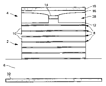
L'invention concerne un laser à semi-conducteur pouvant être couplé bout à bout avec une fibre optique, grâce au fait qu'à une zone d'extrémité du laser, une puissance est couplée, à partir d'un guide d'ondes actif à mode étroit, dans un guide d'ondes passif à mode large. Le guide d'ondes actif présente une conicité asymétrique formée par attaque chimique diagonale à travers la couche active lors de la fabrication.


Abrégé anglais


The invention relates to a semiconductor laser, which can be butt-joint
coupled to an optical fibre, by virtue of the fact that, in an
end region of the laser device, power is coupled from an active waveguide,
with a narrow mode, into a passive waveguide, with a wide
mode. The active waveguide has an asymmetrical taper, formed by a diagonal
etch across the active layer during fabrication.

Revendications

Note : Les revendications sont présentées dans la langue officielle dans laquelle elles ont été soumises.


-7-

CLAIMS

1. A method of fabricating a semiconductor
device, comprising:
forming a passive waveguide from a plurality of
alternating layers of passive guide material and
cladding material on a substrate;
forming an active region on the passive waveguide;
etching the material of the active region to form
a diagonal end face thereof in a first end region of
the device;
regrowing semi-insulating material to replace the
material removed by etching the material of the active
region;
etching the material of the active region and the
regrown semi-insulating material to define an active
waveguide;
growing current blocking layers to replace the
material removed by etching the material of the active
region and the regrown semi-insulating material; and
etching all the regrown material down to the
substrate to define a ridge waveguide in the said first
end region.
2. A semiconductor optical device, comprising a
first passive waveguide and a second active waveguide,
the second waveguide being tapered in the region of an
end of the device, characterized in that the width
of the second waveguide is tapered asymmetrically.
3. A semiconductor optical device as claimed in
claim 2, characterised in that the passive waveguide is
in the form of a ridge waveguide at the end of the
device.

Description

Note : Les descriptions sont présentées dans la langue officielle dans laquelle elles ont été soumises.


CA 02292907 1999-12-03
WO 98156085 PCT/EP98/03300
WAVEGUIDE
BACKGROUND OF THE INVENTION
- The present invention relates to a semiconductor
optical device, such as a laser, and to a method of
fabrication thereof, which allows low-loss coupling to
an optical fibre.
DESCRIPTION OF THE PRIOR ART
Semiconductor optical components, such as
semiconductor lasers, are widely used. In use, it is
often necessary to couple such components to external
optical elements. For example, in the case of a
semiconductor laser producing a coherent light output,
it may be necessary to couple the device to an optical
fibre, along which the light is to be directed.
One problem which arises with such coupling is
that there can be high losses (up to 10 dB), arising
from the different optical modes which exist in the
laser and in the fibre. Typically, the optical fibre
has a circularly symmetric mode, with a Full Width
Half-Max (FWHM) of the order of 7~,m, while the mode in
the laser is usually elliptical, with the ratio of the
major axis to the minor axis being about 2:1, and with
the FWHM being about l~,m.
One solution to this problem is to use lenses, but
this is expensive, and is not usually practical if it
is desired to make an array of lasers. Ideally, it
should be possible simply to place the er:3 of the fibre
against the output face of the laser, and join them
using butt-joint coupling.
If this is to be possible, the mode size at the
output of the laser mu~~ be increased, so that it is a
better match to the mode within the fibre. Or~4 such
proposal is disclosed in United States Patent No.
5,278,926. In this document, it is proposed that the
semiconductor optical component should include two
buried heterostructure optical waveguides, namely an
SUBSTITUTE SHEET (RULE 26)


CA 02292907 1999-12-03
WO 98156085 PCT/EP98/03300
-2-
active waveguide and a passive waveguide which are
superposed over at least a part of their lengths, the
transverse cross-sectional area of the active waveguide
decreasing over a mode transition region to couple a
narrow optical mode, which is guided by the active
waveguide, to a wide mode, which is guided by the
passive waveguide.
One object of the present invention is to provide
a fabrication process which allows relatively easy
manufacture of an optical component such as a laser,
which may be coupled to an optical fibre.
A further object of the invention is to define a
structure which allows easy coupling to an optical
fibre.
The present invention relates to a method of
fabricating the semiconductor laser which allows the
use of standard fabrication techniques, without
requiring particularly tight manufacturing tolerances.
Moreover, the invention relates to the structure made
by this fabrication process. In particular, there is
also disclosed a structure with ar. asymmetrically
tapered waveguide.
rRIEF DESCRIPTION OF THE DRAWINGS
Figure 1 is a cross-sectional view through a
component in accordance with the invention.
Figure 2 is a plan view of the component shown in
Figure 1.
Figure 3 is a plan view of the component during
fabrication.
Figure 4 is a plan view of the component at a
later point during fabrication.
DETAILED DESCRIPTION OF THE PREFERRED EMBODIMENTS
Figures 1 and 2 are, respectively, a cross-
sectional view and a plan view of a semiconductor laser
component in accordance with the invention. A process
for fabricating the device will now be described. This
SUBSTITUTE SHEET (RULE 26)


CA 02292907 1999-12-03
WO 98/56085 PCT/EP98/03300
-3-
will be with reference to a laser at 1.55~em, having a
bulk active layer. It will be appreciated that the
active layer could also be formed of quantum wells or
strained quantum wells. All of the materials are
lattice-matched. In the following description, all of
the growth steps are advantageously carried out using
Metal Organic Chemical Vapour Deposition (MOCVD),
although it will be appreciated that other growth
techniques may be used.
The first stage in the fabrication process is
epitaxial growth of the layers which form the passive
waveguide 2 and the active waveguide 4. In this
example, the substrate 5 is n-doped InP, and the
passive waveguide 2, which is also n-doped, is formed
on the substrate in a number of layers. Each layer
comprises passive waveguide material 8, in the form of
a 40nm layer of InGaAsP with a l.OUm band gap, and
cladding material 10, in the form of a 660nm layer of
:LnP. Figure 1 shows a passive waveguide having seven
such layers, but the number of layers may be eight, or
nine, or indeed any convenient number.
On top of the uppermost layer of passive waveguide
material 8, there is grown a 460nm layer of n-doped InP
12, followed by the active layer 14, which is formed
from 0.2~Cm undoped InGaAsP, witm 1.58~m band gap. A
further cladding layer 16, formed from p-doped InP and
of thickness of about 200nm is then grown on the active
layer.
The next stage in the fabrication process involves
the formation of an asymmetric taper in the active
waveguide 4, in the second region 22 shown in Figure 2.
This taper. is formed by etching diagonally through the
active layer. In the finished product, the taper, and
hence the second region 22, might for example extend
over a length in the region from 50~m to several
hundred ~cm. This means that the diagonal etch must be
SUBSTITUTE SHEET (RULE 26)


CA 02292907 1999-12-03
WO 98/56085 PCT/EP98/03300
-4-
at an angle of about 0.003-0.03 radians to the
waveguide direction. The etch is through the active
layer 14, down to the uppermost n-InP layer.
Then, selective regrowth with semi-insulating (Fe-
doped) InP is used to form current blocking layers 28
to fill the etched regions and planarise the wafer.
Alternatively, n-P InP can be used for the current
blocking layers.
Figure 3 is a plan view of the device at this
stage, showing the diagonal etch through the active
guide layer 4, and the regrowth of semi-insulating InP
30. (The angle of the diagonal etch is greatly
exaggerated in Figure 3 for ease of illustration).
The next fabrication stage is the formation of a
standard buried heterostructure layer, that is the
formation of the active waveguide itself, with a width
of about l.2um by etching through the active layer,
down into the uppermost n-InP layer. It will be noted
that this also extends into the region which was etched
and refilled with semi-insulating InP in the previous
stage. The reason for regrowing the semi-insulating
material was to obtain a planar surface for easy
lithography while defining the active waveguide. The
result is that an asymmetric taper can be obtained
without having to form sharp points by lithography, and
without constructing any free-standing thin points at
any stage during processing, as these are susceptible
to breakage.
Figure 4 is a plan view of the device following
the definition of the active waveguide. At this stage,
it is possible to see the active waveguide 4, the
regrown semi-insulating material 30, and the passive
waveguide 2 in the areas where the active layer has
been etched away.
Following definition of the active waveguide, a
standard current blocking structure 28 is formed from
SUBSTITUTE SHEET (RULE 26)


CA 02292907 1999-12-03
WO 98/56085 PCT/EP98/03300
_5_
p-n InP, or from semi-insulating (Fe doped) InP.
To complete the buried heterostructure layer, a p-
InP cladding 16 is grown over the whole structure, and
a p-InGaAs layer 18 is formed to provide good ohmic
contact to the top metal layer which acts as the
contact.
The next step is the definition of a large ridge
waveguide around the region where the active layer has
been etched away (including the taper region), as shown
in Figures 1 and 2. The waveguide is of the order of
ll~m wide, centred on the active waveguide, and is
defined by etching away all the regrown material down
to the substrate.
A bottom contact 32 is formed by metallisation of
the substrate surface. The laser facets can then be
formed by cleaving or etching, and can eventually be
coated. The whole structure may be covered by SiN,
although the performance is the same if air is used as
the outer dielectric material.
This structure can be used for a Fabry-Perot
laser, in which case mirrors are provided on the end
facets of the cavity, which may be cleaved or etched
and may be coated or uncoated. Alternatively, the
structure may be used for a DFB laser, although, in
this case, additional steps are required before
formation of the contact layer 18 to make the required
gratings, and an anti-reflect; on coating is then
applied to the facets.
As mentioned previously, Figure 2 is a plan view
of the semiconductor laser device in accordance with
the invention. The device can be considered to be
divided into three regions. In a first region 20, the
device has a normal laser structure, though with a
passive waveguide 2 and an active waveguide 4. In this
region, nearly all of the power is confined to the
active waveguide 4. In a second region 22, the active
SUBSTITUTE SHEET (RULE 26)


CA 02292907 1999-12-03
WO 98/56085 PCT/EP98/03300
-6-
waveguide is tapered down to zero, which leads to an
adiabatic transfer of the power from the active guide
to the passive guide 2. Finally, in the third region
24, the power is confined to the large passive guide,
which has a mode which can be well matched to an
optical fibre 26, to which the laser is to be coupled.
In the first region 20 of the device, the ridge is
not etched, in order to avoid formation of another
guided mode. However, in the second and third regions,
i.e. at the output side of the laser, the ridge
waveguide is formed by etching through the whole
structure, down to the substrate, to define the large
passive ridge waveguide, which preferably has a width
of about ll~.m. It should be noted that neither the
width of the ridge waveguide, nor indeed the width of
the active region, are critical, which allows good
manufacturing tolerances. The thickness of the layers,
which are also not critical, can be controlled much
more accurately than the widths of the layers.
SUBSTITUTE SHEET (RULE 26)

Dessin représentatif
Une figure unique qui représente un dessin illustrant l'invention.
États administratifs

Pour une meilleure compréhension de l'état de la demande ou brevet qui figure sur cette page, la rubrique Mise en garde , et les descriptions de Brevet , États administratifs , Taxes périodiques et Historique des paiements devraient être consultées.

États administratifs

Titre Date
Date de délivrance prévu 2005-08-09
(86) Date de dépôt PCT 1998-06-02
(87) Date de publication PCT 1998-12-10
(85) Entrée nationale 1999-12-03
Requête d'examen 2003-06-02
(45) Délivré 2005-08-09
Réputé périmé 2017-06-02

Historique d'abandonnement

Il n'y a pas d'historique d'abandonnement

Historique des paiements

Type de taxes Anniversaire Échéance Montant payé Date payée
Le dépôt d'une demande de brevet 300,00 $ 1999-12-03
Taxe de maintien en état - Demande - nouvelle loi 2 2000-06-02 100,00 $ 2000-05-25
Enregistrement de documents 100,00 $ 2000-10-20
Taxe de maintien en état - Demande - nouvelle loi 3 2001-06-04 100,00 $ 2001-05-24
Taxe de maintien en état - Demande - nouvelle loi 4 2002-06-03 100,00 $ 2002-05-28
Taxe de maintien en état - Demande - nouvelle loi 5 2003-06-02 150,00 $ 2003-05-30
Requête d'examen 400,00 $ 2003-06-02
Taxe de maintien en état - Demande - nouvelle loi 6 2004-06-02 200,00 $ 2004-10-15
Expiré 2019 - Taxe de paiement en souffrance, selon le par. 3.1(1) 2004-11-28 50,00 $ 2004-10-15
Taxe finale 300,00 $ 2005-04-01
Taxe de maintien en état - Demande - nouvelle loi 7 2005-06-02 200,00 $ 2005-05-24
Taxe de maintien en état - brevet - nouvelle loi 8 2006-06-02 200,00 $ 2006-05-25
Taxe de maintien en état - brevet - nouvelle loi 9 2007-06-04 200,00 $ 2007-05-24
Taxe de maintien en état - brevet - nouvelle loi 10 2008-06-02 250,00 $ 2008-05-23
Taxe de maintien en état - brevet - nouvelle loi 11 2009-06-02 250,00 $ 2009-05-28
Taxe de maintien en état - brevet - nouvelle loi 12 2010-06-02 250,00 $ 2010-05-25
Taxe de maintien en état - brevet - nouvelle loi 13 2011-06-02 250,00 $ 2011-05-30
Taxe de maintien en état - brevet - nouvelle loi 14 2012-06-04 250,00 $ 2012-05-24
Taxe de maintien en état - brevet - nouvelle loi 15 2013-06-03 450,00 $ 2013-05-24
Taxe de maintien en état - brevet - nouvelle loi 16 2014-06-02 450,00 $ 2014-05-27
Taxe de maintien en état - brevet - nouvelle loi 17 2015-06-02 450,00 $ 2015-05-25
Titulaires au dossier

Les titulaires actuels et antérieures au dossier sont affichés en ordre alphabétique.

Titulaires actuels au dossier
TELEFONAKTIEBOLAGET LM ERICSSON
Titulaires antérieures au dossier
WEBER, JEAN-PIERRE (DECEASED)
Les propriétaires antérieurs qui ne figurent pas dans la liste des « Propriétaires au dossier » apparaîtront dans d'autres documents au dossier.
Documents

Pour visionner les fichiers sélectionnés, entrer le code reCAPTCHA :


Pour visualiser une image, cliquer sur un lien dans la colonne description du document. Pour télécharger l'image (les images), cliquer l'une ou plusieurs cases à cocher dans la première colonne et ensuite cliquer sur le bouton "Télécharger sélection en format PDF (archive Zip)" ou le bouton "Télécharger sélection (en un fichier PDF fusionné)".

Liste des documents de brevet publiés et non publiés sur la BDBC .

Si vous avez des difficultés à accéder au contenu, veuillez communiquer avec le Centre de services à la clientèle au 1-866-997-1936, ou envoyer un courriel au Centre de service à la clientèle de l'OPIC.


Description du
Document 
Date
(yyyy-mm-dd) 
Nombre de pages   Taille de l'image (Ko) 
Dessins 1999-12-03 2 30
Dessins représentatifs 2000-02-14 1 4
Abrégé 1999-12-03 1 46
Description 1999-12-03 6 264
Revendications 1999-12-03 1 37
Page couverture 2000-02-14 1 31
Dessins représentatifs 2004-10-28 1 16
Page couverture 2005-07-28 1 43
Poursuite-Amendment 2003-06-02 1 29
Correspondance 2000-01-20 1 2
Cession 1999-12-03 2 88
PCT 1999-12-03 12 370
Cession 2000-10-20 6 338
Correspondance 2003-10-31 8 381
Correspondance 2003-11-14 1 13
Correspondance 2003-11-18 1 26
Taxes 2004-09-28 1 25
Correspondance 2005-04-01 1 25