Note : Les descriptions sont présentées dans la langue officielle dans laquelle elles ont été soumises.
_.
CA 02297255 2000-O1-21
WO 99105893 PCTlUS98/12321
ELECTRONIC BALLAST SYSTEM
This invention pertains generally to fluorescent lighting and, more
particularly,
to an electronic ballast system for fluorescent lamps.
Heretofore, electronic ballasts have been provided for use with fluorescent
lamps. Examples of such ballasts are found in U.S. Patents 4,245,178 and
4,631,449.
Electronic ballasts typically operate at frequencies on the order of 10 KHz to
100 KHz, and are designed to provide high circuit efficiency, high
reliability,
and low cost. While the physical size and weight of ballasts are dependent
upon operating frequency, with higher frequencies permitting ballasts to be
smaller in size and lighter in weight, reductions in size and weight have not
been easy to achieve.
In order to reduce losses, multiple wires or Litz wires have been used for
transformer windings, but they add substantially to the cost of manufacture.
The cost can be reduced somewhat by using single conductor, continuous
windings on power transformers. However, that substantially reduces the
coefficient of coupling and can result in high leakage flux which puts a heavy
stress both on the transformer itself and on any switching devices or diodes
'used in the high energy path. In addition, leakage flux can also produce high
voltage spikes and can cause electromagnetic interference in the nearby
environment.
CA 02297255 2000-O1-21
WO 99105893
PCT/US98112321
_2_ _-
The higher flux drives and higher circulating currents required for reactive
loading of a power transformer in prior systems can also increase core loss
as well as loss in the windings themselves. To avoid such losses, it has
heretofore been necessary to use larger cores and multiple conductors in the
transformer windings.
It is in general an object of the invention to provide a new and improved
ballast system for fluorescent lights.
Another object of the invention is to provide a ballast system of the above
character which overcomes the limitations and disadvantages of the prior art.
These and other objects are achieved in accordance with the invention by
providing an electronic ballast system which has a transformer with primary
and secondary windings, a power oscillator connected to the primary winding
for operation at a predetermined frequency in the range of 10 KHz to 5 MHz,
and a ballasting network connected to the secondary winding and adapted for
connection to the fluorescent lamp, with the ballasting network being resonant
at a frequency within about t10 percent of the predetermined frequency when
connected to the lamp. In some embodiments, the resonant frequency of the
ballasting network remains the same regardless of the number of lamps
connected to it. Due to the resonance in the ballasting network, only
resistive
loading transformation occurs in the power transformer.
Figure 1 is a circuit diagram of one embodiment of an electronic ballast
system according to the invention.
Figure 2 is an AC equivalent circuit of the primary section of the system of
Figure 1.
Figure 3 is a set of waveform diagrams of the voltages at certain points in
the
system of Figure 1.
CA 02297255 2000-O1-21
WO 99105893 PCT/US98112321
_3. _-
Figures 4 - 7 are circuit diagrams of other embodiments of ballasting networks
for use in the system of Figure 1.
Figures 8 - 9 are circuit diagrams of additional embodiments of an electronic
ballast system according to the invention.
Figure 10 is an AC equivalent circuit of the primary section of the embodiment
of Figure 9.
Figures 11 - 13 are circuit diagrams of additional embodiments of an
electronic ballast system according to the invention.
Figures 14a and 14b are AC equivalent circuits of the primary section of the
embodiment of Figure 13.
Figure 15 is a set of waveform diagrams of the voltages at certain points in
the embodiment of Figure 13.
Figure 16 is a circuit diagram of another embodiment of an electronic ballast
system according to the invention.
i 5 Figures 17a and 17b are AC equivalent circuits of the primary section of
the
embodiment of Figure 16.
Figure 18 is a circuit diagram of another embodiment of an electronic ballast
system according to the invention.
Figures 19a and 19b are AC equivalent circuits of the primary section of the
embodiment of Figure 18.
Figure 20 is a set of waveform diagrams of the voltages at certain points in
the embodiment of Figure 18.
CA 02297255 2000-O1-21
WO 99/05893 PCTIUS98/12321
_4_ __
Figures 21 and 22 are circuit diagrams of additional embodiments of an
electronic ballast system according to the invention.
Figure 23 is a circuit diagram of another embodiment of an electronic ballast
system according to the invention.
Figures 24a and 24b are AC equivalent circuits of the primary section of the
embodiment of Figure 23.
Figure 25 is a set of waveform diagrams of the voltages at certain points in
the embodiment of Figure 23.
Figure 26 is a circuit diagram of another embodiment of an electronic ballast
system according to the invention.
Figures 27a and 27b are AC equivalent circuits of the primary section of the
embodiment of Figure 18.
Figure 28 is a circuit diagram of another embodiment of an electronic ballast
system according to the invention.
Figure 29 is a set of waveform diagrams of the voltages and currents at
certain points in the embodiment of Figure 28.
Figure 30 is a circuit diagram of another embodiment of an electronic ballast
system according to the invention.
Figure 31 is a cross-sectional view, somewhat schematic, of one embodiment
of a transformer for use in the ballast system of the preceding figures.
Figure 32 is a cross-sectional view taken along line 32-32 of Figure 31, with
a portion of the core structure removed for clarity of illustration.
CA 02297255 2000-O1-21
WO 99/05893 PCTIUS98112321
_5_ _-
Figure 33 is a cross-sectional view of another embodiment of a shield for use
in the transformer of Figure 31.
Figures 34 and 35 are isometric views of additional embodiments of
transformers for use in the ballast system of Figures 1 - 30.
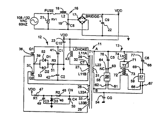
As illustrated in Figure 1, the ballast system includes a transformer 11, a
power oscillator 12 connected to the primary of the transformer, and a
ballasting network 13 connected to the secondary of the transformer. As
discussed hereinafter in greater detail, the oscillator is doubly tuned, with
the
frequency determining components of the oscillator and the ballasting network
being tuned to substantially the same frequency.
Operating power is provided by a power supply 16 which is connected to a
standard (e.g., 120 volt, 60 cycle) AC source. The power supply includes full-
wave bridge rectifier 17 which is connected to the source through a low-pass
LC filter consisting of an inductor 18 and a capacitor 19. A varistor 21 is
connected across the source to absorb transient disturbances from the power
lines, and a filter capacitor 22 and an RF bypass capacitor 23 are connected
to the output of the rectifier bridge. The supply provides a DC output voltage
uDD
Transformer 11 has primary windings 26, 27, feedback or drive windings 28,
29, and a secondary winding 31. The two primary windings are connected
together in series at a common node or center tap 32, and the two drive
windings are connected together at a common node or center tap 33.
Power oscillator 12 is a doubly tuned, current switched, transformer coupled,
Class-D power oscillator that includes a pair of switching transistors 36, 37,
which in the embodiment illustrated are high power MOSFETs. It will be
understood, however, that the invention is not limited to a particular type of
CA 02297255 2000-O1-21
WO 99/OS893 PCTIUS98/12321
-6- _-
switching device, and that other switching devices such as bipolar junction
transistors (BJTs) or junction field effect transistors (JFETs) can be used.
The drains of the switching transistors are connected to the outer ends of
primary windings 26, 27, and the gates are connected to the outer ends of
drive windings 28, 29. The sources of the transistors are connected together
at a common source node 39.
Capacitors 41, 42 are connected between the outer ends of primary windings
26, 27, and the junction of the two capacitors is connected to ground. These
capacitors resonate with the total inductance of the primary windings to
determine the operating frequency of the oscillator, and they also serve to
protect the switching transistors by providing a low AC impedance between
the drains of the transistors and ground when subjected to high frequency
transient signals or voltage spikes. The presence of the capacitors also
makes the coefficient of coupling of the transformer less critical, and avoids
the need for an extremely high coupling factor (e.g., a factor greater than
.98).
The values of the inductances and the capacitances are chosen to provide
resonance at a frequency in the range 10 KHz to 5 MHz.
The voltages at the outer ends of drive windings 28, 29 are in phase with the
voltages at the outer ends of primary windings 26, 27, which provides
regenerative or positive feedback to establish and maintain self-oscillation
in
the circuit.
The supply voltage VDp is applied to the center tap or common node of the
primary windings through an RF choke 43 which prevents AC fluctuations in
the switching current of the oscillator.
The switching transistors are self-biased, and source degeneration is
employed to ensure low power loss and high DC to AC conversion efficiency.
A biasing voltage of substantially constant magnitude is provided by a voltage
CA 02297255 2000-O1-21
WO 99/05893 PCTlUS98/12321
-7- __
regulator consisting of a Zener diode 46 and a dropping resistor 47 connected
between the output of the power supply and ground. The voltage developed
across the Zener diode is applied to the center tap or common node of drive
windings 28, 29 by a low pass filter consisting of a resistor 48 and a
capacitor
49. In addition to coupling the reference voltage to the transistor inputs,
the
filter isolates the Zener diode from AC voltages in the drive windings. An AC
bypass capacitor 50 is connected between the common node of the drive
windings and ground.
A current sensing resistor 51 and a pair of parallel connected, back-to-back
diodes 52, 53 are connected in series between the common source node 39
and ground to form a degenerative or negative feedback network which
controls the gain and DC bias currents, and enhances the stability of the
circuit. During operation, the gain of the circuit is decreased by the source
voltage feedback, and any abnormal swing in the voltage at the drains of the
transistors is automatically reduced, as is any abnormal current flowing
through the transistors.
A grounding capacitor 54 is connected between the lower end of secondary
winding 31 and the metal enclosure of the system to provide an AC path for
EMI energy which radiates from electronic components and couples to the
enclosure to return to circuit ground. The enclosure is connected to an earth
ground, and the grounding capacitor also provides an AC current return path
for the lamps during the capacitive discharge mode.
In the embodiment of Figure 1, ballasting network 13 is specifically intended
for use with instant-start fluorescent lamps 56, 57 which are mounted in
sockets 58, 59. There are two internally connected connector pins at each
end of the lamps, and the sockets have terminals 61-64 and 66-69 for contact
with the pins.
CA 02297255 2000-O1-21
WO 99105893 PCT/US98/12321
_8_ _
The ballasting network comprises a differential transformer 71 which has
tightly coupled windings 72, 73 with a coefficient of coupling near unity.
Each
of those windings is connected electrically in series with an inductor 74,
with
opposite phase ends of the windings being connected to one end of the
inductor. The other end of the inductor is connected to the upper end of
secondary winding 31 of transformer 11, and the remaining ends of windings
72, 73 are connected to terminals 61, 66 at the lower ends of the lamp
sockets. The other terminals 62, 67 at the lower ends of the sockets are
connected to the lower end of winding 31. Capacitors 76, 77 are connected
between the upper end of secondary winding 31 and terminals 63, 68 at the
upper ends of the tamp sockets. No connections are made to socket
terminals 64, 69 in this embodiment.
Ballasting network 13 is thus a tank circuit in which capacitors 76, 77 are
connected electrically in parallel with inductor 74 when the lamps are
installed
in their sockets. The inductances of the two windings 72, 73 of the
differential
transformer are equal to each other and to the inductance of series inductor
74. Capacitors 76, 77 are also equal in value.
With both lamps installed, the inductances of the two windings of the
differential transformer cancel, and the resonant frequency of the tank
circuit
is determined by L in parallel with 2C, where L is the inductance of the
series
inductor, and 2C is the capacitance of capacitors 76, 77 in parallel.
With only one lamp installed, only one winding of the differential transformer
and one of the two capacitors are connected in the circuit, and the resonant
frequency is determined by 2L in parallel with C, where 2L is the inductance
of the differential transformer winding in series with inductor 74, and C is
the
capacitance of the one capacitor in the circuit.
Thus, the resonant frequency of network 13 is the same with either or both of
the lamps installed. That frequency is chosen to be substantially equal to the
CA 02297255 2000-O1-21
WO 99/05893 PCTIUS98/12321
_g_ _-
resonant frequency of the circuit on the primary side of transformer 11. The
two frequencies do not have to be exactly equal, and the system will work
quite well if they are within about t10 percent of each other. With resonant
circuits on both sides of the transformer, the power oscillator can be said to
be doubly tuned.
If both lamps are removed from their sockets, all of the impedance elements
in the ballasting network are disconnected from the secondary winding, the
double tuned power oscillator becomes a single tuned oscillator, and the
oscillator frequency is determined solely by the resonant tank circuit on the
primary side of the transformer.
The natural frequency of the power oscillator remains constant regardless of
the number of lamps which are connected. A plurality of resonant ballasting
networks can be connected to the transformer secondary to drive any desired
number of lamps, and those networks will all resonate at the frequency for
which they are designed regardless of the number of lamps connected.
Furthermore, the power dissipated by each lamp which is connected remains
the same whether one lamp or more is/are connected.
Figure 2 shows an AC equivalent circuit of the primary section of the
embodiment of Figure 1, with transistor 37 (Q2) conducting and transistor 36
(Q1) off. Rdi represents the AC impedance of the diode 52 (D1) which is
biased in the forward direction when transistor Q2 is conducting. The primary
current flows around a loop comprising primary windings 26, 27, capacitor 41
(C1), resistor 51 (R3), the AC impedance Rdi of diode 52, diode 53 (D2), and
transistor 37 (Q2). When transistor Q1 is conducting, the current flows around
a loop comprising the primary windings, capacitor 42 (C2), resistor 51 (R3),
the AC impedance Rdi of diode 52, diode 53 (D2), and transistor 3fi (Q1).
The AC impedance Rd1 of diode 52 varies inversely with the current through
it, and is approximately equal to 26mV/Ipp, where Ipp is the loaded or
unloaded DC current of the amplifier.
CA 02297255 2000-O1-21
WO 99105893 PCT/US98/12321
- 10 - --
The gain of the amplifier is proportional to the load impedance ZL and
inversely proportional to the AC impedance of diode 52 (D1 ). For values of
gm such that 1/gm « Rd1 + R3,
G~
z.
~d1 t ~3
where gm is the transconductance of the transistor, R3 is the resistance of
the
resistor 51 in series with the diode. As the load increases (i.e., ZL
decreases), the current through the diode increases, the impedance of the
diode decreases, and the gain of the amplifier increases. As the load
decreases, the impedance of the diode increases, and the gain of the
amplifier decreases. The diode thus serves as an automatic gain control,
increasing the gain as the load increases and decreasing the gain as the load
decreases.
The impedances of resistor 51 and diodes 52, 53 are much smaller than those
of primary windings 26, 27 and capacitors 41, 42, and resistor 51 and diodes
52, 53 thus have little effect on the natural frequency of the primary
section.
Hence, assuming that the parasitic capacitances of the windings and the
output capacitances of the switching devices are also small enough to be
ignored, the natural frequency of the primary circuit is determined by the
relationship
i
2~ Lll~ C
where L11 is the total inductance of primary windings 26, 27 and C is the
capacitance of capacitor 41 (C1 ) or capacitor 42 (C2), depending upon which
transistor is conducting, with C1 and C2 typically being equal in value.
The relationship between the voltage VCT at the center tap 32 of the primary
winding of the power transformer and the drain-source voltages VQ1 and VQ2
of transistors 36, 37 is illustrated in Figure 3. The center tap voltage is
full-
CA 02297255 2000-O1-21
WO 99!05893 PCT/US98112321
-11- --
wave rectified and rises above and below the supply voltage Vpp with its
peak-to-peak voltage equal to one-half of the peak voltages across the
transistors. The drain-source voltages are half-wave rectified and are
180°
out of phase with each other. The peak magnitude of the drain-source
voltages is n ~ VpD.
Figure 4 illustrates another embodiment of a ballasting network for use with
instant-start lamps wherein the resonant frequency and the power dissipated
remain the same with one lamp or two. This network is similar to the network
of Figure 1 except the differential transformer 71 and series inductor 74 are
replaced by two inductors 78, 79 of equal inductance.
With both lamps installed, the network consists of two identical parallel
tanks,
each of which is tuned to substantially the same frequency as the tank circuit
on the primary side of the transformer. With one lamp removed, the network
consists of a single tank circuit tuned to that frequency. With both lamps
removed, the oscillator frequency is determined solely by the primary tank
circuit. In all three cases, the frequency remains the same.
In the embodiment of Figure 5, inductors 78, 79 of equal inductance are once
again connected in series with instant-start lamps. Here, however, a single
resonating capacitor 81 is connected in parallel with the inductors and lamps.
The resonant frequency of the combined parallel network is made equal to the
resonant frequency of the primary circuit so that when both lamps are
connected, the tank circuits on both sides of the transformer will be tuned to
the same frequency. When one of the lamps is removed, however, the two
resonant frequencies will be mismatched by a factor of .707.
The ballasting network of Figure 6 is similar to the network of Figure 5
except
it has capacitors 82, 83 of equal value in series with the instant-start lamps
and an inductor 84 in parallel with the capacitors and lamps. As in the
embodiment of Figure 5, the resonant frequency of the combined parallel
*rB
CA 02297255 2000-O1-21
WO 99105893 PCT/US98/12321
- 12 - --
network is made equal to the resonant frequency of the primary circuit so that
when both lamps are connected, the tank circuits on both sides of the
transformer will be tuned to the same frequency. When one of the lamps is
removed, the two resonant frequencies will once again be mismatched by a
factor of .707.
The ballasting network of Figure 7 is similar to that shown in Figure 1 except
the bottom end of the secondary winding of transformer 11 is connected to
terminals 64, 69 at the upper ends of the tubes, and terminals 62, 67 are left
unconnected. This network operates in a manner similar to the network of
Figure 1, and the frequency characteristics of the two are the same.
Figure 8 illustrates a system for use with rapid-start fluorescent lamps 86,
87.
This embodiment is similar to that of Figure 1, and like reference numerals
designate corresponding elements in the two embodiments. In the
embodiment of Figure 8, however, transformer 11 has two filament windings
89, 91 which are connected to the cathode electrodes in the lamps which are
connected to the series capacitors 76, 77 in the ballasting network. Thus, in
this embodiment, two of the cathode electrodes are energized by the filament
windings, and the other two are energized by the circulating current flowing
through the series inductor 74. The addition of the filament windings does not
affect the resonant frequency of the ballasting network, and that frequency
remains the same whether one or two lamps are connected.
Ballasting networks similar to those shown in Figures 4 - 7 can also be used
with rapid-start lamps in the system of Figure 6, with filament windings 89,
91
powering the cathode electrodes at one end of the lamps. With the networks
of Figures 5 and 6, a third filament winding 92 (shown in Figure 8) is
utilized
for energizing the cathode electrodes at the other end of the lamps.
Figure 9 illustrates another embodiment which is similar to the embodiment
of Figure 1 except the junction of capacitors 41, 42 is connected to the
CA 02297255 2000-O1-21
WO 99/05893 PCT/US98112321
- 13 - --
common source node 39 of the switching transistors 36, 37, rather than being
connected to ground. In this embodiment, only a single diode 52 is required
rather than the back-to-back pair of Figure 1. The frequency characteristics
of this embodiment are identical to those of Figure 1, and this embodiment
can be utilized with any of the ballasting networks shown in Figures 4 - 7,
either for instant-start lamps or for rapid-start lamps.
Figure 10 shows an AC equivalent circuit of the primary section of the
embodiment of Figure 9, with transistor 37 (Q2) conducting and transistor 36
(Q1) off. In this embodiment, the loop current does not flow through the
diode, and with transistor 37 (Q2) conducting, the loop through which the
primary current flows comprises primary windings 26, 27, capacitor 41 (C1 )
and transistor 37 (Q2). With transistor 36 (Q1 ) conducting, the loop
comprises the primary windings, capacitor 42 (C2) and transistor 36 (Q1).
Ignoring a small voltage drop across resistor 51 (R3) and diode 52, the
voltage waveforms in this embodiment are similar to those shown in Figure 3.
Figure 11 illustrates a system for use with an induction discharge lamp 93.
This system is similar to the embodiment of Figure 1, and like reference
numerals designate corresponding elements in the two. In the embodiment
of Figure 11, however, the ballasting network consists of two capacitors 94,
96 of equal value connected in series across the secondary of transformer 11,
and an inductor 97 which is connected in parallel with the two capacitors. An
AC grounding capacitor 98 is connected between the junction of the
capacitors 94, 96 and an earth ground. The tank circuit formed by capacitors
94, 96 and inductor 97 is tuned to substantially the same frequency as the
tank circuit on the primary side of the transformer, and the inductor radiates
an AC magnetic field which couples to the lamp.
The embodiment of Figure 12 includes a power supply 101 which is generally
similar to power supply 16 in the embodiment of Figure 1, and like reference
CA 02297255 2000-O1-21
WO 99/05893 PCT/US98/12321
_ 14 _ __
numerals designate corresponding elements in the two embodiments. In the
power supply of Figure 12, however, a differential transformer 102 replaces
inductor 18, and a thermostat 103 is connected in series with the fuse. A high
frequency bypass capacitor 104 is connected between one of the power lines
and the chassis ground. That capacitor is shown as being connected to the
neutral conductor, but it can be connected to the line conductor instead, if
desired.
The amplifier section of the embodiment of Figure 12 is similar to that of
Figure 9, and like reference numerals designate corresponding elements in
the two embodiments. In Figure 12, damping resistors 106, 107 are
connected in series with capacitors 41, 42. These resistors absorb non-linear
high frequency noise and thereby enhance the stability of the amplifier during
the start-up mode. In the embodiments of Figures 1, 8 and 11, the combined
impedances of resistor 51 and diodes 52, 53 provide sufficient damping for
the primary resonant tank circuit, and additional damping resistors are not
required.
The embodiment of Figure 12 also differs from that of Figure 9 in that
capacitor 54 is moved to the primary side of transformer 11 and connected
between the primary circuit ground and an earth ground. Having this
capacitor on the primary side of the transformer results in a significant
reduction in the amount electromagnetic interference (EMI) which is coupled
to the power lines.
The ballasting network 109 in the embodiment of Figure 12 is intended for use
with rapid-start lamps operating in an instant-start mode. This network
differs
from the ballasting network in the embodiment of Figure 1 in that lamp
terminals 61, 66 are connected directly to the lower end of the secondary
winding 31 of transformer 11, and terminals 62, 67 are left unconnected.
Since the terminals of rapid-start lamps are not connected together internally
like the terminals of instant-start lamps, the lower ends of the two windings
72,
,, CA 02297255 2000-O1-21
WO 99/05893 PCT/US98112321
_ 15 _ _-
73 of differential transformer 71 are connected directly to the lower end of
winding 31, rather than being connected through the terminals of the lamps
as they are in the embodiment of Figure 1. With either one lamp, two lamps
or no lamps connected in the circuit, ballasting network 109 has the same
electrical characteristics as the network of Figure 1.
The embodiment of Figure 13 has a primary system which is similar to that
in the embodiment of Figure 1 and a ballast network similar to network 109
in the embodiment of Figure 12, with like reference numerals once again
designating corresponding elements in the various embodiments. The
embodiment of Figure 13 differs from the others, however, in that RF choke
43 is connected between resistor 51 and the circuit ground, and the lower end
of capacitor 50 is connected to the junction of the resistor and the choke. In
this embodiment, the primary windings 26, 27 are also tightly coupled together
to enhance waveshape symmetry and to reduce the leakage flux field
between them.
AC equivalent circuits of the primary system in the embodiment of Figure 13
are shown in Figures 14a and 14b, and voltage waveforms are shown in
Figure 15. These figures show two separate current loops for currents I and
Ip. With transistor 37 (Q2) conducting, the loop for the current I comprises
primary windings 26, 27, capacitor 41 (C1) and transistor 37 (Q2). With
transistor 36 (Q1 ) conducting, the loop for current I comprises the primary
windings, capacitor 42 (C2) and transistor 36 (Q1 ). Current Ip is a parasitic
current which flows around a loop which includes the primary windings and
the parasitic output capacitance C01 or C02 of the nonconducting (OFF)
transistor 36, 37.
Since the parasitic output capacitances of the transistors are much smaller
than the values of capacitor 41 (C1) and capacitor 42 (C2), their effect on
the
natural frequency of the oscillator is minimal. The natural frequency of the
primary system is given by the relationship
CA 02297255 2000-O1-21
WO 99105893 PCTIUS98112321
- 16 - --
1
2 n Lll C
where L11 is the total inductance of the primary windings and C is given by
the relationship
C = Cp + Coi + 1
_1 + _l
C1 C2
or by the relationship
C = Cp + Co2 + 1
1 + 1
C1 C2
depending upon which transistor is conducting. Cp is the parasitic
capacitance of all of the power transformer windings combined, including the
secondary winding 31.
As illustrated in Figure 15, the choke voltage Vch is inverted, as compared
with the embodiment of Figure 1, and that voltage is a negative-going full-
wave rectified sinusoid which is approximately equal to the voltage across the
capacitor C1 or C2 in the active current loop. The drain voltages Vd1 and
Vd2 of transistors 36 (Q1 ) and 37 (Q2) are sinusoidal and have a peak-to-
peak value of n ~ Vpp. The drain-source voltages across the transistor (VQ1
and VQ2) is equal to the total voltage across the two primary windings.
This embodiment has a significant advantage in that the natural frequency is
determined primarily by the series combination of capacitors 41 (C1) and 42
(C2) so that the two capacitors do not have to be made equal in value in
order to have waveform symmetry across the primary windings. In addition,
the high voltage across the primary windings and at the two drain nodes is
sinusoidal, which minimizes harmonics and RF radiation to the environment.
CA U2297255 2UUU-U1-21
WO 99105893 PCTIL1S98l12321
_ 17 _ _-
The embodiment shown in Figure 16 is similar to the embodiment of Figure
13 except tuning capacitors 41, 42 are connected directly between the drains
and the sources of switching transistors 36, 37 in a manner similar to the
embodiment of Figure 9, and only a single diode 51 is connected between
resistor 53 and the sources of the transistors.
As illustrated in the AC equivalent circuits of Figures 17a and 17b, the
primary
current I flows around a loop comprising primary windings 26, 27, the
conducting transistor (Q1 or Q2) and the capacitor (C1 or C2) connected
across the nonconducting transistor. A parasitic current Ip flows around a
loop comprising the primary windings the output capacitance (Cpl or Cp2)
of the nonconducting transistor, and the conducting transistor (Q1 or Q2).
In this embodiment, the effect of the output capacitances Cpl, Cp2 is
relatively small and can be ignored in determining the natural frequency of
the
primary circuit in accordance with the relationship
1
2n Lll~ C
where Ll 1 is the total inductance of the primary windings, C = Cp + C1, C1 =
C2, and Cp is the parasitic capacitance of all of the power transformer
windings combined, including the secondary winding 31.
The voltage waveforms in the primary circuit of the embodiment of Figure 16
are similar to those shown in Figure 15 for the embodiment of Figure 13.
Figure 18 illustrates an embodiment in which two amplifier circuits 111, 112
are stacked in the primary system to provide a power oscillator having a split
power supply in which each switching device sees only one-half of the
rectified DC voltage. This is advantageous because it enables the system to
operate on higher supply voltages (e.g., 220, 277 or 347 volts AC) without
relatively expensive switching transistors with higher breakdown voltages. For
CA 02297255 2000-O1-21
WO 99/05893 PCTIUS98112321
- 18 - --
example, a 120 VAC system requires 600 volt transistors, whereas a 277 VAC
system requires 1300 volt transistors, which are substantially more expensive
and not always available.
One of the stacked circuits is connected between voltage nodes 113 and 114,
and the other is connected between voltage node 114 and ground node 116.
The voltage at node 113 is the supply voltage Vpp, and the voltage at node
114 is approximately equal to one-half of the supply voltage. The ground
node is connected to the circuit ground.
In the embodiment of Figure 18, the two stacked amplifier circuits are similar
to the amplifier circuit in the embodiment of Figure 1. These circuits include
a choke transformer 117 which has a pair of tightly coupled, in-phase windings
117a, 117b of equal inductance. This transformer provides an RF choke
impedance for each of the stacked amplifiers and a unity impedance
transformation between them. The primary windings 26, 27 of the power
transformer are separated but coupled tightly to each other, rather than being
connected together to form a center tap as they are in the embodiment of
Figure 1.
In circuit 111, choke winding 117a and primary winding 26 are connected
between voltage node 113 (Vpp) and the drain of a MOSFET switching
transistor 119. Back-to-back diodes 121, 122 and a resistor 123 are
connected between the source of this transistor and voltage node 114 (Va).
A capacitor 124 is connected between the drain of the transistor and the
ground node.
In circuit 112, choke winding 117b and primary winding 27 are connected
between voltage node 114 (Va) and the drain of a MOSFET switching
transistor 126. Back-to-back diodes 127, 128 and a resistor 129 arP
connected between the source of transistor 126 and the ground node, and
capacitor 131 is connected between the drain of the transistor and the ground
,~ CA 02297255 2000-O1-21
WO 99105893 PCT/(JS98I12321
- 1g _ _-
node. Resistor 129 and capacitor 131 are equal in value to resistor 123 and
capacitor 124.
Biasing voltages for the switching transistors are developed across resistors
133, 134 and a Zener diode 136 which are connected in series between
voltage node 113 and ground node 116. The resistors serve as a voltage
divider which provides a biasing voltage Vb for circuit 111, with the Zener
voltage Vz being applied to circuit 112. With resistors of equal value,
voltage
Vb is midway between the supply voltage Vpp and the Zener voltage Vz.
Since the Zener voltage is constant, the voltage Vb is also relatively
constant
during steady operating conditions.
Voltage Vb is applied to one end of drive winding 28 by a low-pass filter
consisting of a resistor 138 and a capacitor 139, and the other end of the
drive winding is connected to the gate of transistor 119. Biasing voltage Vz
is applied to one end of drive winding 29 by a low-pass filter consisting of a
resistor 141 and a capacitor 142, and the other end of this drive winding is
connected to the gate of transistor 126. AC bypass capacitors 143, 144 are
connected between the outputs of the low-pass filters and low voltage nodes
114, 116, respectively.
In addition to providing to providing substantially constant biasing voltages
at
the gates of the transistors under steady-state conditions, the Zener diode
also serves to stabilize the power oscillator during start-up by providing a
soft
start. The current vs. voltage (I-V) characteristic of a Zener diode is
logarithmic at low current levels, and during start-up, the Zener diode
operates
in the logarithmic region to provide a voltage which is slightly greater than
the
voltage required to turn on the transistors. The gate voltages rise slowly and
prevent a fast rise of the drain currents. Since the gain of the amplifiers
depends on the drain currents, the amplitude of the oscillation increases
logarithmically.
~
CA 02297255 2000-O1-21
WO 99105893 PCT/US98/12321
-20- --
A resistor 146 is connected in parallel with the Zener diode to reduce the
effect of variations in the current-voltage characteristics of Zener diodes
from
different manufacturers. The resistor desensitizes the system to changes in
the dynamic impedance of the Zener diode which varies inversely with the
reverse current through the diode.
AC bypass capacitors 148, 149 are connected between voltage nodes 113,
114 and the circuit ground.
As in the embodiment of Figure 1, other types of switching transistors can be
utilized in the amplifier circuits of Figure 18. With bipolar junction
transistors,
for example, the values of resistors 138, 141 are selected to make the base
currents of the transistors much smaller than the DC currents through
resistors 133, 134. Diodes should also be connected between the collectors
and emitters of the bipolar transistors to provide reverse current paths
across
the transistors during their OFF states. The anodes of the diodes are
connected to the emitters, and the cathodes are connected to the collectors.
The voltage provided to each of the stacked circuits will be quite close to
one
half of the supply voltage (i.e., Vppl2) even though the switching transistors
may not be perfectly matched. With power MOSFET transistors, for example,
there will most likely be a mismatch in the gate-to-source turn-on voltage,
and
with bipolar transistors, there will be a mismatch of gain or (3 between
transistors. As long as the gate-source DC biased, voltage of the MOSFET
transistor (or VgE when BJT's are employed) and the voltage drops across
the diodes) and resistors R3, R4 are much smaller than the supply voltage,
voltage Va will be substantially equal to voltage Vpp. With transistors of
equal AC transconductance and a common DC biased drain current, the AC
gains of the two amplifier circuits are substantially identical in the linear
operating region.
~
CA 02297255 2000-O1-21
WO 99/05893 PCT/US98112321
- 21 - --
As illustrated in the AC equivalent circuits of Figures 19a and 19b, choke
transformer 117 acts as a dead short between the primary windings 26, 27,
and the active amplifier (amplifier 111 in these figures) is transformed from
one choke terminal to the other. The voltage waveforms of the two amplifier
circuits are as shown in Figure 20, where Vch is the voltage of either choke
winding 117a or choke winding 117b, and VQ1 and VQ2 are the drain-to-
source voltages of transistors 119, 126. The natural frequency is given by the
relationship
1
2n Ll1~ C
where L11 is the total inductance of the primary windings and C = C1 + Cp
1d + Cp1 or C1 = C2 + Cp + Cp2, depending upon which transistor is
conducting. C1 and C2 are the capacitances of capacitors 124 and 131, and
Cp is the parasitic capacitance of all of the power transformer windings
combined, including the secondary winding 31.
The embodiment of Figure 21 is similar to the embodiment of Figure 18,
except the lower end of tuning capacitor 124 is connected to voltage node 114
(Va), rather than to the ground node, and the lower end of the AC bypass
capacitor 148 is connected to voltage node 114, rather than to the ground
node.
The embodiment of Figure 22 is also generally similar to the embodiment of
Figure 18. In the embodiment of Figure 22, however, the tuning capacitors
124, 131 are connected in series with resistors 151, i52 between the drains
and sources of the transistors.
Figure 23 illustrates an embodiment similar to the embodiment of Figure 18
but with amplifier circuits 153, 154 of the type shown in Figure 13. In
circuit
153, choke winding 117a is connected between resistor 123 and voltage node
114 (Va), and the lower end of bypass capacitor 143 is connected to the
,~ CA 02297255 2000-O1-21
WO 99105893 PCTIUS98112321
-22- __
junction of resistor 123 and the choke winding. In circuit 154, choke winding
117b is connected between resistor 129 and ground node 116, and the lower
end of bypass capacitor 144 is connected to the junction of resistor 129 and
the choke winding. Also, the lower end of bypass capacitor 148 is connected
to voltage node 114 (Va), rather than to the circuit ground, and grounding
capacitor 54 is connected directly between the output of the power supply
(voltage node 113) and the earth ground.
Transistor 126 (Q2) is shown in the conducting state in the AC equivalent
circuits of Figures 24a and 24b. In this state, the main primary current I
flows
around a loop comprising transformer windings 26, 27, capacitor 124 (C1 ),
capacitor 131 (C2), and the parasitic capacitance Cp. In this embodiment, the
natural frequency is given by the relationship
1
2n Lll~ C
where L11 is the total inductance of the primary windings,
C= _1 1 1 + Cp
+ -
CI C2
and Cp is the parasitic capacitance of the transformer windings. In this
embodiment, capacitors 124 and 131 do not have to have equal values.
Voltage waveforms for the embodiment of Figure 23 are shown in Figure 25,
with Vd1 and Vd2 being the drain voltages of transistors 119 (Q1) and 126
(Q2), Vch being the voltage on either choke winding 117a or choke winding
117b, and VQ1 and VQ2 being the drain-to-source voltages of the transistors.
Figure 26 illustrates another embodiment in which the choke windings 117a
and 117b are positioned between the source resistors 123, 129 and lower
voltage nodes 114, 116 in the stacked circuits. This embodiment differs from
CA 02297255 2000-O1-21
WO 99105893 PCTIUS98/12321
-23- _-
the embodiment of Figure 23 in that the tuning capacitors 124, 131 are
connected between the drains and the sources of the transistors.
As illustrated in the AC equivalent circuits of Figures 27a and 27b, choke
transformer 117 once again provides a short circuit for the primary current I,
and the summation of the choke winding voltages is zero. The natural
frequency of this embodiment is
G7G~L11' C
where L11 is the total inductance of the primary windings and C = C1 + Cp
or C = C2 + Cp, depending upon which transistor is conducting. In this
embodiment, the values of capacitors 124 (C1 ) and 131 (C2) are equal, and
Cp is the parasitic capacitance of the transformer windings. The voltage
waveforms in this circuit are similar to the ones shown in Figure 25.
Figure 28 illustrates an embodiment which is similar to that shown in Figure
21 but has stacked amplifier circuits 156, 157 with the choke windings
connected at different points in the two circuits. In circuit 156, choke
winding
117a is connected between resistor 123 and voltage node 114 (Va) in the
source circuit of transistor 119, and the lower end of capacitor 143 is
connected to the junction of the choke winding and the resistor. In circuit
156,
choke winding 117b is connected between voltage node 114 (Va) and primary
winding 27 in the drain circuit of transistor 126.
Here again, with tight magnetic coupling between the choke inductors, an AC
circulating current loop is formed during the ONIOFF cycles of the switching
transistors. With transistor 119 ON and transistor 126 OFF, the loop
comprises primary winding 26, bypass capacitor 148, choke winding 117b,
primary winding 27, tuning capacitor 131, the output capacitance C01 of
transistor 126, diode 128, resistor 129, bypass capacitor 149, choke winding
117a, resistor 123, diode 121, the AC impedance Rd5 of diode 122, and
CA 02297255 2000-O1-21
WO 99105893 PCT/US98112321
-24- _
transistor 119. With transistor 126 ON and transistor 119 OFF, the loop
comprises primary winding 27, choke winding 117b, bypass capacitor 148,
primary winding 26, tuning capacitor 124, the output capacitance C02 of
transistor 119, diode 122, resistor 123, choke winding 117a, bypass capacitor
149, resistor 129, diode 127, the AC impedance Rd2 of diode 128, and
transistor 126.
Capacitors 124, 131 are matched in order to maintain symmetry of the sine
wave across the primary windings of the power transformer, and the natural
frequency is
1
2 ~ Ll1 C
where L11 is the total inductance of the primary windings and C = C1 + Cp
+ C01 or C1 - C2 + Cp + C02, depending upon which transistor is
conducting. C1 and C2 are the capacitances of capacitors 124 and 131, C01
and C02 are the output capacitances of transistors 119 and 126, and Cp is
the parasitic capacitance of the transformer windings.
Voltage and current waveforms at different points in the embodiment of Figure
28 are illustrated in Figure 29. In these waveforms, VQ1 and VQ2 are the
drain-to-source voltages of transistors 119 and 128, IR3 is the current
through
resistor 129, Vch2 is the voltage at the top of choke winding 117a, and Ich2
is the current through choke winding 117a.
Figure 30 illustrates another embodiment in which the choke windings are
connected at different points in two stacked amplifier circuits. In circuit
158,
choke winding 117a is connected between voltage node 113 (Vpp) and the
upper end of primary winding 26, and in circuit 159, choke winding 117b is
connected between resistor 129 and ground node 116. With the windings
connected directly to the +/- terminals of the DC supply, the choke
transformer
also functions as a high frequency noise suppressing, differential mode
CA 02297255 2000-O1-21
WO 99/05893 PCT/US9811232I
-25- --
transformer which prevents RF noise generated during the transistor switching
from being transmitted to the power lines. The AC circulating current loops
and the natural frequency of this embodiment are similar to those of the
embodiment of Figure 28.
In the embodiments with the stacked circuits (i.e., Figures 18 - 30), if the
values of resistors 133, 134 are large, dissipation of the power oscillator
signal
will be small, the low-pass filter in the biasing circuit without the Zener
diode
can be eliminated. Thus, capacitor 139 can be removed, and resistor 138 can
be replaced with a short circuit so that the voltage Vb and will be applied
directly to drive winding 28.
In these embodiments, it is also possible to replace filter capacitor 22 with
two
capacitors of equal value connected in series between the output of the power
supply and ground, with the junction of the two capacitors connected to
voltage node 114 (Va), i.e. one capacitor connected between voltage nodes
113, 114, and the other connected between voltage node 114 and ground
node 116. Since each of those capacitors would have to handle only one-half
of the supply voltage, their capacity can be made larger than that of
capacitor
22. That provides a higher AC (e.g. 120 Hz) ripple current capability, which
is important in extending the life of an electronic ballast.
Figures 31 - 35 illustrate a transformer construction which is particularly
suitable for use in the ballast system of the invention. This construction
substantially reduces the radiation of high frequency noise generated by
magnetic flux switching in the transformer. Where the windings of a
transformer are not completely shielded by the magnetic core, some high
frequency E-field energy will usually escape and radiate to the nearby
environment. Such energy is often coupled to power lines within the shielding
enclosure of a system, conducted outside the enclosure and then radiated to
the outside environment by the power lines.
CA 02297255 2000-O1-21
WO 99105893 PCTIUS98/12321
-26- --
In the embodiment of Figure 31, the transformer has primary windings 26, 27
and gate drive windings 28, 29 wound on a bobbin 171. Secondary winding
31 is wound over the other windings, with layers of insulation 172 around the
windings. An open loop metal shield 173 is positioned between the primary
and secondary windings, and core pieces 174 are assembled about the
winding structure to form a magnetic core.
Shield 173 is fabricated of an electrically conductive metal such as copper or
aluminum, and is connected to the circuit ground for radio frequency E-field
suppression. It encircles the primary windings and is in the form of an open
loop with a gap 176 between confronting ends of the metal which forms the
shield. In order to avoid high voltage arcing, the width of the shield is made
equal to or less than the width of the windings, with narrower shields being
used for higher voltages on the windings. One material which is economic
and easy to use for the shield is an aluminum tape or a copper tape.
In the embodiment of Figure 33, the shield 173 has overlapping end portions
177, 178, with a layer of insulation (e.g., electrically insulative tape) 179
positioned between the overlapping ends to maintain an open loop
configuration. Although this shield is illustrated as having a generally
circular
cross-section, it can have any other configuration which is suitable for the
transformer in which it is used.
Figure 34 illustrates an embodiment in which the transformer has windings
181 on the central leg of a magnetic core 182, with leads 183 extending from
one side of the winding layers. A shield 184 is wrapped externally about the
core and the windings, with the end portions of the tape being spaced apart
to form a gap 186 at one end of the core. As in the other embodiments, the
shield is fabricated of an electrically conductive material (e.g., aluminum or
copper tape) and is connected to the circuit ground to suppress radio
frequency E-field radiation.
CA 02297255 2000-O1-21
WO 99/05893 PCTIUS98/12321
-27- _-
The embodiment of Figure 35 is similar to the embodiment of Figure 34, with
the shield being extended as indicated at 187 to cover the edges of the
windings which project from the magnetic core.
The invention has a number of important features and advantages. It
provides a simple, low cost, self-starting oscillator circuit which employs
self-
biased switching devices with emitter or source degeneration for starting and
maintaining oscillation with low currents and low Q resonant conditions. The
switching devices and power transformer are protected against damage from
large voltage spikes and other transient disturbances, and sensitivity to the
coefficient of coupling between the primary and secondary windings of the
power transformer is also reduced.
During the transistor switching state, the leakage flux of a loosely coupled
transformer can produce large voltage spikes across the switching devices or
across any other semiconductors located within the path. By using two
resonating capacitors to form a resonant tank at the primary winding, the
leakage energy is recirculated through the transformer primary and is
absorbed by the circuit loads. The combination of the capacitors, the series
RF choke and the inductance of the primary winding also protects the
switching transistors against large transient disturbances which can occur in
the AC power lines.
With most of the ballasting networks employed in the invention, the oscillator
operates at the same resonant frequency with one or two lamps connected,
as well as with both lamps disconnected. Because of the resonant operating
condition, the resultant impedance of the ballasting network and the lamps is
purely resistive, and this permits components of smaller size and lower cost
to be used.
The double tuning of the oscillator has another significant advantage in that
the output of the secondary winding of the power transformer acts as a
CA 02297255 2000-O1-21
WO 99105893 PCT/US98/12321
- 2i3 - _._
constant voltage and frequency source, which is an important factor in
delivering a fixed power to each lamp.
It is apparent from the foregoing that a new and improved ballast system has
been provided. While only certain presently preferred embodiments have
been described in detail, as will be apparent to those familiar with the art,
certain changes and modifications can be made without departing from the
scope of the invention as defined by the following claims.