Note : Les descriptions sont présentées dans la langue officielle dans laquelle elles ont été soumises.
CA 02300828 2000-02-21
PHOTOVOLTAIC MODULE AND A PROCEDURE FOR ITS MANUFACTURE
The invention relates to a photovoltaic module in the form of
a laminate, which exhibits a solar cell system along with
encapsulation materials provided for it. A procedure for its
manufacture is also disclosed according to the invention.
PRIOR OF THE ART
Photovoltaic modules are used for generating electrical energy
from sunlight. The energy is generated via the solar~cell
system, which preferably consists of silicon cells. However,
these can only carry a slight mechanical load, so that they
must be enveloped on either side by encapsulation materials.
Encapsulation materials can be one or more layers of glass
and/or plastic films and/or plastic film composites.
Plastic film composites essentially comprised of polyvinyl
fluoride (PVF) and polyethylene terephthalate (PET) are
produced by the applicant under the designation ICOSOLAR, and
used to manufacture photovoltaic modules in a
vacuum-lamination procedure disclosed in WO-A1-94/29106. In
these modules, the solar cell system is protected not only
against mechanical damage, but also against exposure to the
elements, in particular water vapor. An intermediate layer
made out of aluminum is provided in the ICOSOLAR film
composite as a barrier layer against water vapor. However, the
disadvantage to this layer is that it is electrically
conductive in conjunction with the solar cell system, so that
undesired outside currents in the photovoltaic module come
about.
1
CA 02300828 2005-O1-19
21950-23
2
DESCRIPTION OF THE INVENTION
Therefore, embodiments of the invention provide a
photovoltaic module of the kind mentioned at the outset
which does not exhibit this shortcoming, but is largely
impermeable to water vapor.
Accordingly, in a first aspect of the invention, there is
provided a photovoltaic module in the form of a laminate, in
which a core layer exhibits a solar cell system and
encapsulation materials applied on both sides of the solar
cell system, wherein at least one encapsulation material
layer comprises a sealing layer and a barrier layer, and
that the barrier layer comprises a plastic film or a plastic
film composite, which exhibits an inorganic oxide layer
separated out of a vapor phase by physical vapor deposition
and said sealing layer is arranged between said solar cell
system and said barrier layer.
In a second aspect, there is provided a procedure for
manufacturing a photovoltaic module according to the first
aspect, comprising: a) providing a plastic film or plastic
film composite with an inorganic layer separated out of the
vapor phase by physical vapor deposition, laminating said
plastic film or plastic film composite provided with said
inorganic layer with sealing layers in order to form
encapsulating materials, b) forming a module stack out of
the solar cell system and the encapsulation materials in
such a way that the sealing layers envelop the solar cell
system on both sides, c) introducing this module stack into
a loading station of an arrangement in which it is kept at a
temperature below the softening point of the sealing layers,
d) transporting the module stack to a vacuum laminator,
which is evacuated, and in which the module stack is heated
to the softening point of the sealing layers, and e) after
CA 02300828 2005-O1-19
21950-23
2a
the vacuum laminator has been ventilated without retooling,
transporting the composite formed out of the module stack
into a hardening furnace, in which the sealing layers are
cured, so that a laminate in the form of a photovoltaic
module is formed, which is removed after retooling.
In some embodiments, a proposed photovoltaic module is
provided, characterized by the fact that at least one
encapsulation material layer consists of a sealing and
barrier layer, and that the barrier layer is made out of a
plastic film or a plastic film composite, which is provided
on the side facing the solar cell system with an inorganic
oxide layer separated out of the vapor phase.
Another advantage to the photovoltaic module according to
the invention is that the inorganic oxide layer consists of
the elements aluminum or silicon, and is present in a
thickness of 30 to 200 nm. The organic oxide layer also
exhibits the advantage that it is permeable to light beams
in the visible light wave range and near UV wavelength
range, while it absorbs them at shorter wavelengths in the
UV wavelength range.
The photovoltaic module according to the invention also
exhibits the advantage that the sealing layer is arranged
between the solar cell system and the barrier Layer, and
preferably consists of ethylene vinyl acetate (EVA) or
ionomers.
According to the invention, the plastic film on which the
inorganic oxide layer is deposited additionally consists of
polyethylene terephthalate (PET) or ethylene
tetrafluoroethylene copolymer (ETFE).
CA 02300828 2005-O1-19
21950-23
2b
Other advantages of the photovoltaic module according to the
invention are that the inorganic oxide layer faces the solar
cell system, and contacts the adjacent sealing layer
directly
CA 02300828 2000-02-21
' or via a primer coat.
In addition, the inorganic oxide layer is enveloped by plastic
films or composites on both sides according to the invention,
wherein at least one plastic film or one plastic film
composite acts as the barrier layer. In this case, the
inorganic oxide layer advantageously contacts the plastic
films or composites via an adhesive layer and/or a hybrid
layer comprised of organic/inorganic networks.
According to the invention, the inorganic oxide layer consists
of SiOx, wherein the atomic ratio of silicon to oxygen x lies
within a range of 1.3-1.7.
The invention also relates to a procedure for manufacturing a
photovoltaic module, wherein it is beneficial for:
a) a plastic film or plastic film composite to be provided
with an inorganic oxide layer separated out of the vapor
phase,
b) a module stack comprised of the solar cell system and
encapsulation materials to be layered in such a way that
the sealing layers envelop the solar cell system on both
sides;
c) this module stack to be incorporated into a loading
station of a process arrangement in which it is kept at a
temperature below the distortion temperature of the
sealing layers,
d) the module stack to be. transported to a vacuum laminator
in this arrangement, which is evacuated, and in which the
module stack is heated to the distortion temperature of
the sealing layers, and
e) the composite formed out of the module stack, after
ventilating the vacuum laminator without recooling, to be
CA 02300828 2000-02-21
~0054367.doc ~ Pale
transported to a hardening furnace, in which the sealing
layers are hardened, so that a laminate is formed as a
photovoltaic module, which can be removed from the
continuous process after recooling.
BRIEF DESCRIPTION OF DRAWINGS
The invention will now be described based on Fig. 1 to 4:
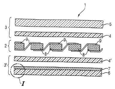
Fig. 1 shows the structure of the photovoltaic module 1
according to the invention, which consists of the solar cell
system 2 and the encapsulation materials 3, 3' enveloping the
solar cell systems. The solar cell systems 2 is made out of a
series of silicon cells 8, which are soldered in series to
form groups by means of bonding wires 9. The encapsulation
material 3' consists of the plastic sealing layer 4' and the
plastic film or plastic film composite 6, which exhibits the
oxide layer 7 separated out of the vapor phase on the surface
facing the solar cell system 2. This layer structure is
designed with "I'~. The encapsulation material 3 can be made
out of layer 5, for example, which can be a glass layer or
plastic film composite similar to 6, and a plastic sealing
layer 4.
Fig. a b additionally shows variants Ia and Ib, which can
replace the layer structure according to "I".
In variant Ia (Fig. la), the inorganic oxide layer 7 is
connected with an additional plastic film or plastic film
composite 11 via an adhesive layer 10 and/or a hybrid layer
comprised of organic/inorganic networks.
In variant lb (Fig. lb), the inorganic oxide layer 7 exhibits
an additional primer layer 12, which as a result establishes
the connection to the sealing layer 4'.
Fig. 2 shows an arrangement 13 for laminating the layers shown
in Fig. 1 for manufacturing the photovoltaic module 1
CA 02300828 2000-02-21
e~
'' according to the invention: It whose the loading station 14,
at which the module stack 1 can be placed on the carrier plate
15 moved by the transport system 16, as well as the vacuum
laminator 17 with the fixed upper part 18 and lower part 19
that can be raised and lowered using the hydraulic arrangement
20. Temperature, pressure and retention time are set in the
vacuum laminator 17 via control system 22. In addition, Fig. 2
shows the hardening furnace 23, whose temperature is set via
control system 24, the cooling area 25, whose temperature can
be set via control system 26, and the removal area 27.
Fig. 3 shows the air permeability of a plastic film 6
vapor-plated with an inorganic oxide layer 17 in different
wavelength ranges.
Fig. 4 shows the extent to which the photovoltaic module 1
according to the invention improves the barrier effect
relative to water vapor due to the oxide layer 7 separated
from the vapor phase.
_ CA 02300828 2000-02-21
~~0054367.doc
ONE WAY TO PERFORM THE INVENTION
The invention will now be described in more detail based on
embodiments.
In a first procedural step, the barrier layer 6 exhibiting the
inorganic oxide layer 7 is formed. In this case, the structure
can be selected based on the following table, with the
sequence running from the outside in, i.e., in the direction
of the solar cell system:
TABLE (Examples a-d):
Example a
- Barrier layer 6: Composite comprised of polyvinyl
fluoride (PVF), polyethylene terephthalate (PETP) in film
f o rm
- Inorganic oxide layer 7: SiOx or A1203
- Sealing layer 4'
Example b
- Barrier layer 6:
Plastic film comprised of ethylene tetrafluoroethylene
copolymer (ETFE)
- Inorganic oxide layer 7: SiOx or A1203
- Sealing layer 4'
Example c
- Barrier layer 6: Composite comprised of PVF and PETP
- Inorganic oxide layer 7: SiOx or A1203
- Hybrid layer comprised of organic/inorganic networks 10'
- Adhesive layer 10: e.g., polyurethane
- Plastic film or plastic film composite 11:
Polyvinyl fluoride (PVF), polyvinylidene fluoride (PVDF),
Ethylene tetrafluoroethylene copolymer (ETFE),
Poyethylene tereph~.halate (PETP)
- Sealing layer 4'
Example d
- Barrier layer 6: Composite comprised of PVF and PETP
- Inorganic oxide layer 7: SiOx or A1203
- Primer coat 12: e.g., polyurethane, ethylene vinyl
acetate (EVA), polymethyl methacrylate (PMMA)
- Sealing layer 4'
As evident from the table, the barrier layer 6 can consist of
a single plastic film according to Example b), and of a
plastic film composite according to Example a).
Preferably used as the sealing layers 9' are ethylene vinyl
acetate (EVA) films, which yield slightly during heat
treatment, as a result of which they become cross-linked,
which prevents the plastics from creeping.
Ionomers exhibit particularly good sealing properties. These
are polymers with ionic groups, which have a low water vapor
permeability in addition to good adhesive properties.
The inorganic oxide layer 7 is now generated on the PETP
plastic film (see Example a) per table) in a thickness of 30
to 200 nm through vapor separation under a vacuum (not shown).
A vacuum coating system (not shown) is used to this end, for
example. To ensure a satisfactory adhesion between the plastic
film surface and the inorganic oxide, the surface of the
plastic film is pretreated in a plasma consisting of oxygen
gas (99.995 o purity).
Stoichiometric quantities of aluminum oxide (99.9 o purity) or
silicon monoxide (99.9 o purity) are used as the coating
material, for example, and evaporated using electron beams
under a vacuum. The energy used during evaporation measured 10
keV, for example, at an emission rate of up to 220 mA. The
CA 02300828 2000-02-21
~0054367.doc Page 8
v J
thickness of the SiOx or A1203 layers can be set within a
range of 30 to 200 nm by varying the evaporation rate or speed
of the plastic films or plastic film composites moved via
rollers.
For example, a speed of 5 m/min is selected in the laboratory
for fabricating a 100 nm thick SiOx layer, while a speed of
2.5 m/min must be selected to manufacture a 40 nm thick A1203
layer. The evaporation rate here measured up to 70 nm/s; the
pressure used during evaporation was about 5x10⁻² Pa. During
industrial manufacture, speeds of 100 times or more faster can
be set.
The plastic film provided with the inorganic oxide layer, for
example made out of PETE, can now be laminated with the other
plastic film for manufacturing the plastic film composite, for
example made out of PVF (see Example a) per table).
The variants of the invention according to Examples a) and b)
now envisage that the inorganic oxide layer 7, preferably a
silicon oxide layer, be in direct contact with sealing layer
4', which ensures a satisfactory coupling. In this case, the
atomic ratio between silicon and oxygen can be varied as
desired.
CA 02300828 2000-02-21
~0054367.doc Page g
However, if the inorganic oxide layer, preferably the
silicon/oxide layer, in the photovoltaic module according to
the invention is intended to additionally ensure a UV
filtering effect, it is necessary to control the atomic ratio
of silicon to oxygen during evaporation in such a way that the
share of oxygen x lies between 1.3 and 1.7.
In addition to the above criteria, e.g., selection of the
starting products in a stoichiometric quantity ratio or
evaporation speed, this can also be accomplished by
additionally supplying oxygen in the form of a reactive gas
during evaporation. This gives rise to a highly transparent
oxide layer in the visible light wave range, which still
absorbs UV rays, so that the UV-sensitive sealing layers 4'
are also protected.
This is explained in greater detail in Fig. 3.
Fig. 3 shows the light permeability of an ETFE plastic film,
which exhibits a 320 nm thick SiOx layer as the inorganic
oxide layer. This makes it evident that the SiOx coated
plastic film is practically impermeable to light in the UV
range below 350 nm light wavelength. An uncoated plastic film
of the same constitution (not shown) would not absorb light in
this range, however. Starting at a light wavelength of 350 nm,
the ETFE film coated with SiOx starts to let the incident
light through. A significant transparence can be observed
starting at about 450 nm in the blue-violet portion of the
spectrum of visible light. A high transmission is observed
over the remaining visible light range, which only diminishes
again in the infrared range.
The following degrees of freedom are available to obtain
properties of the photovoltaic module according to the
invention, such as high light transmission in the visible and
near-UV range given a simultaneous blockage of light in the
shorter-wave UV range, and also a high barrier effect against
water vapor:
CA 02300828 2000-02-21
~0054367.doc Page 10
1. Variation of inorganic oxide layer thickness:
In this case, light permeability can be advantageously
influenced in good approximation according to the
Lambert-Beer's Law
ln(I/IO) - -4pkdl-1
where
I - light intensity allowed through
IO = radiated intensity,
k - wavelength-dependent absorption coefficient,
d - layer thickness of vapor-deposited inorganic oxide
layer,
light wavelength.
2. Variation of oxygen content (x) in the inorganic oxide
layer, preferably SiOx layer:
If x is increased from the value of 1.3 according to Fig. 3
using other vapor-deposition conditions, the transmission of
the material will be higher by the wavelength range of 400 nm
without having to change the layer thickness.
Values for x of 1.7, for example, can be set by adding oxygen
while simultaneously incorporating electromagnetic energy in
the form of microwave radiation.
Therefore, varying the layer thickness and oxygen content
parameters enable the simultaneous optimization of values for
transmission in the visible light range, the barrier effect in
the ultraviolet range, and the barrier effect relative to
water vapor.
In addition to the selective atomic ratio of silicon to
oxygen, resistance to atmospheric corrosion during outside use
of the photovoltaic module according to the invention is also
CA 02300828 2000-02-21
ensured by enveloping the inorganic oxide layer 7 on both
sides with plastic films or plastic film composites.
In Fig. 1, variant Ia, for example, this is done by having the
barrier layer 6 exhibit the inorganic layer 7, which in turn
is in contact with another plastic film or plastic film
composite 11 via adhesive layer 10. In this case, adhesive
layer 10 can be provided alone or in combination with a layer
10' comprised of hybrid layers of inorganic/organic networks.
These networks are inorganic/organic hybrid systems based on
alkoxy siloxanes, for example. They exhibit a close crosslink
density, and hence a high barrier effect relative to water
vapor, and at the same time adhere satisfactorily to the SiOx
layer.
Further, the plastic films according to Example c) can be
correspondingly selected from the table, so that they
additionally act to protect the solar cell system against
exposure to the elements. In this case, the arrangement for
the solar cell system according to Fig. 1/Ia can also be
selected in such a way that the barrier layer 6 is adjacent to
the sealing layer 4', while the plastic film or plastic film
composite 11 forms the outermost layer in the module stack.
In addition, it is also possible to bring about a satisfactory
resistance to atmospheric corrosion using a primer coat 12
made out of plastic, which is arranged between the sealing
layer 4' and the inorganic oxide layer 7 according to Fig.
1/variant Ib and Example d) from the table.
All variants can now be used in the laminating procedure with
the help of arrangement 13 according to Fig. 2 in order to
produce the photovoltaic module 1.
One variant will now be presented as an example.
The barrier layer 6 provided with the inorganic layer 7 is
layered with the plastic sealing layer 4', the solar cell
CA 02300828 2000-02-21
~0054367.doc Page 12
system 2, another plastic sealing layer 4 and the glass layer
5, as shown in Fig. 1. A PET/PVF plastic film composite can be
used in place of the glass layer 5.
Further, the layer 5, in particular when used outside, must be
resistant to atmospheric corrosion and decorative, so that
decorative laminate sheets provided with an acrylate layer and
designed MAX~ EXTERIOR are suitable.
This module stack is now incorporated into the arrangement 13
for lamination according to Fig. 2. In this case, the module
stack 1 is placed on the carrier plate 15 at the loading
station 14, which is kept at room temperature, or a maximal
temperature of 80 °C.
The top and bottom side of the module stack is provided with
separating films (not shown) to prevent adhesion to the
carrier plate 15 and remaining system parts.
After the module stack 1 has been placed on carrier plate 15,
the latter is conveyed into the vacuum laminator 17 via the
transport system 16, for example a chain conveyor. The
temperature of the heating plate 21 is kept at a level therein
corresponding to the softening point of the plastic materials
used in the sealing layer by means of an external control
system 22. The hydraulic arrangement 20 presses the heating
plate 21 against the carrier plate 15, so that the flow of
heat inside the carrier plate brings the plastics sealing
layers 4, 4' in the module stack to their softening point.
After the laminator 17 is closed, the external controller 22
applies a vacuum. The evacuation removes air and other
volatile constituents from the module stack, thereby ensuring
a blister-free laminate. This is followed by ventilation,
which presses the flexible membrane (not shown) against the
module stack.
After a defined retention time of the module stack 1 inside
CA 02300828 2000-02-21
-0054367.doc Pa a 13 .
the vacuum laminator 17, the latter is ventilated, and the
module stack is transported into the hardening furnace 23
without any additional pressing power. The latter is kept at a
defined temperature therein by the control system 24, so that
the sealing layers in the module stack harden after a defined
retention time, and a laminate is formed that is subsequently
cooled to room temperature in the cooling area 25. The
hardened laminate is take off of the carrier plate in the
removal area 27, and the recooled carrier plate can be routed
back to the loading station 14.
The photovoltaic module 1 according to the invention can
exhibit so-called thin-film solar cells instead of the
crystalline silicon cells. In this case, the solar cell system
can be connected with the encapsulation materials 3, 3' via
press molding or calendaring. These thin-film solar cells are
not susceptible to breaking, they are susceptible to water,
which makes the solution proposed in the invention
particularly worthwhile.
CA 02300828 2000-02-21
~0054367.doc
Page 14
The photovoltaic module stack can have the following
structure, for example:
Example e):
Layer 5: Glass
Solar cell system 2: Thin-film solar cell made out of
amorphous silicon
Sealing layer 4': EVA
Barrier layer 6: ETFE plastic film with inorganic SiOx
oxide layer 7
Example f):
Layer 5: Glass
Solar cell system 2: Thin-film solar cell made out of
amorphous silicon
Sealing layer 4': EVA
Barrier layer 6: PVF/PET plastic film composite and
inorganic SiOx oxide layer 7
In Examples e) and f), the thin-film solar cell system is
protected against water vapor by the barrier layer 6. However,
since the latter is not susceptible to breaking, the
additional sealing layer 4 can be omitted.
COMMERCIAL APPLICABILITY
The photovoltaic modules fabricated with the procedure
according to the invention are used for generating electrical
energy out of sunlight. They have various applications,
ranging from small power plants for emergency call boxes or
mobile homes via structurally integrated roof and fagade
systems, to large-scale plants and solar power facilities.
CA 02300828 2000-02-21
~0054~67.doc
Pale 15
With respect to outside applications, it has been shown that
the barrier effect relative to water vapor is significantly
improved by the oxide layer separated out of the vapor phase.
Fig. 4 explains this in greater detail.
In this case, uncoated films (left column on abscissa) were
compared with SiOx coated films (right column on the abscissa)
with respect to their water vapor permeability in g/m2d.
As evident from this comparison, the water vapor permeability
could be reduced to about one tenth the value of the uncoated
material for type RN 12 PET, and to 1/25 for type RN 75. The
water vapor permeability is even reduced by a factor of about
100 for ETPE with a material thickness of 20 rm.
CA 02300828 2000-02-21