Note : Les descriptions sont présentées dans la langue officielle dans laquelle elles ont été soumises.
CA 02305346 2000-03-28
WO 99/19755 PCTNS98/20042
OPTICAL DEVICE HAVING OPTICAL COMPONENT ISOLATED FROM HOUSIN
This application claims priority to U.S. Patent Application 60/061,688 filed
on
October 10, 1997, which is hereby incorporated by reference.
FIELD OF THE INVENTION
The present invention relates to an optical device and, more particularly, to
an
optical device having an optical component isolated from a housing.
DESCRIPTION OF THE RELATED ART
A reflective or Bragg grating, which reflects light over a narrow wavelength
band, can be established in an optical waveguide fiber (optical fiber) by
known methods
to produce a precise optical waveguide component that typically has channel
spacings
measured in nanometers. Such a fiber Bragg grating component can be used, for
example, as a filter in a telecommunications system.
A change in the temperature of the grating region of the optical fiber can
shift the central wavelength of the fiber Bragg grating component because of
changes in
glass refractive index and physical expansion of the fiber. Thus, the fiber
Bragg grating
2o component can exhibit wavelength variability over a range of operating
temperatures.
This temperature-induced variability can create practical difficulties in the
use of the
fiber Bragg grating component.
One method of passively athermalizing the fiber Bragg grating component
involves changing the tension in the grating region of the optical fiber in
response to
CA 02305346 2000-03-28
WO 99/19755 PCT/US98/20042
2
temperature change. More specifically, since changing the tension in the
grating region
can shift the central wavelength of the fiber Bragg grating component, the
central
wavelength shift caused by temperature change can be offset by an appropriate
change
in the tension in the grating region.
This passive athermalization method can be implemented by attaching the
optical
fiber, under appropriate tension, to a substrate having a suitable negative
temperature
coefficient of thermal expansion. With a proper choice of design parameters,
wavelength shift due to temperature change can be greatly reduced by an
offsetting
change in tension caused by a dimensional change in the substrate.
1o The fiber Bragg grating component is disposed in a housing to form an
optical
device in which the fiber Bragg grating component is protected from the
environment.
Conventionally, the substrate of the fiber Bragg grating component is
connected directly
to the housing by an adhesive covering an area on the substrate that averages
about 80
square millimeters (nvn2), but can vary from 40 to 400 mm2, with a thickness
typically
15 between 0.1 to 0.5 millimeters (mm).
Environmental testing, which involves monitoring the optical performance while
cycling the temperature between -40°C and 85°C, has shown that
the central wavelength
of the fiber Bragg grating component still shifts in an undesirable manner in
response to
temperature changes. This shift in the central wavelength may be caused, at
least in
2o part, by mechanical coupling of the substrate of the fiber Bragg grating
component to
the housing, which produces unwanted strain in the substrate when the housing
undergoes dimensional changes caused by variations in ambient conditions, such
as
temperature and humidity.
25 SUMMARY OF THE INVENTION
An object of the present invention is to provide an optical device that solves
the
foregoing problems.
CA 02305346 2000-03-28
WO 99/19755 PCT/US98/20042
3
Another object of the present invention is to provide an optical device having
a
housing and an optical waveguide component that is substantially isolated or
uncoupled
from the housing.
Additional objects and advantages of the invention will become apparent from
the description which follows. Additional advantages may also be learned by
practice of
the invention.
In a broad aspect, the invention provides an optical device including an
optical
waveguide component, a housing for the optical waveguide component, and a
connecting portion that attaches the optical waveguide component to the
housing while
l0 substantially completely isolating the optical waveguide component from
force imposed
on the connecting portion due to a dimensional change of the housing caused by
a
variation in ambient conditions.
In an additional aspect, the invention includes the method of making the
inventive optical device, including the method of isolating the optical
component.
It is to be understood that both the foregoing summary and the following
detailed description are exemplary and explanatory only and are not
restrictive of the
invention, as claimed.
BRIEF DESCRIPTION OF THE DRAWINGS
The invention will be described in conjunction with the accompanying drawings,
which illustrate embodiments of the invention.
FIG. 1 is a sectional view of a first embodiment of an optical device
according to
the present invention.
FIG. 2 is a sectional view of the first embodiment of the optical device taken
along line 2-2 of FIG. 1.
FIG. 3 is a sectional view of a second embodiment of an optical device
according
to the present invention.
FIG. 4 is a sectional view of the second embodiment of the optical device
taken
along line 4-4 of FIG. 3.
CA 02305346 2000-03-28
WO 99/19755 PCTNS98/20042
4
FIG. 5 is a sectional view of a third embodiment of an optical device
according
to the present invention.
FIG. 6 is a sectional view of the third embodiment of the optical device taken
along line 6-6 of FIG. 5.
FIG. 7 is a graphic comparison of the wavelength shift caused by applying
force
to a fiber Bragg grating component, a conventional optical device with a fiber
Bragg
grating component, and an optical device with fiber Bragg grating component
according
to the present invention.
DESCRIPTION OF THE PREFERRED EMBODIIyyIENTS
to
Reference will now be made in detail to the preferred embodiments of the
invention.
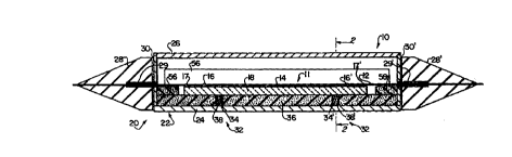
As shown generally in FIGS. 1, 3, and 5, an optical device 10, 40, SO
according
to the present invention comprises an optical waveguide component 1 l, a
housing 20 for
the optical waveguide component 1 l, and a connecting portion 32, 42, 52 that
attaches
the optical waveguide component 11 to the housing 20 while substantially
completely
isolating the optical waveguide component 11 from force imposed on the
connecting
portion 32, 42, 52 due to a dimensional change of the housing 20 caused by a
variation
in ambient conditions. The variation in ambient conditions could be, for
example, a
2o temperature or humidity change or a change in an external force imposed on
the housing
20.
In each of the first through third embodiments, the optical waveguide
component
11 includes an optical fiber 12 having a Bragg grating formed by conventional
means in
a grating region 14 extending for a portion of the fiber 12 between spaced
frits 16 and
16', which hold the optical fiber 12 on a mounting member 18 under tension.
Spaced
epoxy attachments 17 and 1 T grip the optical fiber so that longitudinal
forces imposed
on the optical fiber do not affect the grating region 14. The mounting member
18 is
preferably formed of a beta-eucryptite glass-ceramic, which has a negative
temperature
coefficient of thermal expansion and thus passively athermalizes the optical
waveguide
3o component 11. The mounting member 18 could also be constituted by an
arrangement
CA 02305346 2000-03-28
WO 99/19755 PCTNS98/20042
of dissimilar materials constructed so as to impart an effective negative
coefficient of
thermal expansion on the optical fiber 12.
The housing 20 includes a casing portion 22, which has a base 24 and a lid 26.
The casing portion 22 is typically bolted to a substrate (not shown). The
housing 20
also includes two rubber end pieces 28 and 28', which are fitted over solder
extensions
29 and 29' extending from the base 24. The rubber end pieces 28 and 28' are
connected
to sides of the base 24 by layers of a suitable adhesive 30 and 30'. The
rubber end pieces
28 and 28' help to prevent the optical fiber 12 from bending proximate housing
20. The
rubber end pieces 28 and 28' provide for a finite bend radius of the optical
fiber 12 if a
lateral load is imparted to the optical fiber 12 external to the housing 20.
The casing portion 22 of the housing 20 is preferably hermetic and formed of a
material with low thermal expansion. Presently, gold-coated KOVAR~, which is a
commercially available metal alloy, is the preferred low thermal expansion
metal material
for forming the casing portion 22. KOVAR~ is an iron-nickel-cobalt alloy (29%
Ni -
17% Co - 53% Fe) that has a nominal expansion coefficient of approximately 5
ppm/°C
(T.E.C. 5 x 10⁶ at 20-400°C) inflection temperature of about
450°C with an 1V1'
temperature less than -80°C. Dilver-P alloy produced by Imphy, S.A., is
a competitive
grade with KOVAR~ alloy of Carpenter Steel.
The casing portion 22 can also be formed of a molded material. For example,
2o casing portion 22 can be formed by molding a liquid crystal polymer, such
as
VECTRA~. Like most such materials, the thermal expansion of VECTRA~ is quite
anisotropic, being strongly influenced by flow conditions during the molding
operation.
Thus, over time, temperature and humidity changes can cause the molded casing
portion
22 to permanently bend or twist (warp). Temperature and humidity changes over
time
can also cause permanent linear dimensional changes of the molded casing
portion 22.
In conventional optical devices, the permanent warpage and linear dimensional
changes
typically occur after the optical waveguide component has been connected to
the
molded casing portion and thus cause an undesirable force to be imposed on the
optical
waveguide component.
CA 02305346 2000-03-28
WO 99/19755 PCT/US98/20042
6
In accordance with the present invention, the molded casing portion 22 can be
subjected to post-molding annealing (preferably at 125 to 135°C for 4
to 18 hours for
VECTRA~) to cause the permanent warpage and linear dimensional changes to
occur
before insertion of the optical waveguide component 11. Post-molding annealing
s therefore significantly decreases the permanent dimensional changes, caused
by a
variation in ambient conditions, that occur after the optical waveguide
component I 1
has been connected to the housing 20.
For example, a 2.5 inch long VECTRA~ molded casing portion was annealed at
125°C for 16 hours, resulting in a permanent length decrease of 0.050
inches (about
0 2%). Thereafter, the molded casing portion did not undergo any substantial
permanent
warpage or linear dimensional changes.
In the first embodiment shown in FIGS. 1 and 2, the connecting portion 32
includes two discrete bodies of adhesive 34 and 34' that are bonded to the
optical
waveguide component 11 and the housing 20. The adhesive bodies 34 and 34'
Is preferably have a shear modulus and dimensions such that the optical
waveguide
component 11 is substantially completely isolated from force imposed on the
adhesive
bodies 34 and 34' by the housing 20. More preferably, the adhesive bodies 34
and 34'
include an adhesive with a low shear modulus (less than 1000 pounds per square
inch
(psi)) over the typical operating temperatures of-40°C to 85°C.
A particular silicone
2o adhesive meeting this requirement is RTV-3145 (Dow Corning), which has a
shear
modulus that varies from 1 SO psi at -40°C to about 75 psi at
80°C, and is about 100 psi
at room temperature. Preferably the area of a portion of the optical waveguide
component 11 bonded or fixed to a. corresponding one of the bodies of adhesive
34 and
34' is about 2.5 to 15 mm2 (total area of about S to 30 mm2 for both bodies of
adhesive),
2s and the thickness of the bodies of adhesive 34 and 34' in a direction
extending between
the optical waveguide component 11 and the housing 20 is approximately 1.2 mm.
The
bodies of adhesive 34 and 34' are preferably located as close to the center of
the
mounting member 18 as possible, while still being able to assure adhesion
under
conditions of mechanical shock and vibration, such as during shock testing.
CA 02305346 2000-03-28
WO 99/19755 PCT/US98/20042
7
The optical device 10 of the first embodiment further includes a spacer member
36 disposed between the optical waveguide component 11 and the housing 20. The
spacer member 36 is not bonded to the optical waveguide component 11 or the
housing
20. Although the spacer member 36 could be rigid, it preferably is flexible
and has a low
shear modulus over the typical operating temperatures and, more preferably,
includes an
elastomeric foam. A presently-preferred foam is PORON~ 52000 silicone foam
(Rogers Corporation), which was a shear modulus of 2 psi. The spacer member 36
has
two holes 38 and 38' that accommodate the two bodies of adhesive 34 and 34',
respectively.
1o Optical devices 10 can be manufactured uniformly and conveniently by
placing
the spacer member 36 having holes 38 and 38' in the casing portion 22 before
inserting
the bodies of adhesive 34 and 34'. Specifically, the spacer member 36 serves
as a mold
for the bodies of adhesive 34 and 34', with the thickness of the spacer member
36
determining the thickness of the bodies of adhesive 34 and 34', and the holes
38 and 38'
controlling the width and location of the bodies of adhesive 34 and 34'.
Therefore,
optical devices 10 having uniformly sized and located bodies of adhesive 34
and 34' can
be readily manufactured by using uniformly-dimensioned spacer members 36 and
by
using a precisely metered volume of adhesive.
In the second embodiment shown in FIGS. 3 and 4, the bodies of adhesive 34
and 34' are not used. Instead, the connecting portion 42 includes a flexible
support
member 44 disposed between the mounting member 18 of the optical waveguide
component 11 and the housing 20 and bonded to them by layers of adhesive 46
and 48.
The support member 44 preferably has a shear modulus and dimensions such that
the
optical waveguide component 11 is substantially completely isolated from force
imposed
on the support member 44 by the housing 20. More preferably, the support
member 44
has a very low shear modulus (less than 100 psi) over the typical operating
temperatures. Even more preferably, the support member 44 includes an
elastomeric
foam, such as PORON~ 52000 silicone foam. The thickness of the support member
44
in a direction extending between the optical waveguide component 11 and the
housing
20 is preferably about 0.8 mm.
CA 02305346 2000-03-28
WO 99/19755 PCT/US98/20042
8
The layers of adhesive 46 and 48 bond at least a portion of the upper surface
of
the support member 44 to the mounting member 18 of the optical waveguide
component
11 and bond at least a portion of the lower surface of the support member 44
to the
housing 20, respectively. The adhesive is preferably RTV-3145, although other
adhesives, such as pressure sensitive adhesives, may be used. In the preferred
embodiment, the total area of the optical waveguide component 11 (which is
typically
about 200 mm2) is bonded or fixed to the portion of the surface of the support
member
44.
In the third embodiment shown in FIGS. 5 and 6, the connecting portion 52 is
to constituted by a gel 54. The gel 54 preferably has a shear niodulus and
dimensions such
that the optical waveguide component 11 is substantially completely isolated
from force
imposed on the gel 54 by the housing 20. More preferably, the gel 54 has a
very low
shear modulus (less than 100 psi) over the typical operating temperatures.
Gels meeting
this requirement include General Electric silicone gels RTV-6126, RTV-6136,
RTV-
6156, and RTV-6166, which all have a shear modulus of less than 2 psi. The
optical
waveguide component 11 can be secured to the housing 20 by placing the uncured
gel
54 in the housing 20, inserting the optical waveguide component 11 into the
gel 54, and
curing the gel 54 by conventional means such as heat or ultraviolet radiation.
The total
area of the bottom surface of the optical waveguide component 11 is bonded or
fixed to
2o the gel 54 in the preferred embodiment, and the thickness of the gel 54 in
a direction
extending between the optical waveguide component 11 and the housing 20 is
about 0.8
The presently preferred embodiments of the invention do not include force
absorbing members 56, yet the first and second embodiments may fi~rther
comprise force
absorbing members 56 disposed between the optical waveguide component 11 and
respective sides of the housing 20 to provide shock absorbing capability
during use of
the optical device 10, 40. The force absorbing members 56 are preferably
formed of a
silicone material such as PORON~ S2000 foam or a solid silicone rubber. The
force
absorbing members 56 are preferably glued to one of the base 24 or the
mounting
3o member 18 by a suitable adhesive.
CA 02305346 2000-03-28
WO 99/19755 PCTNS98/20042
9
Having described preferred implementations of the invention, it is appropriate
to
address principles underlying the foregoing and other implementations of the
invention.
It has been determined, in connection with the present invention, that the
optical
waveguide component 11 can be substantially completely isolated from force
imposed
on the connecting portion 32, 42, 52 due to a dimensional change of the
housing 20 by
utilization of the following equation based on Hooke's Law of linear
elasticity:
Fo = (d x A x G')lt
where:
Fo: force imposed on the optical waveguide component 11;
1o d: displacement of the housing 20 relative to an initial position
(determined
at the time of connecting the optical waveguide component 11 to the
housing 20) due to a dimensional change of the housing 20 caused by a
variation in ambient conditions;
A: total area of a portion or portions of the optical waveguide component
11 fixed to the connecting portion 32, 42, 52;
G': shear modulus of the connecting portion 32, 42, 52; and
t: thickness of the connecting portion 32, 42, 52 in a direction extending
between the optical waveguide component 1 l and the housing 20.
As is evident from this equation, the force Fo transferred from the housing 20
to
2o the optical waveguide component 11 by the connecting portion 32, 42, 52 is
a function
of the displacement d, the area A, the shear modulus G', and the thickness t.
The force
Fo can be reduced by reducing the displacement d, the area A, or the shear
modulus G'
or by increasing the thickness t.
In the f rst embodiment, the force Fo transferred to the optical waveguide
component 11 through the connecting portion 32 is reduced by reducing the area
A and
increasing the thickness t. More specifically, the total area A of the
portions of the
optical waveguide component 11 fixed to the bodies of adhesive 34 and 34'
(preferably
about 5 to 30 mm2) is significantly smaller than the total area of the portion
of the
optical waveguide component fixed to the adhesive in conventional optical
devices
(typically 80 mm2). Also, the thickness t of the bodies of adhesive 34 and 34'
(preferably
CA 02305346 2000-03-28
WO 99/19755 PCTNS98/20042
about 1.2 mm) is significantly larger than in conventional optical devices
(typically 0. I to
0.5 mm).
In the second and third embodiments, the force Fo transferred to the optical
waveguide component 11 is reduced by reducing the shear modulus G' and
increasing
5 the thickness t. Specifically, the shear modulus G' of the support member 44
and the gel
54 (preferably less than about 2 psi) is significantly smaller than the shear
modulus of the
adhesive used in conventional optical devices (typically 100 to 1,000,000
psi). Also, the
thicknesses t of the support member 44 and the gel 54 (each preferably about
0.8 mm)
are significantly larger than in conventional optical devices (typically 0.1
to 0.5 mm).
to In an embodiment of the invention using a molded casing portion 22, the
force Fo
imposed on the optical waveguide component I I can also be reduced by
reducing,
relative to conventional optical devices, the displacement d of the housing
20. More
specifically, annealing the molded casing portion 22 significantly decreases
permanent
dimensional changes (displacement d) that would otherwise occur after the
optical
waveguide component 1 I had been connected to the housing 20.
In a more preferred aspect of the present invention, the displacement d, the
area
A, the shear modulus G', and the thickness t are adjusted to limit the force
Fo such that it
satisfies the following condition:
Fo c 0.10(Fn)
2o where:
Fn: force imposed on the connecting portion 32, 42, 52 due to a dimensional
change of the housing caused by a variation in ambient conditions.
Although the isolation of the optical waveguide component 11 from the housing
has been described in connection with linear displacement of the housing 20,
the
present invention can isolate the optical waveguide component 11 from forces
on the
connecting portion due to other dimensional changes of the housing 20, such as
twisting
or bending. Those forces can be determined by the well-known principle of
superposition.
The ability of an optical device according to the present invention to
substantially
3o completely isolate the optical waveguide component 11 from force imposed on
the
CA 02305346 2000-03-28
WO 99/19755 PCT/US98/20042
connecting portion 32, 42, 52 due to a dimensional change of the housing 20 is
demonstrated in FIG. 7, which shows the results of an experiment involving
three optical
devices. The first optical device was an unhoused, conventional fiber Bragg
grating .
component having a beta-eucryptite glass-ceramic mounting member. The second
optical device included the same type of conventional fiber Bragg grating
component,
but it was glued in the conventional manner (RTV-3145 silicone having an area
A = 80
mmz and a thickness t = 0.4 mm) to a housing formed of VECTRA~. The third
optical
device included the same type of conventional fiber Bragg grating component,
but it was
connected to a housing formed of VECTRA~ by a connecting portion in accordance
1o with the first embodiment of the present invention (two bodies of RTV-3145
silicone
adhesive with a total area A = 17 mm2 and a thickness t = 0.8 mm).
Each of the optical devices was subjected to three-point, flexure testing,
which
involved supporting each optical device on opposite ends of its bottom surface
and
subjecting it to forces (i.e., changes in ambient conditions) imposed
transversely to the
optical device on the center of its top surface. The central wavelengths of
the optical
devices were measured as the forces were imposed.
As shown in FIG. 7, the central wavelength of the unhoused fiber Bragg grating
component shifted by a significant amount in response to force. The central
wavelength
of the conventionally-housed fiber Bragg grating component shifted by a
lesser, but
2o nonetheless unacceptable, amount. The central wavelength of the optical
device
according to the present invention barely shifted.
In the optical device according to the present invention, the optical
waveguide
component is substantially completely isolated from force imposed on the
connecting
portion due to a dimensional change of the housing. In other words, the
optical
waveguide component is not subjected to loads under normal operating
conditions that
will cause its optical performance to deviate from acceptable tolerances.
It will be apparent to those skilled in the art that various modifications and
variations can be made in the apparatus of the present invention without
departing from
the scope or spirit of the invention. For example, although preferred
embodiments have
3o been described with reference to an optical waveguide component having a
Bragg
CA 02305346 2000-03-28
WO 99!19755 PCT/US98/20042
12
grating, certain aspects of the invention may be applied to other optical
waveguide
components that are adversely affected by forces imposed thereon. A specific
example
is an optical waveguide component including an optical fiber with a long-
period grating
mounted on a mounting member (preferably a low-expansion substrate such as
fused
silica) to maintain constant tension in the grating over a temperature range.
A long-
period-grating component can be adversely affected by forces transferred from
the
housing and thus can benefit from the present invention. Certain aspects may
also be
applied to other suitable optical waveguide components, such as optical
couplers or
amplifiers.
As a further example, although the optical device of the first embodiment
includes the spacer member having two holes, the spacer member could have one
large
hole for receiving the bodies of adhesive, or the spacer member could be
eliminated
altogether. As yet another example, although the optical waveguide component
in the
third embodiment is disposed on top of the gel, it could also be completely
enveloped by
the gel.
The invention further includes the method of making the inventive optical
device
wherein the optical component is isolated from the housing. The inventive
method
includes the isolating of the optical component from the housing and other
steps utilized
in making the described inventive optical device.
2o Other embodiments of invention will be apparent to those skilled in the art
from
consideration of the specification and practice of the invention disclosed
herein. It is
intended that the specification and examples be considered as exemplary only,
with a
true scope and spirit of the invention being indicated by the following
claims.