Note : Les descriptions sont présentées dans la langue officielle dans laquelle elles ont été soumises.
CA 02316253 2000-06-27
1
SPECIFICATION
OPTICAL WAVELENGTH DIVISION MULTIPLEXING TRANSMISSION
NETWORK SYSTEM USING TRANSMITTING/RECEIVING APPARATUSES
HAVING 2-INPUT AND 2-OUTPUT OPTICAL PATH SWITCHING ELEMENTS
TECHNICAL FIELD
The present invention relates to a full-mesh optical wavelength division
multiplexing transmission network system for transmitting a plurality of
wavelength-multiplexed optical signals between a plurality of
transmitting/receiving
apparatuses.
BACKGROUND ART
In an optical wavelength division multiplexing (WDM) transmission system for
transmitting a plurality of optical signals through a single optical fiber by
assigning
different wavelengths to each optical signal, it is possible not only to
remarkably
increase the capacity of the transmission path, but also to perform the
"wavelength-addressing" operation in which information about the addressee of
the
relevant signal corresponds to each wavelength itself.
A star-topology WDM system includes an arrayed-waveguide grating type
multiplexing/demultiplexing circuit (or arrayed-waveguide grating type
multi/demultiplexer) in the center of the system, where this
multiplexing/demultiplexing circuit has a wavelength response having a cyclic
input/output relationship, and makes it possible to connect N
transmitting/receiving
apparatuses with each other. According to such a star-type WDM system, it is
possible to realize a full-mesh WDM transmission network system only by using
optical
signals of N wavelengths, in which each of N x N signal paths for connecting
the
CA 02316253 2000-06-27
2
apparatuses with each other can be independently connected.
Fig. 4 is a schematic diagram showing the structure of a conventional full-
mesh
WDM transmission network system.
In the figure, reference numerals 1 to 7 indicate the 1st to Nth
transmitting/receiving apparatuses (the 7th to (N-1)th apparatuses are not
shown) for
transmitting and receiving a WDM (wavelength-division-multiplexed) signal (of
wavelengths ~,, to ~.n), reference numeral 8 indicates an N x N arrayed-
waveguide
grating type multiplexing/demultiplexing circuit (AWG) having N input and N
output
ports and having a wavelength response which has a cyclic input/output
relationship.
Fig. 5 is a diagram showing the general structure of the full-mesh WDM
transmission network system in Fig: 4.
In Fig. 5, reference numerals 9 to 12 indicate the 1st to Nth
transmitting/receiving apparatuses (the ith apparatus indicates any of the
omitted
apparatuses in the figure), reference numeral 13 indicates a receiver for
receiving a
WDM signal (of wavelengths ~,1 to 7~~), reference numeral 14 indicates a
transmitter for
transmitting a WDM signal (of wavelengths ~,1 to ~,"), reference numeral 15
indicates a
demultiplexer for demultiplexing a WDM signal transmitted through a single
optical
fiber, reference numeral 16 indicates a multiplexer for multiplexing a
plurality of optical
signals having different wavelengths transmitted from the transmitter 14 so as
to
transmit a signal through a single optical fiber, reference numeral 17
indicates an N x N
arrayed-waveguide grating type multiplexing/demultiplexing circuit (AWG), and
reference numerals 18 to 21 indicate optical fibers for optically connecting
the
transmitting/receiving apparatuses 9 to 12 and the input and output ports of
AWG 17.
Here, the structure of each transmitting/receiving apparatus (10 to 12) is the
same as
the transmitting/receiving apparatus 9.
Fig. 6 is a diagram showing the wavelength response having a cyclic
input/output relationship, and the connection relationship between the
transmitting/receiving apparatuses and the AWG ports in the conventional full-
mesh
CA 02316253 2000-06-27
3
WDM transmission network system. For a simple explanation, the case using an 8
x
8 AWG is shown in Fig. 6.
Between 8 input ports and 8 output ports of the AWG, (8 x 8 =) 64 paths can
be established; however, the cyclic characteristic as shown in Fig. 6 makes it
possible
to independently establish 64 paths using the minimum 8 wavelengths. The above
input and output ports of the AWG are connected to each relevant
transmitting/receiving apparatus, so that each signal can be independently
transmitted
via any possible path between the eight transmitting/receiving apparatuses.
Here, a
specific wavelength ~.; is assigned to each path. Therefore, it is possible to
perform
the wavelength addressing operation in which when the wavelength corresponding
to a
target receiver is selected at the transmitter side, a signal is automatically
transmitted
to the target receiver.
Fig. 7 is a diagram for explaining the wavelength addressing operation. In the
figure, reference numerals 22 to 29 indicate 8 transmitting/receiving
apparatuses, and
reference numeral 30 indicates an 8 x 8 AWG. The wavelength response of the
AWG
and the connection relationship between the AWG ports and each
transmitting/receiving apparatus are the same as those shown in Fig. 6.
The optical signal of wavelength ~,~ transmitted from the 1st
transmitting/receiving apparatus 22 is introduced to input port 1 of AWG 30,
and is
output from output port 2 to the 2nd transmitting/receiving apparatus by
switching the
optical signal in the AWG 30 according to its wavelength. Similarly, the
response
signal of wavelength ~,7 transmitted from the 2nd transmitting/receiving
apparatus 23 is
transmitted to the 1st transmitting/receiving apparatus 22 via AWG 30. In
addition,
the optical signals having wavelengths ~,z and ~,$ are respectively and
automatically
transmitted to the 5th transmitting/receiving apparatus 26 and the 3rd
transmitting/receiving apparatus 24.
However, in the above conventional full-mesh WDM transmission network
system, the addressee of the target signal one-to-one corresponds to a
wavelength;
CA 02316253 2000-06-27
4
therefore, if the transmitter relating to the relevant wavelength or the
semiconductor
laser used as a light source is damaged, a signal cannot be transmitted to a
target
receiver. Also if the receiver relating to the relevant wavelength is damaged,
a
similar problem occurs. These problems are serious for suitably operating and
managing the system. Furthermore, in a conventional system, it is impossible
to
temporarily increase the transmission capacity between specific
transmitting/receiving
apparatuses.
DISCLOSURE OF THE INVENTION
In consideration of the above problems, an objective of the present invention
is
to provide a full-mesh optical wavelength division multiplexing transmission
network
system for suitably coping with a damaged transmitter or receiver
corresponding to a
specific wavelength, and for temporarily increasing the transmission capacity
between
specific transmitting/receiving apparatuses in case of need.
To achieve the above objective, the present invention provides an optical
wavelength division multiplexing transmission network system comprising:
an arrayed-waveguide grating type multiplexing/demultiplexing circuit having,
N input ports and N output ports, where N is a plural number; and
N transmitting/receiving apparatuses, each apparatus being optically connected
to a predetermined input port and a predetermined output port of the
arrayed-waveguide grating type multiplexing/demultiplexing circuit, wherein:
the arrayed-waveguide grating type multiplexing/demultiplexing circuit has a
wavelength response having a cyclic input/output relationship; and
each transmitting/receiving apparatus comprises:
a demultiplexer for demultiplexing an optical signal input from the
predetermined output port of the arrayed-waveguide grating type
multiplexing/demultiplexing circuit into signals of N wavelengths, and
respectively
outputting the demultiplexed optical signals from N output ports;
CA 02316253 2000-06-27
a transmitter for respectively transmitting optical signals of N
wavelengths from N output ports;
a receiver for respectively receiving optical signals of N wavelengths
from N input ports;
a multiplexer for multiplexing optical signals of N wavelengths input
from N input ports, and outputting the multiplexed signal to the predetermined
input
port of the arrayed-waveguide grating type multiplexing/demultiplexing
circuit; and
N 2-input and 2-output optical path switching elements corresponding
to N wavelengths, each switching element being independently switched between
first
and second connective conditions, wherein:
in the first connective condition, the output port corresponding to a
specific wavelength of the demultiplexer is connected to the input port
corresponding
to the specific wavelength of the receiver, and the output port corresponding
to a
specific wavelength of the transmitter is connected to the input port
corresponding to
the specific wavelength of the multiplexer; and
in the second connective condition, the output port corresponding to a
specific wavelength of the transmitter is connected to the input port
corresponding to
the specific wavelength of the receiver, and the output port corresponding to
a specific
wavelength of the demultiplexer is connected to the input port corresponding
to the
specific wavelength of the multiplexer.
According to the present invention, an optical signal transmitted to the
demultiplexer of a relevant transmitting/receiving apparatus via the switching
operation of the arrayed-waveguide grating type multiplexing/demultiplexing
circuit
according to the wavelength of the optical signal can be returned by using the
relevant
2-input and 2-output optical path switching element in the
transmitting/receiving
apparatus so that the returned signal is transmitted via the multiplexer to
the
arrayed-waveguide grating type multiplexing/demultiplexing circuit again. This
optical signal is re-switched in the arrayed-waveguide grating type
CA 02316253 2000-06-27
6
multiplexing/demultiplexing circuit according to the wavelength, and is
transmitted to
another transmitting/receiving apparatus.
That is, when an optical signal is transmitted from the transmitter of one of
the
transmitting/receiving apparatuses to (the receiver of) a target
transmitting/receiving
apparatus (i.e., addressee), even if the transmitting or receiving portion
corresponding
to the relevant wavelength is damaged, an optical signal can be bypassed and
transmitted to the target receiver by (repeatedly) performing the signal-
returning
operation as explained above.
In addition, according to the above structure, a plurality of signal paths can
be
temporarily established between specific transmitting/receiving apparatuses by
switching the connective condition of each 2-input and 2-output optical path
switching
element, thereby temporarily increasing the transmission capacity.
As a preferable example, in the connection between the arrayed-waveguide
grating type multiplexing/demultiplexing circuit and the
transmitting/receiving
apparatuses, the ith input port and the (N - i + 1)th output port of the
arrayed-waveguide grating type multiplexing/demultiplexing circuit are
respectively
connected to the multiplexer and the demultiplexer of the ith
transmitting/receiving
apparatus via an optical fiber, where i is an integer from 1 to N.
In addition, each of the N 2-input and 2-output optical path switching
elements
may be a thermo-optic switch using the thermo-optic effect of a silica-based
planar
lightwave circuit.
BRIEF DESCRIPTION OF THE DRAWINGS
Fig. 1 is a diagram showing the general structure of an embodiment of the
optical wavelength division multiplexing transmission network system according
to the
present invention.
Fig. 2 is a diagram showing the wavelength response which has a cyclic
input/output relationship of the AWG and the connection relationship between
the
CA 02316253 2000-06-27
7
transmitting/receiving apparatuses and the ports of the AWG in the embodiment.
Fig. 3 is a diagram for explaining an operation example of the optical
wavelength division multiplexing transmission network system in the
embodiment.
Fig. 4 is a schematic diagram showing the structure of a conventional full-
mesh
WDM transmission network system.
Fig. 5 is a diagram showing the general structure of the conventional full-
mesh
WDM transmission network system.
Fig. 6 is a diagram showing the wavelength response having a cyclic
input/output relationship, and the connection relationship between the
transmitting/receiving apparatuses and the AWG ports in the conventional
system.
Fig. 7 is a diagram for explaining an operation example of the conventional
optical wavelength division multiplexing transmission network system.
MODES FOR CARRYIT1G OUT THE INVENTION
Hereinbelow, preferred embodiments of the present invention will be
explained with reference to the drawings.
Fig. 1 is a diagram showing of an embodiment of the general structure of the
optical wavelength division multiplexing (WDM) network system according to the
present invention.
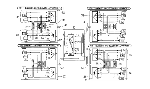
In Fig. 1, reference numerals 31 to 34 indicate the 1st to Nth
transmitting/receiving apparatuses (the ith apparatus indicates any of the
omitted
apparatuses in the figure), reference numeral 35 indicates a transmitter for
transmitting a WDM (wavelength-division-multiplexed) signal (of wavelengths
~,1 to ~,~),
reference numeral 36 indicates a receiver for receiving a WDM signal (of
wavelengths
~,1 to ~,~), reference numeral 37 indicates a multiplexer for multiplexing a
plurality of
optical signals having different wavelengths so as to make a signal
transmitted through
a single optical fiber, reference numeral 38 indicates a demultiplexer for
demultiplexing
a WDM signal transmitted through a single optical fiber, reference numeral 39
CA 02316253 2000-06-27
8
indicates a switching section including N switches, that is, 2-input and 2-
output optical
path switching elements 39, to 39N, for switching and supplying optical
signals from the
transmitter 35 and optical signals from the demultiplexer 38 to the receiver
36 and
multiplexer 37, reference numeral 40 indicates an N x N arrayed-waveguide
grating
type multiplexing/demultiplexing circuit (AWG), and reference numerals 41 to
44
indicate optical fibers for optically connecting the transmitting/receiving
apparatuses 31
to 34 and the input and output ports of AWG 40. Here, the structure of each of
the
2nd to Nth transmitting/receiving apparatuses (32 to 34) is the same as the
1st
transmitting/receiving apparatus 31.
In the present embodiment, a 1 x N AWG is used for each of the multiplexer
37 and the demultiplexer 38, and each of the 2-input and 2-output optical path
switching
elements 391 to 39N is realized by using a 2 x 2 thermo-optic switch (TOSW)
using the
thermo-optic effect of a silica-based planar lightwave circuit (i.e., silica-
based PLC).
When each 2 x 2 TOSW (391 to 39N) is operated in the cross mode, the optical
signals from the transmitter 35 are introduced to the multiplexer 37 while the
optical
signals from the demultiplexer 38 are introduced to the receiver 36. Usually,
the 2 x
2 TOSW is operated in this cross mode.
When each 2 x 2 TOSW is operated in the bar mode, the optical signals from
the demultiplexer 38 are introduced to the multiplexer 37 so that the relevant
signal is
returned to optical fiber 41 connected to the AWG 40. In addition, the optical
signals
from the transmitter 35 are returned to the receiver 36 in the same
transmitting/receiving apparatus.
The N 2 x 2 TOSWs (391 to 39N) respectively correspond to the different
wavelengths of the WDM signal; thus, the mode of each switch can be
independently
set at any time. That is, in each 2 x 2 TOSW, the bar mode may be defined as
the
usual mode, and also in this case, similar effects according to the present
invention can
be obtained.
In the connection between the AWG 40 and the transmitting/receiving
CA 02316253 2000-06-27
9
apparatuses 31 to 34, the ith input port (i is any integer from 1 to N) and
the (N - i
+ 1)th output port of AWG 40 are connected to the ith transmitting/receiving
apparatus.
Fig. 2 is a diagram showing the wavelength response which has a cyclic
inputJoutput relationship of the AWG and the connection relationship between
the
transmitting/receiving apparatuses and the ports of the AWG of the full-mesh
WDM
transmission network system of the present embodiment, in case that N= 8. The
wavelength response of the AWG is the same as that of the conventional example
shown in Fig. 6.
The connection relationship between each transmitting-side apparatus and the
input ports of the AWG is also the same as that of the conventional example;
however,
the connection relationship between each receiving-side apparatus and the
output ports
of the AWG is different from the conventional case. In the present embodiment,
each
receiving-side apparatus i is connected to the (N - i +1)th output port (that
is the (9 -
i)th output port, here).
Fig. 3 is a diagram for explaining the operation of the present embodiment. In
this figure, reference numerals 45 to 52 indicate the 1st to 8th
transmitting/receiving
apparatuses, and reference numeral 53 indicates an 8 x 8 AWG. Here, the number
of
each transmitting/receiving apparatus (45 to 52), the wavelength response of
AWG 53,
the connection relationship between the AWG ports and the
transmitting/receiving
apparatuses, and the like, are similar to those explained by using Fig. 2.
In the above structure, in order to transmit a signal from the 1st
transmitting/receiving apparatus 45 to the 3rd transmitting/receiving
apparatus 47, only
by transmitting an optical signal of wavelength ~,3, the signal is
automatically
transmitted from the 1st transmitting/receiving apparatus 45 via AWG 53 to the
3rd
transmitting/receiving apparatus 47 according to the wavelength response as
shown in
Fig. 2.
In this process, it is assumed that the transmitting portion for transmitting
the
optical signal of ~,3 of the 1st transmitting/receiving apparatus 45 is
damaged and thus
CA 02316253 2000-06-27
the optical signal ~.3 cannot be output from the apparatus 45. In this case,
it is
impossible to directly transmit a signal to the 3rd transmitting/receiving
apparatus 47.
Therefore, among the 2 x 2 TOSWs 391 to 39N of the 6th
transmitting/receiving apparatus 50, the connective condition of the 2 x 2
TOSW 398
corresponding to wavelength ~.8 is switched from the cross mode (i.e., the
usual mode)
to the above-explained bar mode, so that the signal of wavelength ~, 8 ,
introduced to the
6th transmitting/receiving apparatus 50, is returned from this apparatus.
Under this
condition, when an optical signal of wavelength ~,$ is transmitted from the
1st
transmitting/receiving apparatus 45, the signal is transmitted via AWG 53 to
the 6th
transmitting/receiving apparatus according to the wavelength response as shown
in Fig.
2. In the 6th transmitting/receiving apparatus 50, the 2 x 2 TOSW is set in a
manner
such that the optical signal of wavelength ~, 8 is returned. Therefore, the
signal of
wavelength ~, 8 is transmitted from the 6th transmitting/receiving apparatus
50 to
AWG 53 again, and the signal is further transmitted to the 3rd
transmitting/receiving
apparatus 47 according to the relationship as shown in Fig. 2.
As explained above, the signal transmission from the 1st
transmitting/receiving apparatus 45 to the 3rd transmitting/receiving
apparatus 47 can
be performed via the 6th transmitting/receiving apparatus 50 by using
wavelength ~, 8
as substitute for wavelength ~,3.
In the above process, the optical signal is bypassed by not converting the
optical signal to an electric signal; thus, no undesirable limitation is
imposed on the
speed of the signal transmission and the protocol.
Also in the 6th transmitting/receiving apparatus 50 in which the connection
mode of the 2 x 2 TOSW 398 is switched as explained above, the signals having
wavelengths other than ~,8 can be transmitted with no problem.
In another example, the connective condition corresponding to wavelength 7~7
of the 2 x 2 TOSWs of the 5th transmitting/receiving apparatus 49 and the 7th
CA 02316253 2000-06-27
11
transmitting/receiving apparatus 51 may be switched to the bar mode so as to
return
signals. Also in this case, the optical signal of wavelength ~.7, transmitted
from the 1st
transmitting/receiving apparatus 45, can be transmitted via the 7th
transmitting/receiving apparatus 51 and the 5th transmitting/receiving
apparatus 49 to
the 3rd transmitting/receiving apparatus 47.
In the above explanation, it was assumed that the optical signal of wavelength
~,3 cannot be transmitted from the 1st transmitting/receiving apparatus 45,
but the
bypassing operation using wavelength ~,8 can be independently set and
performed
regardless of wavelength ~,3. Similarly, a plurality of optical signals can be
simultaneously transmitted between the 1st transmitting/receiving apparatus 45
and
the 3rd transmitting/receiving apparatus 47, thereby temporarily increasing
the
transmission capacity.
In addition, only the transmission path between the 1st transmitting/receiving
apparatus 45 and the 3rd transmitting/receiving apparatus 47 was explained in
the
above embodiment. However, with reference to the relationship shown in Fig. 2,
it is
obvious that a similar transmission path can be established between other
transmitting/receiving apparatuses.
Furthermore, the connection relationship (i.e., combination) between the
AWG ports and the transmitting/receiving apparatuses is not limited to that
shown in
Fig. 2, but is it obvious that other connection relationships for realizing
operations
similar to those of the above embodiment can be used in the present invention.