Note : Les descriptions sont présentées dans la langue officielle dans laquelle elles ont été soumises.
CA 02316497 2000-08-15
EH 369 CA
July 10, 2000
Device for determining the filling level of a filling
material in a container
The invention relates to a device for determining the
filling level of a filling material in a container,
comprising a signal-generating unit which generates
measuring signals, an input coupling unit and an
antenna with an antenna housing, the input coupling
unit coupling the measuring signals onto the antenna,
and the antenna emitting the measuring signals in the
direction of the surface of the filling material, and a
receiving/evaluating circuit which receives the
measuring signals reflected at the surface of the
filling material and determines the filling level in
the container via the propagation time of the measuring
signals. The invention also relates to a method for
fastening an input coupling unit to an antenna, it
being possible to use the antenna in the device
according to the invention.
It is preferred to use planar antennas to radiate a
preferred wave mode. A planar antenna which can be used
in connection with the device according to the
invention is described in the book entitled "Einfuhrung
in die Theorie and Technik planarer Mikrowellenantennen
in Mikrostreifenleitungstechnik" ["Introduction to the
theory and technology of planar microwave antennas in
microstrip line technology"], Gregor Gronau, Verlags-
buchhandlung Nellissen-Wolff or in the journal article
"Impedance of a radiating slot in the ground plane of a
microstrip line", IEEE Trans. Antennas Propagat., vol.
AP-30, 922-926, May 1982.
A planar antenna comprises, for example, a dielectric
substrate on one side of which the antenna structure is
provided, and on the other side of which a conductive
coating is provided. Openings are arranged in the
conductive coating in such a way that the antenna
i,
CA 02316497 2003-O1-09 "".
75089-50
2
radiates only electromagnetic waves of the desired mode.
Special protective measures are to be taken when
the filling level meter is used in an area subject to
explosion hazards. Here, it is imperative to ensure that
overvoltages cannot be discharged through the explosive
medium onto a neighboring surface at frame potential. Thus,
in particular, no discharge spark may be allowed to jump
over from the antenna onto the flange with the aid of which
the filling level meter is fastened on the container.
Overvoltages on the antenna are caused, for example, by a
lightning strike.
A known protective measure provides that before it
strikes the filling level meter an overvoltage is
intercepted by an additional device, a so-called lightning
protection system. This solution is, of course, relatively
expensive. It has also become known to implement
overvoltage protection in an electronic way.
It is the object of the invention to propose a
cost effective overvoltage protection of high quality for a
planar antenna, and to propose a method for fastening an
input coupling unit on such an antenna.
The invention provides a device for determining
the filling level of a filling material in a container,
comprising a signal-generating unit which generates
measuring signals, an input coupling unit and an antenna
with an antenna housing, the input coupling unit coupling
the measuring signals onto the antenna, and the antenna
emitting the measuring signals in the direction of the
surface of the filling material, and a receiving/evaluating
circuit which receives the measuring signals reflected at
the surface of the filling material and determines the
filling level in the container via the propagation time of
CA 02316497 2003-O1-09
75089-50
3
the measuring signals, wherein the antenna comprises at
least two dielectric layers, wherein a first dielectric
layer has at least one cutout for holding the input coupling
unit, wherein a second dielectric layer bears an antenna
structure on a side facing the first dielectric layer, and
has a conductive coating with openings on a side facing away
from the first dielectric layer, wherein contacts are
provided in the second dielectric layer connecting the input
coupling unit to the conductive coating, and wherein the
spatial region defined by the contacts, the conductive
coating and the antenna housing forms a Faraday cage. The
openings which are provided in the conductive coating are
preferably of slot-shaped construction. The cutout in the
first dielectric layer can also be one (a plurality of)
through-connections) or one (a plurality of) opening(s).
In accordance with an advantageous development of
the device according to the invention, the contacts are
arranged in blind bores. The use of blind bores into which
the contacts have been or will be introduced produces a very
reliable, permanent connection and thus a high mechanical
stability between the input coupling unit and the planar
antenna.
In accordance with a first configuration of the
device according to the invention, the blind bores have a
conductive inner coating. This configuration permits the
use of a radio-frequency connector, for example an SMA
connector as the input coupling unit. In accordance with
one configuration of the device according to the invention,
the radio-frequency connector has a plurality of frame
contact pins and at least one contact pin, arranged
i;
CA 02316497 2003-O1-09
75089-50
3a
essentially centrally, for the inner conductor. It is usual
to provide four contact pins which - seen in cross section
are arranged at the corners of a square, the contact pin for
the inner conductor being located at the center of the
square. The contact pins of the radio-frequency connector
are inserted into the blind bores with the conductive inner
coating, producing an electric connection to the conductive
coating: the contact pin for the inner conductor is
connected in a conductive fashion to the antenna structure.
It is preferred to use the reflow method for the purpose of
permanent electric connection between the input coupling
unit and antenna structure or conductive coating. A
preferred development of the
CA 02316497 2000-08-15
- 4 - EH 369 CA
,7uly 10, 2000
device according to the invention provides, in
addition, that the contact pin for the inner conductor
of the input coupling unit, in particular of the radio-
frequency connector (SMA connector), is shorter by at
least the thickness of the layer of the first
dielectric layer than the frame contact pins.
Furthermore, an advantageous development of the device
according to the invention provides that the conductive
coating is at frame potential through contact with the
antenna housing and/or the connecting flange.
Thus, the conductive coating at frame potential with
the preferably slot-shaped openings is provided in
front of the inner conductor via which the measuring
signals are fed from the signal-generating unit onto
the antenna. Upon the occurrence of an overvoltage on
the antenna, the discharge is thence performed from the
antenna structure onto the conductive coating, which is
at frame potential. The discharge path is thus located
completely within the antenna, and the discharge spark
does not come into contact with the gas mixture of the
area subject to explosion hazards.
The contacts are provided for the purpose of rendering
redundant the diversion of the overvoltage from the
conductive coating. Since the contacts do not penetrate
the dielectric protective layer situated in front of
the conductive coating, this also eliminates the
otherwise customary soldered joints which are situated
outside the protective layer and are relatively
unstable chemically and must therefore be covered in
principle by a further protective layer.
Since, moreover, the inner conductor does not penetrate
the conductive coating connected to frame, no discharge
spark can break through into the area subject to
explosion hazards: the contacts, the antenna housing
and the conductive coating form a Faraday cage.
CA 02316497 2000-08-15
- 5 - EH 369 CA
July 10, 2000
In order to achieve optimum impedance matching between
the input coupling unit and the antenna, the opening in
the first dielectric layer, in which the input coupling
unit is arranged, is filled up at least partially with
a dielectric material. This dielectric material is
selected to minimize the jump in impedance which
usually occurs upon transition from one medium to
another.
An advantageous development of the device according to
the invention provides a dielectric protective layer
which is connected to the second dielectric layer in
such a way that the protective coating is arranged
between the two dielectric layers . As the name already
says, the layer protects the conductive coating
situated therebelow against contamination and
corrosion. The thickness of the conductive layer is
preferably selected to provide protection against
diffusion. The dielectric layers, in particular the
protective layer, are preferably produced from Teflon.
Thus, it is possible for the Teflon layer to be
connected directly to the second dielectric layer, for
example by means of optical laser welding. An
additional adhesive layer is superfluous. The
dielectric layers, in particular the first and second
dielectric layer can, moreover, comprise a Teflon-
ceramic composite or a Teflon-ceramic-glassfiber
composite.
In accordance with an advantageous development of the
device according to the invention, a funnel-shaped
adapter is provided which connects the antenna to a
second waveguide, in particular a wave tube. Either the
adapter is produced from a conductive material, or it
has at least one inner coating made from a conductive
material. It has proved that it is also possible to
CA 02316497 2000-08-15
- 6 - EH 369 CA
July 10, 2000
achieve an optimum matching effect when the adapter is
produced from a nonconductive material.
A preferred embodiment proposes to configure the
adapter in such a way that it adapts an antenna with
prescribed dimensions to the second waveguide, with
prescribed dimensions, the dimensions of the antenna
preferably being smaller than the dimensions of the
second waveguide. It is thereby possible to match a
standard antenna with a prescribed diameter to wave
tubes of any dimension. Through the use of the adapter,
the preferred propagation mode, which is generated by
the antenna, is continuously widened to the diameter of
the wave tube. Jumps do not occur.
In order to suppress the propagation of undesired
modes, in accordance with a development of the device
according to the invention at least in a region of the
lateral surface of the adapter which adjoins the
antenna openings are provided which are essentially
parallel to the direction of propagation of the wall
currents of the TE01 mode of the measuring signals.
Whereas the wall currents of the TE01 mode move around
the openings without difficulty, perpendicularly
directed wall currents, and thus the corresponding
modes, are suppressed. The openings are preferably of
slot-shaped construction, but they can have any desired
shape, in principle. Thus, it is also possible to
achieve satisfactory results using arbitrarily shaped
openings.
With reference to the method for fastening a radio-
frequency input coupling unit, having at least one
contact pin for the inner conductor and a plurality of
contact pins, on an antenna, the object is achieved by
means of the following features: blind bores are
inserted into the second dielectric layer and the
conductive coating; the contacts are introduced into
CA 02316497 2000-08-15
- ~ - EH 369 CA
July 10, 2000
the blind bores, as a result of which contact is made
between the radio-frequency input coupling unit and the
conductive coating; furthermore, the contact pin for
the inner conductor of the radio-frequency input
coupling unit makes contact with the antenna structure.
In accordance with the preferred refinement of the
method according to the invention, the contact pins
and/or the inner conductor are connected to a
conductive layer and/or the antenna structure by means
of a reflow method.
In order to optimize the impedance matching between the
input coupling unit and antenna, the cutout in the
first dielectric layer, in which the input coupling
unit is placed, is filled up with a dielectric
material.
The invention is explained in more detail below with
the aid of the following drawings, in which:
Figure 1 shows a schematic of the device according to
the invention,
Figure 2 shows an exploded representation of the
individual layers of which the antenna is composed in
accordance with a preferred refinement,
Figure 3 shows a section through a preferred refinement
of the input coupling unit according to the invention,
with antenna,
Figure 3a shows an enlarged representation of the
region represented by A in Figure 3 and
Figure 3b shows an alternative refinement of the
electric contact shown in Figure 3a,
CA 02316497 2000-08-15
- 8 - EH 369 CA
July 10, 2000
Figure 3c shows a representation of the antenna with
input coupling unit, mounted on a container and
Figure 4 shows a schematic of the adapter in accordance
with a preferred refinement of the device according to
the invention.
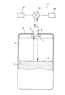
Figure 1 shows a schematic of a refinement of the
device according to the invention. A filling material 2
is stored in a container 4. The filling level meter 1,
which is mounted in an opening 6 in the lid 5 of the
container 4, serves to determine the filling level.
Measuring signals, in particular microwaves, generated
in the signal-generating unit 8 are radiated in the
direction of the surface 3 of the filling material 2
via the antenna 7. The measuring signals are partially
reflected as echo signals at the surface 3. These echo
signals are received in the receiving/evaluating unit
10 and evaluated by means of a propagation time method.
The correct timing of the dispatch of the measuring
signals and reception of the echo signals is performed
via the transmitting/receiving switch 11.
Figure 2 shows an exploded representation of the
individual layers from which the antenna 7 is assembled
in accordance with the preferred refinement. The
antenna 7 comprises a first dielectric layer 12, a
second dielectric layer 13 and a likewise dielectric
protective layer 14. A cutout 15 for holding the input
coupling unit 9 (not represented separately in
Figure 2) is provided centrally in the first dielectric
layer 12. The second dielectric layer 13 bears an
antenna structure 16, which is represented only in
part, on the side facing the first dielectric layer 12.
The second dielectric layer 13 is provided with a
conductive coating 17 on the side facing the protective
layer 14. The conductive coating 17 has radially
arranged slot-shaped openings 18 which filter the
CA 02316497 2000-08-15
- 9 - EH 369 CA
July 10, 2000
preferred propagation mode from the measuring signals
which are supplied by the signal generating unit 8. The
individual layers 12, 13, 14, from which the displayed
embodiment of the antenna 7 according to the invention
is assembled, are held together, for example, via a
bonded connection.
Figure 3 shows a section through a preferred refinement
of the input coupling unit 9 according to the
invention, via which the measuring signals are fed onto
the antenna 7. An enlarged representation of the detail
marked with A in Figure 3 is shown in Figure 3a. It is
clear from the section shown in Figure 3c that the
conductive coating 17 with the slot-shaped openings 18
over the antenna housing 30 and the flange 21 is at
frame potential.
As in the case of the previously described embodiment,
the antenna 7 is assembled from the first dielectric
layer 12, the second dielectric layer 13 and the
protective layer 14. The side, facing the first
dielectric layer 12, of the second dielectric layer 13
bears the antenna structure 16; the conductive coating
17 with the openings 18 is arranged on the opposite
side of the second dielectric layer 13. Also indicated
is the flange 21, via which the conductive coating 17
is at frame potential.
If an overvoltage occurs on the antenna structure 16,
discharging onto the conductive coating 17 takes place
through the dielectric layer 13. A discharge in the
upper section of the antenna 7 is ruled out, since the
coax cable 31 guiding the measuring signals is
insulated electrically from the conductive parts of the
antenna housing as a consequence of the glass bushing
29.
In the case shown, the input coupling unit 9 is a
radio-frequency connector, preferably an SMA connector.
CA 02316497 2000-08-15
- 10 - EH 369 CA
July 10, 2000
The contact pin for the inner conductor 22 makes
electric contact with the antenna structure 16, while
the frame contact pins 19 - which are usually four
contact pins 19 - are inserted into the blind bores 20.
The blind bores 20, which usually pass at least through
the second dielectric layer 13 and the conductive
coating 17 and terminate on or within the dielectric
protective layer 14 are provided with a conductive
inner coating 21. The frame contact pins 19 ensure that
the diversion of the overvoltages from the antenna
structure 16 can be performed in a redundant fashion.
The connection of the contact pins 19 to the conductive
coating 17, and the connection of the contact pin for
the inner conductor 22 with the antenna structure 16
are preferably performed by means of a reflow method,
as already mentioned at a previous juncture.
Figure 3b shows in addition an alternative refinement
to the radio-frequency connector 9 shown in Figure 3b.
An electrically conducting material (~ contacts 19) is
arranged in the blind bores 20 and connected to the
contact pins 19 via conductor tracks 32. The electric
contact, for example via the already previously
mentioned reflow method, is made here in the immediate
vicinity or on the surface of the second dielectric
layer 13 or on the surface of the antenna structure 16.
Figure 4 shows a schematic of the adapter 25 which
renders it possible to adapt a standard antenna 7 of a
prescribed size to a wave tube 27, which basically has
any desired dimensions. In particular, the preferred
mode can be continuously widened to any desired
diameter of the wave tube 27.
Openings 26 are provided in the lateral surface of the
adapter 25 in the border region between the adapter 25
and wave tube 27. In the case shown, the openings are
of slot-shaped configuration. In principle, however,
they can have any desired form. Whereas the openings 26
CA 02316497 2000-08-15
- 11 - EH 369 CA
July 10, 2000
suppress modes whose wall currents are oriented
perpendicular to the direction of propagation of the
measurement signals, they do not disturb the preferred
TE01 mode. These can also continue to propagate without
restriction, since the wall currents move around the
openings 26. Consequently, the adapter 25 according to
the invention also permits the use of an antenna 7
which generates and radiates any desired mode.
CA 02316497 2000-08-15
- 12 - EH 369 CA
July 10, 2000
List of reference numerals
1 Device according to the invention
2 Filling material
3 Surface of the filling material
4 Container
5 Lid
6 Opening
7 Antenna
8 Signal-generating unit
9 Input coupling unit
10 Receiving/evaluating circuit
11 Transmitting/receiving switch
12 First dielectric layer
13 Second dielectric layer
14 Dielectric protective layer
15 Cutout
16 Antenna structure
17 Conductive coating
18 Opening
19 Contact/frame-contact pin
20 Blind bore
21 Inner coating
22 Inner conductor
23 Flange
24 Connecting line/coax cable
25 Adapter
26 Opening in adapter
27 Second waveguide
28 Dielectric material
29 Glass bushing
30 Antenna housing
31 Coax cable
32 Conductor track