Note : Les descriptions sont présentées dans la langue officielle dans laquelle elles ont été soumises.
CA 02319395 2006-08-23
A FED CRT HAVING VARIOUS CONTROL AND FOCUSING ELECTRODES
ALONG WITH HORIZONTAL AND VERTICAL DEFLECTORS
TECHNICAL FIELD
The present invention relates in general to displays and in particular, to
field emission
displays.
BACKGROUND INFORMATION
The current standard for flat panel display performance is the active matrix
liquid
crystal display (LCD). However, field emission display (FED) technology has
the potential to
unseat the LCD, primarily because of its lower cost of manufacturing.
Field emission displays are based on the emission of electrons from cold
cathodes and
the cathodoluminescent generation of light to produce video images similar to
a cathode ray
tube (CRT). A field emission display is an emissive display similar to a CRT
in many ways.
The major difference is the type and number of electron emitters. The electron
guns in a CRT
produce electrons by thermionic emission from a cathode (see FIGURE 1). CRTs
have one or
several electron guns depending on the configuration of the electron scanning
system. The
extracted electrons are focused by the electron gun and while the electrons
are accelerated
towards the viewing screen, electromagnetic deflection coils are used to scan
the electron
beam across the phosphor coated faceplate. This requires a large distance
between the
deflection coils and faceplate. The larger the CRT viewing area, the greater
the depth
required to scan the beam.
FIGURE 2 illustrates a typical FED having a plurality of electron emitters or
cathodes 202 associated with each pixel on the viewing screen 201. This
eliminates the need
for the electromagnetic deflection coils for steering the individual electron
beams. As a
result, an FED is much thinner than a CRT. Furthermore, because of the
placement of the
emitters in an addressable matrix, an FED does not suffer from traditional non-
linearity and
pin cushion effects associated with a CRT.
Nevertheless, FEDs also suffer from disadvantages inherent in the matrix
addressable
design used to implement the FED design. FEDs require many electron emitting
cathodes
which are matrix addressed and must all be very uniform and of a very high
density in
location. Essentially there is a need for an individual field emitter for each
and every pixel
within a desired display. For high resolution and/or large displays, a very
high number of
-1-
CA 02319395 2006-08-23
such efficient cathodes is then required. To produce such a cathode structure,
extremely
complex semiconductor manufacturing processes are required to produce a high
number of
Spindt-like emitters, while the easier to manufacture flat cathodes are
difficult to produce with
high densities.
Therefore, there is a need in the art for an improved FED.
SUMMARY OF THE INVENTION
The present invention addresses some of the problems associated with matrix
addressable FEDs by reducing the number of cathodes, or field emitters,
through the use of
beam forming and deflection techniques as similarly used in CRTs. Because
fewer cathodes
are required, the cathode structure will be easier to fabricate. With the use
of beam forming
and deflection, a high number of cathodes is not required. Furthermore, beam
forming and
deflection techniques alleviate the requirement that the field emission from
the cathode
structure be of a high density. Moreover, within any one particular cathode,
as field emission
sites decay, the display will remain operable since other field emission sites
within the
particular cathode will continue to provide the requisite electron beam.
A plurality of cathodes will comprise a cathode structure. For each cathode,
an
electron beam focusing and deflection structure will focus electrons emitted
from each
cathode and provide a deflection function similar to that utilized within a
CRT. A particular
cathode will be able to scan a plurality of pixels on the display screen.
Software will be
utilized to eliminate the overlapping of the beams so that the images produced
by each of the
cathodes combine to form the overall image on the display.
Any type of field emission cathode may be utilized, including thin films,
Spindt
devices, flat cathodes, edge emitters, surface conduction electron emitters,
etc.
In accordance with one aspect of the present invention there is provided a
field
emission display comprising: a substrate; first, second, third and fourth cold
cathodes
deposited over the substrate, wherein the first, second, third and fourth cold
cathodes are
positioned relative to each other in an x,y matrix; one or more first
electrodes for producing a
first electric field to transition the first cold cathode from a non-emitting
state to an emitting
state to produce a first emission of electrons from the first cold cathode;
one or more second
electrodes for producing a second electric field to transition the second cold
cathode from a
non-emitting state to an emitting state to produce a second emission of
electrons from the
second cold cathode; one or more third electrodes for producing a third
electric field to
-2-
CA 02319395 2006-08-23
transition the third cold cathode from a non-emitting state to an emitting
state to produce a
third emission of electrons from the third cold cathode; one or more fourth
electrodes for
producing a fourth electric field to transition the fourth cold cathode from a
non-emitting state
to an emitting state to produce a fourth emission of electrons from the fourth
cold cathode;
first electronic optics for creating a first electron beam from the first
emission of electrons;
second electronic optics for creating a second electron beam from the second
emission of
electrons; third electronic optics for creating a third electron beam from the
third emission of
electrons; fourth electronic optics for creating a fourth electron beam from
the fourth
emission of electrons; a display screen positioned a distance from the
substrate, wherein the
display screen further comprises first, second, third and fourth partitions,
each partition
having a plurality of pixels, wherein each pixel is comprised of red, green,
and blue
sub-pixels; one or more first scanning electrodes for scanning the first
electron beam from
the first cold cathode to each of the plurality of pixels in the first
partition; one or more
second scanning electrodes for scanning the second electron beam from the
second cold
cathode to each of the plurality of pixels in the second partition; one or
more third scanning
electrodes for scanning the third electron beam from the third cold cathode to
each of the
plurality of pixels in the third partition; and one or more fourth scanning
electrodes for
scanning the fourth electron beam from the fourth cold cathode to each of the
plurality of
pixels in the fourth partition.
The foregoing has outlined rather broadly the features and technical
advantages of the
present invention in order that the detailed description of the invention that
follows may be
better understood. Additional features and advantages of the invention will be
described
hereinafter which form the subject of the claims of the invention.
BRIEF DESCRIPTION OF THE DRAWINGS
For a more complete understanding of the present invention, and the advantages
thereof, reference is now made to the following descriptions taken in
conjunction with the
accompanying drawings, in which:
-2a-
CA 02319395 2000-07-28
WO 99/39361 PCT/US99/01841
FIGURE 1 illustrates a prior art CRT;
FIGURE 2 illustrates a prior art FED;
FIGURE 3 illustrates a concept of using FEDs with beam deflection;
FIGURE 4 illustrates a side view of a display configured in accordance with
the present
invention;
FIGURE 5 illustrates a front view of a display configured in accordance with
the present
invention;
FIGURE 6 illustrates a sectional view of one cathode in the display of the
present
invention;
FIGURE 7 illustrates a detailed block diagram of a display adapter in
accordance with
the present invention;
FIGURE 8 illustrates a data processing system configured in accordance with
the present
invention;
FIGURE 9 illustrates a side view of one embodiment of the present invention;
and
FIGURE 10 illustrates an exploded view of the embodiment illustrated in FIGURE
9.
DETAILED DESCRIPTION
In the following description, numerous specific details are set forth to
provide a thorough
understanding of the present invention. However, it will be obvious to those
skilled in the art
that the present invention may be practiced without such specific details. In
other instances,
well-known circuits have been shown in block diagram form in order not to
obscure the present
invention in unnecessary detail. For the most part, details concerning timing
considerations and
the like have been omitted inasmuch as such details are not necessary to
obtain a complete
understanding of the present invention and are within the skills of persons of
ordinary skill in the
relevant art.
Refer now to the drawings wherein depicted elements are not necessarily shown
to scale
and wherein like or similar elements are designated by the same reference
numeral through the
several views.
The present invention combines the technology and advantages associated
therewith of
FEDs with beam generation and deflection of CRT technology. Though the present
invention
does not utilize a separate cathode for generating an image on each and every
pixel within the
-3-
CA 02319395 2000-07-28
WO 99139361 PCT/US99/01841
display, there are a plurality of cathodes used to generate images on a
plurality of pixels by
generating and deflecting a beam of electrons generated by a plurality of
cathodes. Essentially,
the more cathodes utilized, the flatter the display can be. This can be seen
by referring to
FIGURE 3 where a plurality of cathodes 305 each generate a beam of electrons
302, which are
deflected by an electron beam deflecting, or focusing, apparatus 303. With
this apparatus, a
plurality of pixels on display screen 301 can be illuminated by one electron
beam 302. The area
of pixels on display screen 301 that could be covered with one electron beam
302 is represented
by the cone labeled 304.
FED technology is utilized to generate the electron beams because of the
various
advantages discussed above. The use of FEDs has many advantages over the use
of thermionic
field emission from a heated cathode. Such use of thermionic emission has been
disclosed in
U.S. Patent No. 5,436,530. However, heated cathodes represent a power loss in
the system when
compared with the use of field emission. The filaments used to heat the
cathodes are delicate in
nature (fine wires must be used in order to minimize the power required),
which are prone to
vibration and sagging. Vibration and sagging are typically solved by adding
springs and by
carefully controlling the detailed shape of the filaments. However, this
entails further
manufacturing steps and costs and results in a less reliable device.
Furthermore, thermal effects
resulting from the proximity of the hot filament will cause expansion of
various parts of the
structure, which will result in changes in the electrical characteristics of
the display. Also, use
of a cold cathode permits the structure to be partially or wholly manufactured
as an integrated
device.
FIGURE 4 illustrates display 400 where images are generated on display screen
401 by
beam generation and deflection from an FED source 402. The deflection, or
focusing, of the
various electron beams is performed by beam deflection apparatus 403. The
plurality of
cones 404 represent the areas on display screen 401 illuminated by each of the
generated electron
beams. The electron beams generate images by exciting phosphors on display
screen 401. The
displayed images may be monochrome or in color.
FIGURE 5 illustrates a front view of display screen 401. Each area of display
screen 401
labeled as 501 represents an image generated by one cathode and its associated
electron
deflection apparatus. Special software will be utilized to eliminate
overlapping of the beams
between areas 501 so that the boundaries represented with dashed lines are
invisible to the
-4-
CA 02319395 2000-07-28
WO 99/39361 PCT/US99/01841
viewer. Such software is not discussed in detail in this application, since it
is not important to
an understanding of present invention.
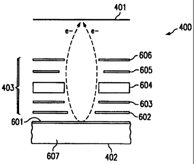
FIGURE 6 illustrates a cross-sectional view of one cathode 402 and its
associated
electron focusing and deflection apparatus within display device 400. On
substrate 607 a
cathode 601 is produced. Such a cathode 601 may comprise micro-tips, edge
emission cathodes,
negative electron affinity cathodes, diamond and diamond-like carbon films, or
surface
conduction electron emitters.
Extraction grid 602 operates to extract electrons from cathode 601 as a result
of the
difference in potential between extraction grid 602 and cathode 601.
Control grid 603 operates to modulate the electron beam current, which will,
in turn,
modulate the light output.
The electronic optics used to focus the electron beam is shown as 604;
however, this may
be comprised of a plurality of grids having various potentials applied
thereto. Such a plurality
of grids is further detailed in FIGURES 9 and 10.
Horizontal deflecting grid 605 and vertical deflecting grid 606 operate in a
similar manner
as electromagnetic deflection coils in a CRT to scan the electron beam onto
the individual pixels
on display screen 401.
One embodiment of the present invention is shown in FIGURES 9 and 10, which
illustrate one cathode assembly 900 operable for generating a plurality of
electron beams 910 for
scanning a plurality of viewing areas 501 on a display screen 401. Shown are
electron beams 910
generated on cathode 601. These electron beams are shown with dashed lines.
Note that another
four electron beams are generated from cathode 601, but these electron beams
are not illustrated
with dashed lines for reasons of clarity. Furthermore, FIGURES 9 and 10 do not
illustrate the
spacer elements used to separate the various electrodes and deflectors from
each other and from
cathode 601. Such spacer elements may be comprised of insulative materials.
Pressure plate 1004 is coupled to substrate carrier 902. Pressure plate is
used to provide
a medium by which all of the various elements of cathode structure 900 may be
connected
together, such as through the use of pressure clips. Cathode substrate 901 is
positioned on
substrate carrier 902 and held in place by clips 905. Spacers 1005 are
utilized to provide spacing
between several of the various electrodes and deflectors. Further description
of pressure
plate 1004 and spacers 1005 is not necessary for an understanding of the
present invention.
-5-
CA 02319395 2000-07-28
WO 99/39361 PCT/US99/01841
Connection wires 904 provide electric potential to cathode 601 from connecting
leads 903, which pass through insulators 906 to the underside of cathode
structure 900.
Electron emitting sites are generated on cathode 601 to generate electrons,
which are then
controlled and focused through the various electrodes, anodes, and deflectors
further described
below. Note that certain techniques may be utilized to localize the emission
sites on specific
portions of cathode 601.
As described above, extraction grid 602 assists in extracting electrons from
cathode 601,
which are passed through holes formed in extraction grid 602. Control grids
603 further assist
in the controlling of the electron beams.
The electron focusing apparatus may be comprised of first and second anodes
1003 and
1001 and focus electrode 1002, which may each have their own biasing
potentials applied
thereto. The electron beams are then passed through the gaps in horizontal
deflector 605 and
vertical deflector 606, which operate to scan the electron beams in a
controlled manner onto
display screen 401.
As an alternative embodiment, some or all of the structure illustrated in
FIGURES 6, 9
and 10 may be implemented as a monolithic structure using typical deposition,
etching, etc.
microelectronics manufacturing techniques.
Referring next to FIGURE 8, there is illustrated data processing system 800
for assisting
in the operation of a display 400 in accordance with the present invention.
Workstation 800, in accordance with the subject invention, includes central
processing
unit (CPU) 810, such as a conventional microprocessor, and a number of other
units
interconnected via system bus 812. Workstation 813 includes random access
memory
(RAM) 814, read only memory (ROM) 816, and input/output (I/O) adapter 818 for
connecting
peripheral devices such as disk units 820 and tape drives 840 to bus 812, user
interface
adapter 822 for connecting keyboard 824, mouse 826, speaker 828, microphone
832, and/or other
user interface devices such as a touch screen device (not shown) to bus 812,
communication
adapter 834 for connecting workstation 813 to a data processing network, and
display
adapter 700 for connecting bus 812 to display device 400. CPU 810 may include
other circuitry
not shown herein, which will include circuitry commonly found within a
microprocessor, e.g.,
execution unit, bus interface unit, arithmetic logic unit, etc. CPU 810 may
also reside on a single
integrated circuit.
-6-
CA 02319395 2000-07-28
WO 99/39361 PCT/US99/01841
Referring next to FIGURE 7, there is illustrated further detail of display
adapter 700.
Microcontroller 701, will utilize a state machine, hardware, and/or software
to operate the
plurality of cathodes 400 in order to produce images on display areas 501 on
display 400. A
portion of electronics 702 will be utilized for biasing the focus electrodes
604. Horizontal and
vertical deflection electrodes 606 and 605 will be controlled by blocks 703
and 704, respectively.
Cathode driver 705 will operate the various cathodes 601, while control of
control grids 603 will
be performed by control grid driver 706.
Controller 701 will operate to generate the various images on areas 501 in a
manner so
that there is no apparent boundary between areas 501, and so that areas 501
operate to generate,
either a plurality of separate images 501, or a composite image on the entire
display 401. Note
that any combination of composite images may be displayed on display screen
401 as a function
of display areas 501.
Although the present invention and its advantages have been described in
detail, it should
be understood that various changes, substitutions and alterations can be made
herein without
departing from the spirit and scope of the invention as defined by the
appended claims.
-7-