Note : Les descriptions sont présentées dans la langue officielle dans laquelle elles ont été soumises.
CA 02324123 2000-10-24
PHOTO-SENSOR CIRCUIT
BACKGROUND OF THE INVENTION
The present invention relates to a photo-sensor
circuit for detecting a light signal and converting the
detected light signal into an electric signal and, more
specifically, to a photo-sensor circuit having a shutter
function.
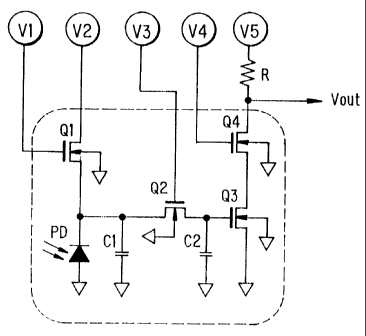
Figure 1 shows a photo-sensor circuit having a
shutter function (sample-and-hold function), which can
be used as one of pixel detecting elements composing an
image sensor. This photo-sensor circuit comprises a
photodiode PD for detecting a light signal and converting
it into an electric signal, a MOS transistor Ql for
charging/discharging a capacitor Cl being a parasitic
capacitance of the photodiode, a capacitor C2 for
accumulating a terminal voltage of the photodiode PD as
a pixel signal, a MOS transistor Q2 for transferring an
electric charge from the capacitor Cl to the capacitor
C2, a MOS transistor Q3 for amplifying a terminal voltage
of the capacitor C2 and a MOS transistor Q4 for
selectively outputting an amplified pixel signal.
The above conventional photo-sensor circuit works
with signals generated by respective parts at respective
timings as shown in Fig. 9.
Namely, a transistor Ql is turned ON when a driving
voltage Vl increases to a high level at timing tl-t2 to
1
CA 02324123 2000-10-24
give an electric charge to the capacitor Cl being a
parasitic capacitance of the photodiode PD. Once the
photodiode Pd is illuminated, a sensor current flows
causing the capacitor Cl to reduce the electric charge
by an amount proportional to the flowing current.
The transistor Q2 is then turned ON at timing t3-t4
to transfer an electric charge from the capacitor Cl to
the capacitor C2. When the transistor Q4 is then turned
ON at timing t4-t5, a current from a power supply V5 is
supplied being limited by the transistor Q3.
Consequently, a pixel signal Vout is output through a
resistance.
In this photo-sensor circuit, the transistor Q2
becomes turned-off at timing t4 and the capacitor C2
maintains a constant electric charge until the
transistor Q2 is turned OFF to transfer the electric
charge from the capacitor Cl to the capacitor C2. In other
words, during the turned-off period of the transistor
Q2 (a holding time of the capacitor C2 ), the same output
can be obtained as a pixel signal independent of a change
in the terminal voltage Vcl of the capacitor Cl.
Owing to the above-described structure, the photo-
-sensor circuit can act as a shutter for a single pixel.
The open time of this shutter can be controlled.
Figure 10 shows another structure of the photo-sensor
circuit having a shutter function, wherein a MOS
2
CA 02324123 2000-10-24
transistor is further provided for charging and
discharging the capacitor C2.
The operation of the thus constructed photo-sensor
circuit differs from that of the fore-mentioned
photo-sensor circuit by the fact that its pixel signal
is initialized by discharging the capacitor C2 when the
transistor Q5 of the circuit is turned ON at timing t6-t7
as shown in Fig. 11.
The photo-sensor circuit shown in Fig. 1 can transfer
a terminal voltage Vcl of the capacitor Cl to a capacitor
C2 by the action of the transistor Q2 and can retain the
electric charge on the capacitor C2 until the transistor
Q2 is turned ON again. Consequently, in case there is
a difference between the terminal voltages Vcl and Vc2
of the capacitors Cl and C2, the terminal voltage Vcl
of the capacitor Cl is not correctly reflected on that
of the capacitor c2 until the transistor Q is turned ON
again. This results in decreasing the reproducibility
of the signal.
Figure 12 shows a model of accumulation of electric
charge in the capacitors Cl and C2 respectively while
the photo-sensor circuit is continuously sensing light
signals.
In the photo-sensor circuit constructed as shown in
Fig. 10, the capacitor C2 can be charged and discharged
by the transistor Q5 and hence the terminal voltage Vcl
3
CA 02324123 2000-10-24
of the capacitor Cl can be well-reproducibly transferred
to the capacitor C2. However, there arises such a problem
that a signal of the capacitor C2 becomes smaller than
a signal of the capacitor Cl.
Figure 13 shows a model of accumulation of electric
charge in the capacitors Cl and C2 respectively.
SUMMARY OF THE INVENTION
Accordingly, it is an object of the present invention
to provide a photo-sensor circuit capable of
initializing a capacitor C2 by turning on a transistor
Q2 before turning ON transistor Q2 for charging and
discharging a capac.itor Cl being a parasitic capacitance
of a photodiode PD in. order to prevent the capacitor 2
from reproducing an incorrect voltage.
Another object of the present invention is to provide
a photo-sensor circuit wherein a terminal voltage Vcl
of a capacitor Cl is always applied to a capacitor C2
by turning ON a sample-and-hold transistor Q2 during the
open-state period of an shutter in order to prevent the
capacitor C2 from dropping its voltage.
A further object of the present invention is to
provide a photo-sensor circuit that can generate a pixel
signal in a wide dynamic range with high reproducibility,
which is achieved by using an initial setting means for
executing the logarithmic operation by changing a power
supply voltage V2 in addition to a shutter function.
4
CA 02324123 2000-10-24
BRIEF DESCRIPTION OF THE DRAWINGS
Figure 1 is a circuit diagram of a photo-sensor
circuit according to an embodiment of the present
invention.
Figure 2 is a time chart of signals of respective
portions of the photo-sensor circuit of Fig. 1.
Figure 3 is a circuit diagram of a photo-sensor
circuit according to another embodiment of the present
invention.
Figure 4 is a time chart of signals of respective
portions of the photo-sensor circuit of Fig. 3.
Figure 5 is an.exemplary block diagram of an image
sensor constructed of a two-dimensional matrix of
photo-sensor circuits according to the present invention,
wherein each photo-sensor circuit serves for a single
pixel.
Figure 6 is a time chart of signals generated by
respective portions of the image sensor of Fig. 5.
Figure 7 is another exemplary block diagram of an
image sensor constructed of a two-dimensional matrix of
photo-sensor circuits according to the present invention,
wherein each photo-sensor circuit serves for a single
pixel.
Figure 8 is a time chart of signals generated by
respective portions of the image sensor of Fig. 7.
Figure 9 is a time chart of signals generated by
CA 02324123 2000-10-24
respective portions of the photo-sensor circuit shown
in Fig. 1 when the circuit is operated according to a
conventional method.
Figure 10 is a circuit diagram of a conventional
photo-sensor circuit having a shutter function.
Figure 11 is a time chart of signals generated by
respective portions of the conventional photo-sensor
circuit of Fig. 10.
Figure 12 shows a model of accumulation of electric
charge in capacitors Cl and C2 respectively when the
photo-sensor circuit of Fig. 1 is operated by a
conventional metho.d.
Figure 13 shows a model of accumulation of electric
charge in capacitors Cl and C2 respectively when the
photo-sensor circuit of Fig. 10 is operated by a
conventional method.
DESCRIPTION OF THE PREFERRED EMBODIMENTS
Referring to Fig. 1, a photo-sensor circuit according
to an embodiment of the present invention comprises a
photodiode being a light-detecting element for sensing
light and converting it into an electric signal, a MOS
transistor for charging and discharging a capacitor Cl
being a parasitic capacitance of the photodiode PD, a
capacitor for accumulating therein a terminal voltage
of the photodiode PD as a pixel signal, a MOS transistor
Q2 for transferring an electric charge of the capacitor
6
CA 02324123 2000-10-24
Cl to a capacitor C2, a MOS transistor Q3 for amplifying
a terminal voltage of the capacitor C2 and a MOS
transistor Q4 for selectively outputting the amplified
pixel signal.
In the above photo-sensor circuit according to the
present invention, an electric signal corresponding to
a light signal is obtained by applying control signals
for driving respective components of the circuit.
Namely, the transistor Ql is turned ON by increasing
a driving voltage V1 to a high level at timing tl-t2 to
give an electric charge to the capacitor Cl. When light
falls on the photodiode PD, current flows in the sensor
circuit and an electric charge proportional to the
current flowing in the sensor circuit is removed from
the capacitor Cl at timing t2-t3.
During timing tl to t3 (with the shutter being open)
the transistor Q2 is in the turned-on state and the
terminal voltages Vcl and Vc2 of the capacitors Cl and
C2 are equal to each other.
When the transistor Q2 is turned off at timing t3,
the terminal voltage Vc2 of the capacitor is held at the
same level.
When the transistor Q4 is then turned on at timing
t4-t5, a current restricted by the transistor Q3 is
supplied from the power supply V5 and hence a pixel signal
is output as an output voltage Vout through a resistance
7
CA 02324123 2000-10-24
R.
In the above photo-sensor circuit structure, an
electric charge of the capacitor C2 is retained when the
transistor Q2 is turned off at timing t3 and thereafter.
The electric charge of the capacitor C2 is maintained
at a constant value until the transistor Q2 is turned
on to begin transferring the electric charge from the
capacitor Cl to the capacitor C2. Namely, while the
transistor Q2 is off (i.e., for the holding period of
the capacitor C2), the same pixel signal can be obtained
irrespective of a change in the terminal voltage Vcl of
the capacitor Cl.
Therefore, the photo-sensor circuit having 4
transistors as shown in Fig. 1 can obtain a pixel signal
Vout having high reproducibility when it is operated
according to timing chart shown in Fig. 2.
Referring to Fig. 3, a photo-sensor circuit according
to another embodiment of the present invention will be
described below.
This embodiment uses a MOS transistor Ql' in
particular for converting a sensor current of a
photodiode PD into a detection voltage that has a
logarithmic characteristic in a weak inversed state and
includes a voltage controller 1 (an initial setting
means) that can set a drain-side source voltage V2 of
the transistor Q1' to a lower voltage value (low level)
8
CA 02324123 2000-10-24
than the normal voltage value (high level) for a
specified period of time and remove an electric charge
accumulated in a capacitor Cl being a parasitic
capacitance of the photodiode PD connected to a source
side of the transistor.
The operation of the above photo-sensor circuit will
be described below with reference to the time chart of
Fig. 4.
A supply voltage V1 is set to a detection voltage value
into which a current flowing in the transistor Qi is
converted. The voltage Vl possesses a logarithmic
characteristic in the weak inversed state with the supply
voltage V2 of the high level.
In this state, once a driving voltage V2 is decreased
to the low level at timing tl-t2, a drain-source voltage
of the transistor Ql' rises and causes the transistor
Q1' to be turned ON to remove the electric charge from
a capacitor Cl being a parasitic capacitance of the
photodiode PD.
Next, the driving voltage is changed to the high level
at timing t2 and the capacitor C1 is charged with a voltage
at which a sensor current flowing through the photodiode
PD is balanced with a current supplied from the
transistor Q1'.
Since the current flowing in the transistor Q1' has
been converted into the voltage having the logarithmic
9
CA 02324123 2000-10-24
characteristic in its weak inversed state, the terminal
voltage Vcl of the capacitor Cl represents an amount of
light incident to the photodiode PD, which has been
logarithmically transformed and outputted.
During the above period tl-t3 (with the shutter being
open) , a transistor Q2 is also in the ON-state and hence
the terminal voltage Vcl of the capacitor Cl is equal
to the terminal voltage Vc2 of the capacitor Cl.
When the transistor Q2 is turned OFF at timing t3,
the terminal voltage Vc2 of the capacitor C2 is held in
the steady state.
When a transistor Q4 is then turned ON at timing t4-t5,
a current from a power supply V5 is supplied being
restricted by the transistor Q3 and a pixel signal
through a resistance R is output as an output voltage
Vout.
In the above photo-sensor circuit structure, an
electric charge of the capacitor C2 is held when the
transistor Q2 is turned OFF at timing t3 and thereafter.
The electric charge of the capacitor C2 is maintained
at a constant value until the transistor Q2 is turned
ON to begin transferring the electric charge from the
capacitor Cl to the capacitor C2. Namely, with the
transistor Q2 being in the OFF-state (during the holding
time of the capacitor C2) , the same pixel signal is output
irrespective of a change in a terminal voltage Vcl of
CA 02324123 2000-10-24
the capacitor Cl.
Therefore, the photo-sensor circuit shown in Fig. 3
can function as a shutter that is free from the effect
of afterglow and has a wide dynamic range of its
logarithmic output during the operation according a
timing chart shown in Fig. 2.
An image sensor can be constructed of photo-sensor
circuits according to any of the embodiments of the
present invention, which circuits are arranged in one-
or two-dimensional plane to form respective
pixel-detecting components.
Figure 5 is an.exemplary image sensor structure in
which the photo-sensor circuits of Fig. 1 are arranged
to form a two-dimensional matrix of the light-sensors
each representing a single pixel therein. In Fig. 5,
numeral 2 designates a pixel-selecting circuit common
to all pixels S and numeral 3 designates a pixel-signal
selecting circuit for subsequently outputting
respective pixel signals S.
Figure 6 is a time chart for respective signals of
the above image sensor.
In this instance, respective pixels S arranged in a
matrix are scanned to read at timing t4-t5 in particular.
In each photo-sensor circuit representing one pixel S,
when the transistor Q4 is turned ON, a current from the
power supply V5, restricted by the transistor Q3, is
11
CA 02324123 2000-10-24
supplied to respective pixels and hence respective pixel
signals Vout are output through a resistance connected
to a row of pixels S in the matrix.
Therefore, the above image-sensor of four-transistor
structure can obtain pixel signals each having high
reproducibility.
Figure 7 is an exemplary image sensor structure in
which the photo-sensor circuits of Fig. 3 are arranged
to form a two-dimensional matrix of the light-sensors
each representing a single pixel therein. In Fig. 7,
numeral 1 designates a voltage controller provided
common to all pixels, numeral 2 designates a
pixel-selecting circuit common to all pixels S and
numeral 3 designates a pixel-signal selecting circuit
for subsequently outputting respective pixel signals S.
Figure 8 is a time chart for respective signals of
the above image sensor.
In this instance, respective pixels S arranged in a
matrix are scanned to read at timing t4-t5 in particular.
In time charts shown in Figs. 6 and 8, it is possible
to set an accumulating period (i.e., a shutter-opening
period with a high level supply voltage V3) elongated
to timing t4.
A photo-sensor circuit according to an embodiment of
the present invention comprises a photo-detecting
element (PD) for detecting a light signal and converting
12
CA 02324123 2003-01-16
the same signal into an electric signal, a first MOS
transistor (Q1) for charging and discharging parasitic
capacitance (Cl), a capacitor (C2) for accumulating a
terminal voltage of the photo-detecting element as a
pixel signal, a second MOS transistor (Q2) for
transferring a parasitic capacitance electric charge
from the photo-detecting element to the capacitor (C2),
a third MOS transistor (Q3) for amplifying the terminal
voltage of the capacitor and a fourth MOS transistor (Q4)
for selectively outputting an amplified pixel signal.
In the photo-sensor circuit structure, the first MOS
transistor and the second MOS transistor are turned ON
for a certain period of time before accumulation of a
pixel signal to charge and discharge the parasitic
capacitance of the photo-detecting element and the
capacitor until terminal voltages of the photo-detecting
element and the capacitor become the same, the second
MOS transistor is turned OFF and the capacitor is open
after a certain period of time of accumulation of the
pixel signal and then the fourth MOS transistor is
switched ON. The photo-sensor circuit offers an
advantageous feature of producing a pixel signal having
high reproducibility.
A photo-sensor circuit according to another
embodiment of the present invention comprises a
photo-detecting element (PD) for sensing a light-signal
13
CA 02324123 2003-01-16
and converting said signal into an electric signal, a
first MOS transistor (Q1' ) for converting a current of
the photo-detecting element into a voltage having a
logarithmic characteristic in a weakly inverted state,
an initial setting means for controlling an electric
charge accumulated in the parasitic capacitance (Cl) of
the photo-detecting element connected to a source by
setting a drain voltage of the first 'MOS transistor to
a low voltage for a certain period of time, a capacitor
(C2) for accumulating a terminal voltage of the photo-
-detecting element as a pixel signal, a second MOS
transistor (Q2) for transferring a parasitic capacitance
charge from the photo-detecting element to the capacitor
(C2), a third MOS transistor (Q3) for amplifying the
terminal voltage of the capacitor and a fourth MOS
transistor (Q4) for selectively outputting an amplified
pixel signal. In this photo-sensor circuit structure,
the second MOS transistor is switched ON and at the same
time a voltage of the initial setting means is set to
a low level to bring a parasitic capacitance of the
photo-detecting element and a terminal voltage of the
capacitor into a low level state before accumulation of
a pixel signal, then after a certain period of time, the
voltage of the initial setting means is switched to a
high level state to start accumulation of a pixel signal,
then after a certain period of time, the second MOS
14
CA 02324123 2000-10-24
transistor is turned OFF to cause the capacitor to be
open, and finally the fourth MOS transistor is switched
ON. The above photo-sensor circuit offers such an
advantage that 'it can form a shutter that is free from
the effect of afterglow and has a wide dynamic range of
a logarithmic output, assuring obtaining a pixel signal
having high reproducibility.