Note : Les descriptions sont présentées dans la langue officielle dans laquelle elles ont été soumises.
' CA 02328756 2000-12-19
Doc. No. 10-425 CA Patent
Control Mechanism For Optical Cross-Connect Switches
Field of the Invention
The present invention relates to a control mechanism for optical cross-connect
switches,
particularly for optical cross- connects using tiltable mirrors for detecting
and correcting
error in mirror positioning.
Background of the Invention
IO
One of the major challenges of designing an optical cross-connect (OXC )
switch using
tiltable MEMS mirrors consists in controlling accurately each of the
individual mirrors so
that low fiber-to-fiber losses can be maintained over the operation lifetime
of the switch.
Optical matrix switches are commonly used in communications systems for
transmitting
voice, video and data signals. Generally, optical matrix switches include
multiple input
and/or output ports and have the ability to connect, for purposes of signal
transfer, any
input port/output port combination, and preferably, for N x M switching
applications, to
allow for multiple connections at one time. At each port, optical signals are
transmitted
and/or received via an end of an optical waveguide. The waveguide ends of the
input and
output ports are optically connected across a switch interface. In this
regard, for
example, the input and output waveguide ends can be physically located on
opposite
sides of a switch interface for direct or folded optical pathway communication
therebetween, in side-by-side matrices on the same physical side of a switch
interface
facing a mirror, or they can be interspersed in a single matrix arrangement
facing a
mirror.
In the OXC in accordance with the present invention the optical path between
an input
port and an output port involves the use of one or more moveable mirrors
interposed
between the input and output ports. The input and output waveguide ends remain
stationary and the mirrors are used for switching. The mirrors can allow for
two-
CA 02328756 2000-12-19
DI 106
dimensional targeting to optically connect any of the input port fibers to any
of the output
port fibers.
The major obstacle to creating an optical switch is the necessary control for
precisely
addressing each of the mirrors to achieve accurate switching with low loss.
Small errors
in angle over the optical path length of the switch result in large coupling
errors.
An optical cross-connect switch is proposed by Herzel Laor in US patent number
6,097,860, issued to Astarte Fiber Networks, Inc., for directing a beam of
light from a
fiber focused to a fixed mirror and reflected to an array of moveable mirrors.
Laor
discloses a complex control system for detecting angle deviation. Because the
optical
path includes a first and a second reflection (in a Z pattern) between
launching a focused
beam and coupling a switched beam to a selected output, a cumulative error
will be
detected at the output. To determine the angle error of each mirror is complex
and
difficult.
Further to make multiple passes between moveable mirrors increases the
complexity of
determining the angular position error of each mirror.
An accurate sensing and control system for an optical cross-connect system
employing
multiple path changes by moveable mirrors is needed.
Summary of the Invention
The present invention has found that by providing an element having optical
power in an
optical path between a first and a second moveable mirror, and a pair of
wavefront
sensors for sensing an output in a first direction and a second direction
along the optical
path, that an angle deviation from the optical path can be detected for each
of the first and
second moveable mirrors simultaneously and independently.
Accordingly, the present invention provides an optical cross-connect switch
comprising
at least one input for launching a signal;
2
CA 02328756 2000-12-19
DI 106
a plurality of outputs for selectively receiving the signal from the at least
one input via an
optical path;
a first array of independently moveable mirrors in the optical path for
redirecting the
signal from the at least one input to a second array of independently moveable
mirrors,
said second array of independently moveable mirrors for redirecting the signal
to the
selected output;
an element having optical power in the optical path between the first and
second array of
moveable mirrors;
a first wavefront sensor for detecting an angle of the signal received from
the second
array of moveable mirrors; and
a second wavefront sensor for detecting an angle of a second signal received
from the
first array of moveable mirrors launched in an opposite direction on a
substantially same
optical path from the selected output to a same at least one input.
Advantageously, each wavefront sensor can detect an angle deviation error of
one mirror.
Each mirror of each array can be checked and corrected. Using a simultaneous
control
signal, this can be done in real time.
Brief Description of Figures
Fig. 1 is an example of a preferred optical cross-connect switch;
Fig. 2 illustrates a first embodiment of a control in accordance with the
present invention
for the switch of Fig. 1;
Fig. 3 illustrates a second embodiment of a control in accordance with the
present
invention for the switch of Fig. 1;
Fig. 4 illustrates the isolation of error for a first mirror on an optical
path from left to
right, and for a second mirror on an optical path from right to left, both
optical paths
beginning from the ideal path and experiencing deviation at the mirrors;
Detailed Description of Preferred Embodiments
An example of an optical cross-connect switch for use in the present invention
is shown
in Fig. 1 Fig. 1 shows a large optical cross-connect arrangement 1200 in
accordance with
the present invention. Optical switch 1200 is scalable to 4000x4000 and is
based on
3
CA 02328756 2000-12-19
DI 106
arrays of two-dimensional tilt mirrors 1210 and 1220 and ATO lens 1230. An
input fiber
bundle 1240 is shown on the left hand side of Fig. 12. An input micro-lens
array 1250 is
placed at an end face of the input fiber bundle L240 having one micro-lens
centered on an
optical axis of each fiber. An input relay lens 1260 is provided between the
micro-lens
array 1250 and a first MEMS chip 1210 having an array of two-dimensional tilt
mirrors/micro mirrors. The distance between the input micro-lens array 1250
and the
input relay lens 1260 and the input relay lens 1260 and the first MEMS chip
1210
corresponds to a focal length of the input relay lens 1260. This input relay
lens 1260
sends a beam of light incident thereon through a hole 1270 in the first MEMS
chip 1210.
The first MEMS chip 1210 is followed by an ATO lens 1230, i.e. an element
having
optical power whose focal length corresponds to the near zone length (multi
mode) or
Rayleigh range (single mode) of the beam incident on the 2D tilt mirrors, and
a second
MEMS chip array 1220 having an array of two-dimensional tilt mirrors/micro
mirrors
and a hole 1280 disposed thereon. Both, the first MEMS chip 1210 and the
second
MEMS chip 1220 are arranged at a distance from the ATO lens 1230 which
corresponds
to the focal length of ATO lens 1230. The second MEMS chip 1220 is followed by
an
output relay lens 1290 which focuses the light to an output micro-lens array
1300
provided at an end face of an output fiber bundle 1310 having one micro-lens
centered on
an optical axis of each fiber. The distance between the second MEMS chip 1220
and the
output relay lens 1290 and the output relay lens 1290 and the output micro-
lens array
corresponds to a focal length of the output relay lens 1290. All components
are arranged
along an optical axis OA. Such an arrangement provides for an even more
compact
design of an optical switch in accordance with the present invention, and
lessens
aberration effects of the lens. In order to demonstrate more clearly how
optical switch
1200 functions, an exemplary beam of light L is traced along an optical path A
to H
through switch 1200. The beam L exits an input fiber at point A at an end face
thereof
having a miro-lens disposed thereon. The beam L propagates parallel to the
optical axis
OA until it reaches point B on the input relay lens 1260. Input relay lens
1260 sends
beam L at an angle to the optical axis OA to point C on the ATO lens 1230
through the
hole 1270 in the first MEMS chip 1210. The ATO lens 1230 sends beam L parallel
to the
optical axis OA to point D on one of the micro-mirrors on the second MEMS chip
1220.
The mirror on the second MEMS chip 1220 switches beam L to point E on one of
the
4
CA 02328756 2000-12-19
DI 106
micro-mirrors on the first MEMS chip 1210 after passing through the ATO lens
1230.
The micro-mirror on the first MEMS chip 1210 sends the light back to point F
on the
ATO lens 1230 parallel to the optical axis OA and then at an angle to the
optical axis OA
to point G through hole 1280 in the second MEMS chip 1220. The output relay
lens
1290 collects the beam of light L coming from hole 1280 in the second MEMS
chip 1220
and images it on the output micro-lens array 1300. An output fiber in the
output fiber
bundle 1310 collects beam L from the output micro-lens array 1300. It is
apparent that
this switch also functions in reverse, i.e. the output fiber bundle then
functions as the
input fiber bundle and so forth.
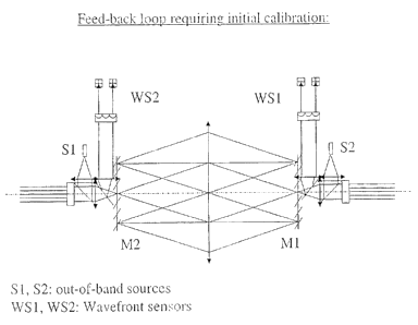
First embodiement:
This invention which builds on a previously disclosed OXC design, the in-line
ATOM
(shown in Fig. 1), proposes an optical architecture and control scheme (shown
schematically in Fig. 2) that addresses this challenge.
As seen in Fig. 2, the internal alignment of the switch core (i.e.
independently of the input
and output fiber array) is performed using two optical sources (S 1 and S2),
one
copropagating and the other one counterpropagating with respect to the input
fiber light.
The beam area of these monitoring optical sources has been expended to cover a
size
similar to that of the input/ouput fiber bundle to eliminate the need of two
additional
collimated fiber arrays (another possible option but more complex and
expensive). A hole
plate could be inserted in the path to create a beamlet array if flat
illumination is not
appropriate. The wavelengths of the two optical sources are selected in a
region outside
the intended operating range of the switch so that monitoring is concurrent
with the live
traffic. Each collimated beam is combined colinearly with the input/output
using a WDM
beam combiner. Light from the co- and counterpropagating beams is detected at
each end
using a wavefront sensor. Due to the imaging property of the switch, there is
a one to one
correspondence between every MEMS mirror inside the switch and each wavefront
sensor pixel. Consequently, light originating from S 1 which is reflected from
the MEMS
arrays, M1 then M2, gets imaged on the output wavefront sensor WS 1 and light
originating from S2 which is reflected from M2 then M1 gets imaged at the
input
5
CA 02328756 2000-12-19
DI 106
wavefront sensor WS2. This arrangement provides a unique wavefront sensor
pixel for
every individual MEMS mirror.
Typical wavefront sensor would consist in an array of microlenses coupled to
an array of
quadrant detectors. Quadrant detection will generate four electrical signals,
which will
correspond to a particular mirror orientation. These signals can be processed
to generate
an error signal and through a feedback loop move the MEMS mirror (left, right,
up and
down for example) to a predetermined position.
Although it is intended for the two monitoring optical sources to be very
closely aligned
to the input and output fiber array, small imperfections in the array
fabrication will lead
to slight misalignment between the light emerging or incident on the fiber
array (signal
light) and the sources S 1 and S2. This misalignment can be taken care in an
initial
calibration of the feed-back mechanism of the switch where every connection
would be
established, the mirror position optimized for maximum throughput and the data
(four
voltage values for a quadrant detector) stored in a look up table. The
misalignment
between the signal and S1/S2 will lead to the alignment beam being off center
on the
quadrant detectors. This situation will be taken care in the feedback
electronics through
an offset voltage setting.
Over time there could be an independent movement between the input/output
fiber array
and the monitoring optical sources, S1 and S2. This relative motion would
introduce an
increase in the OXC insertion loss if not corrected. We propose to use several
probe
beams, for example one emerging from each corner in the input fiber array,
which will
make an end to end point connection to a similar set of fibers on the output
array. The
probe beams would be kept in a closed feedback loop for optimum transmission.
Any
differential movement between the input/output fiber array, the collimating
lenses, the
MEMS mirrors and ATO lens will create a shift between the initial quadrant
detector
alignment readings and the new ones (created from the tracking loop of the
probe beams).
Using signal processing, an appropriate correction could be applied to the
initial
calibration connectivity table, which would be periodically updated using data
from the
6
CA 02328756 2000-12-19
DI 106
probe beams. This method will ensure low transmission loss assuming the
individual
input fibers are not moving independently of each other.
Second embodiement:
In an other embodiement, shown in Figure 3, it is proposed to have out-of-band
pilot tone
signals added to each input and output fibers. Four wavefront sensors are
disposed before
and after the switch core and receive light reflected from wavelength
sensitive beam
sputters (that partially reflects pilot tone light, and let the real traffic
wavelength pass
through unaffected). This is either a unique component or the association of a
beam
sputter and a filter.
Pilot tones travelling from left to right split on the first beam sputter.
Part of the light is
hitting the wavefront sensor WS3, and the other part of the pilot light
travels through the
switch. Part of this light then hits the wavefront sensor WS4. Pilot tones
travelling from
right to left split on the second beam sputter. Part of the light hits WS l,
and the rest
travels through the switch. It then splits on the first beam sputter and part
of this light hits
WS2.
The detected wavefront from WS3 and WS 1 are then the target for WS2 and WS4
respectively. Any deviation from this target would cause angular misalignment
of the
beam in front of the micro-collimators, therefore adding insertion losses.
Therefore, the
feed-back signal is the difference between the wavefront reading of WS3-WS2
and WS 1-
WS4. With wavefront sensors consisting of a microlens array and an array of
quadrant
detectors, 2 signed errors signals are obtained per wavefront sensor. The 2
error signals
from WS3-WS2 are fed back to control micro-mirrors M1, while the 2 error
signals from
WSl-WS4 are fed-back to control micro-mirrors M2. There is a unique and fixed
reliationship between the pixel on the wavefront sensors and the corresponding
micromirrors. This enables to have constant feed-back loops established.
The advantage of this embodiement is that there is no calibration of the feed-
back
mechanism required. Indeed, ideal fiber coupling corresponds to a wavefront
measured
7
CA 02328756 2000-12-19
DI 106
on WS2 being identical to the one obtained on WS3 and respectively for WS4 and
WS1.
There is no teaching of the switch required.
When the switch is assembled, its look-up table is loaded with initial value
defined
assuming ideal ATO imaging (ie linear angle per port assignement). When the 4
wavefront sensors are turned on, they immediately provide the real target for
switch
alignement, regardless of the siwtch state. Feed-back signals are used to
correct the
switch look-up table in a converging manner. An initial scan could be
performed to
guarantee that all states have been updated, but it may not be necessary since
this control
mechanism provides with both the error signal and a permanently recalibrated
target.
This control mechanism is actually providing with initial set-up, real time
calibration and
feed-back mechanism at the same time.
Wavefront sensor design (both schemes):
Since the beams impinging on the MEMS micro-mirrors are relatively big, they
are
significantly more sensitive to angular misalignment than to lateral
misalignment. This is
also true for the beams coming from the first microlens/fiber array assembly.
As an example, the beam generated by the fiber bundle+microlens array that we
plan to
use has a radius of 66.6 microns. The tolerance for 1dB of extra loss is: +/-
32 microns,
which is very loose, compared to +/- 0.2° for the angle.
To be able to sense this angular misalignement, it is proposed to use a
wavefront sensor
consisting in a microlens array with focal length of 8 mm on a pitch of 250
microns
coupled to a quadrant detector scheme also on a 250 microns pitch (ie each
detector of
the quad could be approx. 100x100 microns2).
The displacement of the beam on the quad is +/- 28 microns, with a beam
diameter (3w)
of 178 microns. It is therefore pretty easy to detect, while keeping the beam
inside its
own cell (3w + 2 displ. = 234 microns < pitch).
8
CA 02328756 2000-12-19
DI 106
The microlenses to be used are very easy to fabricate since their F# is 32.
They can be
made using refractive or diffractive lenses.
Miscellaneous:
If the microcollimator arrays are perfect, all light travelling through the
switch depicted
in Fig. 1 have to pass through the optical via-holes in the MEMS arrays.
Therefore, this
information could be used as a multiplexed error signal. This would provide
only a
warning signal as opposed to a real feed-back signal, indicating that the
switch has drifted
and that calibration is required. For example, one could have taps comparing
optical
power entering the switch to the light passing through a pin-hole similar to
the via-hole in
the MEMS arrays. Similarly, an optical fiber could be used as a pin-hole. Real
traffic or
pilot tones could be used, either added on each fibers or added in the free
space region of
the beams.
9
. . . _ ,~ , ~..~ . , . ..,. , ... . ~ 02328756 2000-12-19
.yl-
1 ~ w1~
w z '~ ~-_
T ~ ~w
t.
,1" ~~/ f"r ~ ~~ C ~ L
~.3 CAW '1
i
t
. ~ 02328756 2000-12-19 .... .,
.~ T
~,,~ 1. ~.r S ~
wz _ _, _
J
... _~
~J Z- ~. a a-.--.-. 4: ~", .l ~
t-> .~.. s~- W Wl
,", wiL -~c o c ~ ~'- ~"~ n
___-. _~~~ _ ,
_,, -.-___~ ...._....
~,-..-d~
~:. ,(...1. ~
o---
~5~1
,, ,~" t, . ".; ~ f . -e..~' ~ ~ c-~--~ - '""'-''
.-. ~,1~ w 2 -~.a .e"... e-- ~: ~... P.e. d.~ ~ ~ ~ ~l-
L'-~ o~ W S L
~. ~,...~ . ~ ~.~.~-d ~- ~-e-.-.~-v~ Yl 1
o..-o~ ,~--
~;~ <l 2 ~ ~~.~:-~ ~.: Y,.t.l -_ a ~-~.-.. ~...~ c.~... s.=-. ~ : ..... Q.,..
._ 4; .~...~ 7
>t
wS ~i. ~
,".
nz
w .
_ , J 1,., F '; :L: L : - ,
CA 02328756 2000-12-19
G-~ ~ G-~ -
_.. :~.~..
- , _ J.
_ _
~> _
~n
vm 2 ~ wS ~.
b~ ~~ ~ ~ ~~ .
ta.