Note : Les descriptions sont présentées dans la langue officielle dans laquelle elles ont été soumises.
CA 02330268 2001-O1-OS
' 9201/OS2CA
FIBER OPTIC ERRORLESS SWITCHING SYSTEM
RELATED APPLICATIONS
Not applicable
s
FEDERALLY SPONSORED RESEARCH OR DEVELOPMENT
Not applicable
MICROFICHE APPENDIX
to Not applicable
BACKGROUND OF THE INVENTION
1. FIELD OF THE INVENTION
The invention is related to the field of fiber optic communication systems,
and in
is particular, to fiber optic systems that provide errorless switching.
2. DESCRIPTION OF THE PRIOR ART
FIG. 1 depicts the current system of switching used in fiber optic networks. A
first node 101 connects to a second node 102 via a first optical fiber 150 and
a second
20 optical fiber 160. The second node 102 is comprised of a first optical-to-
electrical
converter 120, a second optical-to-electrical converter 121, a first fault
detector 130, a
second fault detector 131, and a switching system 140. The first optical-to-
electrical
converter 120 connects to the first node 101 via the first optical fiber 150.
The first
optical-to-electrical converter 120 connects to the first fault detector 130
via electrical
2s data line 151. The first fault detector 130 connects to the switching
system 140 via
electrical data line 153 and electrical control line 152.
The second optical-to-electrical converter 121 connects to the first node 101
via
the second optical fiber 160. The second optical-to-electrical converter 121
connects to
the second fault detector 131 via electrical data line 161. The second fault
detector 131
3o connects to the switching system 140 via electrical data line 163 and
electrical control
line 162.
1
CA 02330268 2001-O1-OS
9201/052CA
In operation, the first node 101 transmits a first data signal over the first
optical
fiber 150. The first optical-to-electrical converter 120 receives the first
data signal and
converts it from an optical signal to an electrical signal. The first optical-
to-electrical
converter 120 transfers the first data signal to the first fault detector 130
via electrical
s data line 151. The first fault detector 130 determines if an error has
occurred in the
transmission of the first data signal and generates a first error instruction
if an error has
occurred. The first fault detector 130 transfers the first data signal to the
switching
system 140 via electrical data line 153. The first fault detector 130
transfers any first
error instructions to the switching system 140 via electrical control line
152.
to The first node 101 transmits a second data signal over the second optical
fiber
160. The second optical-to-electrical converter 121 receives the second data
signal and
converts it from an optical signal to an electrical signal. The second optical-
to-electrical
converter 121 transfers the second data signal to the second fault detector
131 via
electrical data line 161. The second fault detector 131 determines if an error
has
is occurred in the transmission of the second data signal and generates a
second error
instruction if an error has occurred. The second fault detector 131 transfers
the second
data signal to the switching system 140 via electrical data line 163. The
second fault
detector 131 transfers any second error instructions to the switching system
140 via
electrical control line 162.
2o The switching system 140 receives the first data signal, the second data
signal,
and any first or second error instructions. The switching system 140 transfers
either the
first data signal or the second data signal. The signal that gets transferred
depends on
the first error instruction and the second error instruction. For example, if
an error
occurs on the first data signal, the first error instruction instructs the
switching system
2s 140 to transfer the second data signal and not the first data signal. If an
error occurs on
the second data signal, the second error instruction instructs the switching
system 140
to transfer the first data signal and not the second data signal.
Two problems exist with the system in FIG. 1. One problem is that duplicate
data can be transferred in the switching process. For example, consider the
situation
3o where the second data signal lags behind the first data signal. The lag in
the second
data signal causes the signals to be mis-aligned at the switching system 140.
Assume
2
CA 02330268 2001-O1-OS
9201/052CA
for this example that the second data signal lags the first data signal by ten
blocks of
data. When the switching system 140 changes from transferring the first data
signal to
transferring the second data signal, those ten blocks of data have already
been
transferred on the first data signal. After the switching system 140, the ten
blocks of
s data will again be transferred on the second data signal. The amount of
duplicated data
depends on how far the second data signal lagged behind the first data signal.
Another problem is that data can be lost in the switching process. Consider
the
other situation where the first data signal lags behind the second data
signal. The lag in
the first data signal causes the data to be mis-aligned at the switching
system 140.
to Assume for this example that the first data signal lags the second data
signal by ten
blocks of data. When the switching system 140 changes from transferring the
first data
signal to transferring the second data signal, ten blocks of data will have
been missed.
The amount of data lost depends on how far the first data signal lags behind
the second
data signal.
is Errorless switching exists in other communications networks such as
microwave
communication networks, but doesn't exist in fiber optic systems. Fiber optic
communication networks traditionally utilize Synchronous Optical Network
(SONET)
rings to provide two transmission paths to switch between. These fiber optic
communication networks do not provide for errorless switching. By today's
standards,
2o switching resulting in duplicate or lost data is not acceptable.
SUMMARY OF THE SOLUTION
The invention helps to solve the above problems by aligning the first data
signal
with the second data signal in the optic node before switching occurs. Data is
2s advantageously not lost or duplicated in the switching process.
One aspect of the invention includes an errorless switching system that is
comprised of a first fault detector, a second fault detector, a
synchronization system,
and a switching system. The synchronization system aligns the first data
signal with the
second data signal. The fault detectors detect errors in the data signals and
instruct the
3o switching system to transfer the first data signal or the second data
signal to avoid
3
CA 02330268 2001-O1-OS
9201/OS2CA
transferring erroneous data. Lost or duplicated data can be avoided by
aligning the
data signals at the switching system.
BRIEF DESCRIPTION OF THE DRAWINGS
s FIG. 1 is prior art and is an example of a switching network in a fiber
optic
system.
FIG. 2 is an example of the invention showing a switching network in a fiber
optic
system that provides errorless switching.
FIG. 3 is an example of two data signals being mis-aligned as they enter an
optic
to node and then becoming aligned before reaching a switching system.
FIG. 4 is an example of two data signals being mis-aligned as they enter an
optic
node and then becoming aligned before reaching a switching system.
DETAILED DESCRIPTION OF THE PREFERRED EMBODIMENT
is System Conficturation and Operation -- FIGS. 2 - 4
FIG. 2 depicts a specific example of an errorless switching network in accord
with
the present invention. Those skilled in the art will appreciate numerous
variations from
this example that do not depart from the scope of the invention. Those skilled
in the art
will also appreciate that various features could be combined to form multiple
variations
20 of the invention.
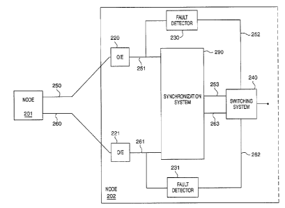
FIG. 2 shows a first node 201 connected to a second node 202 via a first
optical
fiber 250 and a second optical fiber 260. The second node 202 is comprised of
a first
optical-to-electrical converter 220, a second optical-to-electrical converter
221, a first
fault detector 230, a second fault detector 231, a synchronization system 290,
and a
2s switching system 240. The first node 201 connects to the first optical-to-
electrical
converter 220 via the first optical fiber 250. The first optical-to-electrical
converter 220
connects to the first fault detector 230 and the synchronization system 290
via electrical
data line 251. The first fault detector 230 connects to the switching system
240 via
electrical control line 252. The synchronization system 290 connects to the
switching
3o system 240 via electrical data line 253.
4
CA 02330268 2001-O1-OS
9201/OS2CA
The first node 201 connects to the second optical-to-electrical converter 221
via
the second optical fiber 260. The second optical-to-electrical converter 221
connects to
the second fault detector 231 and the synchronization system 290 via
electrical data line
261. The second fault detector 231 connects to the switching system 240 via
electrical
s control line 262. The synchronization system 290 connects to the switching
system 240
via electrical data line 263.
Those skilled in the art will appreciate that the switching system 240 is any
electronic switch, optical switch, transistor, circuit, processor, buffer,
memory controller,
gate array, or any other device or method for transferring one of two, or
more, data
to signals when commanded. Likewise, the synchronization system 290 is any
system
that can align two or more signals.
In operation, the first node 201 transmits a first data signal over the first
optical
fiber 250. The first node 201 also transmits a second data signal over the
second
optical fiber 260. The first data signal and the second data signal are
typically
is unaligned. The first optical-to-electrical converter 220 receives the first
data signal and
converts it from an optical signal to an electrical signal. The first optical-
to-electrical
converter 220 transfers the first data signal to the first fault detector 230
and the
synchronization system 290 via electrical data line 251. The first fault
detector 230
determines if an error has occurred in the transmission of the first data
signal, and
2o generates a first error instruction if an error has occurred. The first
fault detector 230
transfers any first error instructions to the switching system 240 via
electrical control line
252. The synchronization system 290 receives and aligns the first data signal
and the
second data signal. The synchronization system 290 transfers the first data
signal to
the switching system 240 via electrical data line 253 and the second data
signal via
2s electrical data line 263.
As stated above, the first node 201 sends the second data signal over the
second optical fiber 260. The second optical-to-electrical converter 221
receives the
second data signal and converts it from an optical signal to an electrical
signal. The
second optical-to-electrical converter 221 transfers the second data signal to
the second
3o fault detector 231 and the synchronization system 290 via electrical data
line 261. The
second fault detector 231 determines if an error has occurred in the
transmission of the
CA 02330268 2001-O1-OS
9201/052CA
second data signal, and generates a second error instruction if an error has
occurred.
The second fault detector 231 transfers any second error instructions to the
switching
system 240 via electrical control line 262.
FIG. 3 shows a data-level view of the system in FIG. 2 in operation. The first
s data signal, shown in the form of blocks of data, travels on electrical data
line 251 from
the optical-to-electrical converter 220 to the synchronization system 290. The
second
data signal, shown in the form of blocks of data, travels on electrical data
line 261 from
the optical-to-electrical converter 221 to the synchronization system 290.
Each
sequential number 1 - 14 in FIG. 3 represents a block of data. The first data
signal is
to the same as the second data signal except for an error 310 in the first
data signal. The
signals are mis-aligned with the second data signal lagging behind the first
data signal
when they enter the synchronization system 290. The synchronization system 290
aligns the first data signal and the second data signal before the signals
reach the
switching system 240.
is The first data signal contains the error 310. If the data signals remained
unaligned, switching from first data signal to second data signal to avoid the
error 310
would result in duplicate data being transferred. A later switch back to the
first data
signal from the second data signal would result in a loss of data. With the
data signals
aligned by the synchronization system 290, switching from the first data
signal to the
2o second data signal to avoid the error 310 does not result in duplicate or
lost data.
FIG. 4 represents the same concept as FIG. 3 except the first data signal lags
behind the second data signal. The first data signal contains the error 310.
If the data
signals remained unaligned, switching from the first data signal to the second
data
signal to avoid transferring the error 310 would result in data being lost. A
later switch
2s back to the first data signal from the second data signal would result in
duplicate data
being transferred. With the data signals aligned by the synchronization system
290,
switching from the first data signal to the second data signal to avoid the
error 310 does
not result in duplicate or lost data.
Those skilled in the art will appreciate variations of the above-described
3o embodiments that fall within the scope of the invention. As a result, the
invention is not
6
CA 02330268 2001-O1-OS
92011052CA
limited to the specific examples and illustrations discussed above, but only
by the
following claims and their equivalents.
7