Note : Les descriptions sont présentées dans la langue officielle dans laquelle elles ont été soumises.
CA 02334822 2000-12-12
WO 99/66635 PCT/GB99/01667
1
QSCILLATOR CIRCUIT
The present iLnvention relates to an oscillator
circuit, and more particularly to a tunable microwave
oscillator and to motion detectors which utilise such
oscillators.
Typically, an electronically tunable microwave
oscillator can utilise a reverse biased varactor having
a capacitance which varies according to a corresponding
variation in an applied reverse modulation voltage. In
order to effect a change in varactor capacitance, and
hence to utilise the varactor as a practical frequency
tuning device, a modulating sigõn-al of high magnitude is
required. Typically, at a frequency of oscillation of
about 10GHz, a variation of 30V in the applied reverse
modulating voltage brings about a corresponding
variation of about :ZOMHz in the frequency of oscillation
of a tunable microwave oscillator utilising such a
varactor. The frequency range over which the frequency
of oscillation of a tunable microwave varactor
oscillator can be varied is governed, in part, by the
degree of capacitarice change of the varactor over the
range over which the modulating voltage is varied. A
varactor oscillator is illustrated and described in
"Dielectric Resonators" published by Artech House and in
CA 02334822 2000-12-12
31-08-2000 63 009901667
2
GB2307355A. The relationship between the degree of
frequency modulation and applied modulating signal is
only linear for varactors over a narrow percentage
bandwidth of up to 3%. Further, relatively large
reverse biasing voltages are required for varactor
oscillators in order to realise sufficient Q to
establish and sustain oscillation. A typical biasing
voltage is of the order of 20v to 30v. At these
voltages the tuning range available is very limited..
The above renders th.e use of varactors undesirable for
low noise oscillators.
"Voltage Controller Dielectric Resonator Oscillator
Using Three-Terminal MESFET Varactor", Electronic
Letters, vol 30, no. 16, 4 August 1994, page 1320/1321,
XP000468811 ISSN: 0013-5194 discloses a voltage
controlled dielectric resonator oscillator having a
resonant circuit that is electromagnetically coupled to
a dielectric resonator thereby forming a pair of
mutually coupled resonant circuits. By varying the
MESFET varactor capacitance with a bias voltage, the
resonant frequency of the dielectric resonator can be
tuned.
It is an object of the present invention to at
least mitigate some of the problems associated wi=th
AMENDED SHEET
CA 02334822 2000-12-12
31-08-2000 GB 009901667
2a
prior art tunable microwave oscillators, preferably, f'or
use in motion detectors.
Accordingly, the present invention provides an
oscillator circuit comprising first and second mutually
electro-magnetically couplable resonant circuits, the
second resonant circuit comprising a dielectric element
and excitation means operable to produce a first
frequency of oscillation, the first resonant circuit
comprising the dielectric element and excitation means,
including a Schottky diode operable in a forward bias
mode, responsive to an applied signal, to vary the
resonant
AMENDED SHEET
- - -CA 02334822 2000-12-12
3
frequency of the first resonant circuit"-and thereby va-ry
the first frequency of oscillation of the oscillator
circuit.
Operating the Schottky diode in forward bias mode
produces a relative:ly large variation in frequency in
response to a relative small variation in modulati_ng
voltage. Furthermore, the voltages required to operate
a Schottky based oscillator are significantly less than
those required to operate a varactor based oscillator.
Preferably, an embodiment of the present inventi.on
provides an oscillator circuit wherein the modes of
resonance have associated coupling points on the
excitation means anci the excitation means is arranged
such that the coupling points are a substantially
constant distance from the dielectric element.
A further embodiment of the invention provides an
oscillator circuit wherein the dielectric element
AMENDED SHEET
-..CA 02334822 2000-12-12
D 2 9~1
comprises an arcuate profile and said 'excitation means
is arranged to follow substantially the arcuate profile
of the dielectric element.
Preferably, the excitation means comprises
excitation strip lines or microstrip lines.
Embodiments of the present invention will now be
described, by way of example only, with reference to the
accompanying drawings in which:
figure 1 illustrates schematically a typ ical
transmit-receive arrangement of a motion detector;
figure 2 shows schematically a prior art oscillator
for a motion detection device;
figure 3 depicts schematically an oscillator for a
motion detection device according to an embodiment;
figure 4 illustrates the antenna patches of a
microwave detector;
figure 5 shows a ground plane having two antenna
coupling slots for the microwave detector as is also
illustrated in WO 92/09905;
AMENDED SHEET
CA 02334822 2000-12-12
WO 99/66635 PCT/GB99/01667
figure 6 depicts the microwave detector microstrip
circuitry disposed on the opposite side of the board
bearing the ground plane; and
5
figure 7 illustrates the microwave detectors
microstrip circuitry having the components disposed
thereon.
The use of trLe doppler effect for detecting motion
is well known within the art. For example, in microwave
intruder detectiori devices it is known to provide a
dielectric resonator oscillator and diode mixer, mounted
in a cavity, which are arrangeci to provide an output or
transmit signal at a required frequency and an input or
receive signal, toa3ether with a doppler IF output.
Referring to figure 1, there is shown schematically
a microwave circuit 100 having oscillator 102 producing
an output frequency fo connected to a filter 104 arranged
to pass the fundamental frequency of the oscillator, fo,
and to block the second and higher order harmonics
thereof. The output from the filter 104 is fed to a
power divider 106 to produce a transmit signal and a
local oscillator signal. A transmit antenna 108 is used
to radiate the transmit signal. The local oscillator
CA 02334822 2000-12-12
WO 99/66635 PCT/GB99/01667
6
signal 110 is fed to a mixer 112. The mixer 112 has an
input from the receive antenna 114 arranged to receive
the reflected signal. As is well appreciated within the
art if the receiveci signal was reflected from a moving
object, it will be a doppler shifted version of the
transmit signal. The mixer 112 combines the local
oscillator signal with the received signal received by a
receive antenna 114. The output 116 from the mixer :L12
contains the doppler frequency produced by the
reflection of the transmit signal of frequency fo from a
moving body (not shown). The presence or absence of the
doppler signal at the output 116 determines whether or
not a moving object has been detected.
Referring to figure 2, there is shown schematically
a prior art embodiment for a motion detector circuit
having an oscillator 102 comprising first 201 and second
202 mutually coupled resonant circuits. The first
resonant circuit 201 of the oscillator 102 arrangement
shown in figure 2:is a varactor 204 in conjunction with
a microstrip line 206 arranged to resonate close to the
frequency of operation of a dielectric resonator 208.
The second resonator circuit 202 comprises the
dielectric resonator 208 electromagnetically coupled, in
use, to a further microstrip line 210 connected to the
CA 02334822 2000-12-12
WO 99/66635 PCT/GB99/01667
7
gate of field effect transistor 214 and a microstrip
line 211 connected to the drain of field effect
transistor 214 and which forms part of the feedback loop
of the oscillator. The FET 214 utilises various
impedances which are arranged to correctly match the FET
214.
By varying or modulating the varactor capacitance
with an applied voltage 222, the resonant frequency of
resonant circuit 201, can be tuned resulting in a change
of oscillation frecpuency of the resonant circuit 202.
It will be appreciated by one skilled in the art
that the closer the electromagn~.tic coupling between the
dielectric resonator and the microstrip lines, the
greater the resultant frequency control. This increased
frequency control is at the expense of decreased
oscillator Q facto:r.
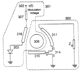
With reference to figure 3, there is shown an
oscillator circuit for a microwave detector according to
an embodiment of the present invention. The oscillator
300 comprises first 301 and second 302 mutually coupled
resonant circuits.
The first resonant tuning circuit 301 consists of a
CA 02334822 2000-12-12
WO 99/66635 PCT/GB99/01667
8
microstrip line 316 which has a Schottky diode 303
connected at one end, and a modulation voltage 322,
v(t), applied via resistor 307, to the other end of said
microstrip line. The tuning line 316 is situated
adjacent to the dielectric resonator 308 so that, in
use, the dielectric resonator 308 and the tuning line
316 are electromagnetically coupled.
Electronic frequency tuning of the oscillator 300
is achieved by varying the modulation voltage 322, which
causes the junction capacitance of the Schottky diode
303 to vary. The change in capacitance brings about a
change in the effective length of the tuning line 316
thereby altering the resonant frequency of the tuning
line 316. Since the first resonant tuning circuit 301
is mutually coupled to the second resonant circuit 302
via the dielectric resonator 308, the oscillation
frequency of the oscillator 300 also varies according to
the variation of the modulation voltage 322.
Preferably, the Schottky diode is a BAT15-03W
available from Siemens operable at a diode voltage of
close to OV. L'rnder such operating conditions the
variation in capacitance is as shown in table 1 below.
MFL CLfÃ
-0.05 241
CA 02334822 2000-12-12
WO 99/66635 PCT/GB99/01667
9
0.00 245
+0.05 252
TABLE 1
It will be appreciated that an increase in forward
voltage from OV to 0.05V brings about a 2.9% increase in
capacitance.
In the present oscillator embodiment a DC voltage
is applied to the Schottky diode 303 (connected in
forward bias) via resistor 307. Typically, the
frequency of the oscillator 300 is shifted by -12MHz
from a nominal frequency of 10.525GHz, at an applied
tuning voltage 322 of +5V. The frequency shift may be
changed by altering the coupling to the dielectric
resonator 308.
For comparison, a typical prior art varactor-tuned
oscillator operating at a frequency of 10GHz requires a
variation of up to 30V in the modulating voltage in
order to produce a frequency shift of 20MHz.
The Schottky diode 303 is operated in a forward
bias mode. This is in contrast to the varactor 204 of
figure 2 which is operated in reverse bias. The higher
CA 02334822 2000-12-12
WO 99/66635 PCT/GB99/01667
degree of change in junction capacitance of the Schottky
diode 303 at small forward voltages is capitalised on,
resulting in a relatively large change in effective
length of tuning line 316, and hence large frequency
5 shift of the oscillator 300. The complete tunable
oscillator 300 may thus be operated with voltages which
are of significantly smaller magnitude as compared to
the voltages used in conventional varactor-tuned
oscillator 102. A significant reduction in component
10 and circuit cost tY:Lus results.
Although figure 3 shows the use of a single
Schottky Diode, the present invention is not limited
thereto. It will be appreciat4o by one skilled in the
art that diodes or diode pairs could equally well be
utilised to realise an embodiment of the present
invention. Furthermore, embodiments can also be
realised in which the microstrip lines are arcuate as
opposed to being straight. Still, further it will be
appreciated that the position of the circuit elements
depicted in figure 3 et seq are not fixed and can be
suitably repositioned without departing from the scope
of the present invention. It will also be appreciated
by one skilled iri the art that there are many other
possible oscillator topologies which can be realised
using the present invention.
CA 02334822 2000-12-12
WO 99/66635 PCT/GB99/01667
11
Figure 4 shows the antenna circuit board 400 which
can be of singe-sicied construction and carries separate
transmit and receive antenna arrays. The transmit
antenna array comprises two microstrip patch elements,
406 and 408, which are interconnected and connected to a
common feed line 418. The receive antenna array a:Lso
comprises two microstrip patch elements, 402 and 404,
which are interconr.Lected and connected to a common feed
line 416. Various 2.2 mm holes B are provided to aid
the positioning of the antenna board 400 to or on a
suitable housing (not shown). Four 3 mm holes Al and A2
are provided secure the antenna board 400 to or within
the housing (not shown). A11.;Siimensions are shown in
millimetres.
Figure 5 and 6 show the groundplane 500 and the
component side circuitry 600 respectively of the
microwave board. Figure 7 shows the component side of
the microwave board 600 with the components mounted
thereon. The oscillator circuit 700 is enclosed by the
broken line. The oscillator circuit comprises a first
301 and second 302 electromagnetically couplable
resonant circuits. The first resonant circuit comprises
means for receivincl a modulating voltage v(t) including
a connection tab 702, a 1KOhm resistor 307, a forward
CA 02334822 2000-12-12
WO 99/66635 PCT/GB99/01667
12
biased Schottky diode 303 and a tuning line 316
electromagnetically couplable to the dielectric
resonator 308.
The second circuit 302 comprises the dielectric
resonator 308 coupled, via microstrip lines 310 and 311
to the gate and d:rain of a FHX35LPT transistor 314.
Power is provided to the transistor 314 via a 39 Ohm
resistor 704.
The output from the oscillator circuit 700 is fed
via a decoupling capacitor 706 to the transmit 708 and
receive 710 portions of the detector. The transmit
portion 708 comprises a microst;r
~ip line 612 for coupling
to the transmit antenna. Similarly, the receive portion
710 receives via microstrip line 610 a reflected version
of the transmitted signal. The microwave board 600 and
the antenna circuit: board 400 are mounted back-to-back
with the groundplane intervening. The alignment of the
boards is such that the transmit array feed line 418
overlies the associated feed line 612 on the microwave
board. Similarly, the receive array feed line 416 on
the antenna board overlies the associated feed line 610
on the microwave board. Coupling between the microwave
circuit board and the antenna board is achieved by the
provision of two narrow slots 502 and 504 in the
CA 02334822 2000-12-12
08-08-2000 GS. 00990 66'
13
groundplane layer of the microwave board. The reflected
signal and the output from the oscillator circuit are
combined using a mixer diode 712, for example, a BAT1.5-
099, to produce ar.i IF signal which is output via
connection tab 608.
AMENDED SHEET