Note : Les descriptions sont présentées dans la langue officielle dans laquelle elles ont été soumises.
CA 02339611 2001-02-05
WO 00/23820 , PCT/US99/23741
TITLE OF THE INVENTION
DIRECT RADIOGRAPHIC IMAGING PANEL WITH SHIELDING ELECTRODE
TECHNICAL FIELD
This invention relates to radiation detection panels comprising a plurality of
radiation sensors mounted beneath a field electrode and associated readout
electronic
I o elements outside the field electrode, and more particularly to a radiation
detection panel
which includes a shielding electrode protecting the readout electronics.
BACKGROUND OF THE INVENTION
15 Imaging radiation panels for detecting imagewise intensity modulated
radiation such
as x-ray radiation and for producing an electronic signal representing the
image in the
modulated radiation which rnay be digitized, stored, computer enhanced and
subsequently
displayed as a visible image in a number of different display media are well
known. Such
panels include an array of a plurality of sensors able to convert incident
radiation directly to
2o an electrical charge indicative of the intensity of the incident radiation.
Typically such
sensors comprise a complex structure which includes a radiation detection
element and a
charge storage element. The radiation detection element may be a photodiode
operating
together with a scintillation layer to detect photons emitted when radiation
strikes the
scintillation layer and produce a charge proportional to the photon intensity.
or it may be a
25 photoconductor which produces electrical charges directly when exposed to
radiation and a
charge collecting electrode to collect such charges. The charges so produced
are typically
stored in some storage device, most often a charge storage capacitor.
Typical such panels are described in, for example: Jeromin, U.S. Pat. No.
5,168,160; Lee,
30 U.S. Pat. No. 5.319,206; Lee, U.S. Pat. No. 5,652,430; Jeromin et al. U.S.
Patent 5,381,014,
Hughes et al. U.S. Patent x.315,101 and Tran, U.S. Patent x,254,480.
SUBSTITUTE SHEET (RULE 26)
CA 02339611 2001-02-05
WO 00/23820 PCT/US99/23741
-2-
Regardless of the particular type of sensor used, be it a photoconductor type
or a
photosensitive layer, most panels also employ a field electrode which usually
extends
uninterrupted over alI sensors to apply a biasing field to the individual
sensors. Also
regardless of the particular sensor type used, most panels include electronic
circuitry for
addressing each sensor and recovering the charge stored therein in a manner
which permits
an image reconstruction sensor by sensor, each sensor forming a picture
element or PIXEL
of the complete image. Again the most commonly elements used to address each
sensor are
MOSFET switches, and are constructed using thin film technology, thereby often
being
referred to as TFT switches.
Associated with the sensors are sensitive electronics in the form of a
plurality of
integrated circuit chips, usually integrating amplifiers which receive the
charge from the
sensors and amplify it to produce a usable electronic signal proportional to
the stored charge
generated by the incident radiation.
The amount of charge that forms the initial signal prior to amplification is
exceedingly small. The amplifiers are therefore most often placed as close as
possible to the
sensors, which in practical terms means along the panel edges right next to
the beginning of
the outermost column and line of the sensor array. As was stated previously,
in most
structures the sensor array is covered by the field electrode, which is co-
extensive with the
sensor array perimeter. Therefore the amplifiers tend to be in very close
proximity to this
field electrode. Depending on the sensor exact nature and the mode of
operating the panel, a
biasing voltage is applied to this field electrode and this biasing voltage
may be raised to
quite high levels. When this voltage is high, the amplifiers are susceptible
to current
leakage between the field electrode and the amplifier input and occasionally
to voltage
breakdown between the field electrode edge and the amplifier input leads.
Typically the
detector is enclosed in a container. The field electrode may generate ionized
air that is
confined by the container and that can drift over the amplifiers. The input
signal to the
amplifier may thus receive a noise spike or other noise signals. Such noise
spikes or signals
show on the image as a series of lines that are unacceptable to consumers of
the radiation
detection panels because the lines tend to obscure the actual image.
SUBSTITUTE SHEET tRULE 28)
CA 02339611 2001-02-05
WO 00/23820 . PCT/US99/23741
-3-
It is an object, therefore, of the present invention to provide a panel
comprising a
plurality of sensors, of the type which includes a field electrode, capable of
creating an
image that is substantially free of unacceptable noise lines.
SUMMARY OF THE INVENTION
In accordance with this invention, there is provided an image capture panel
comprising:
a substrate
a radiation detection layer over the substrate;
to
a field electrode over the radiation detection layer, the field electrode
having an
edge;
an electric ground; and
a shielding electrode extending along said edge and electrically separate
therefrom,
said shielding electrode electrically connected to said electric ground.
The radiation detector panel will typically further include an electronic
signal detection
2o element on said substrate adjacent said field electrode edge. The shielding
electrode is then
located between the signal detection element and the field electrode edge.
Also in most
embodiments of this invention, the shielding electrode also extends completely
around the
field electrode edge.
The shielding electrode is preferably biased to ground via a resistor, and may
be
constructed of a conductive paint, such as silver or graphite paint.
BRIEF DESCRIPTION OF THE DRAWINGS
The invention can be more fully understood from the following description
thereof
in connection with the accompanying drawings described as follows.
SUBSTITUTE SHEET (RULE 26)
CA 02339611 2001-02-05
WO 00/23820 _ PCT/US99/23741
-4-
Figure i is a schematic elevation of a radiation sensor used with the present
invention.
Figure 2 shows a radiation detection panel wherein the shielding electrode
extends
along one side of the field electrode only.
Figure 3 shows a cross section along arrows 3-3 of the radiation detection
panel of
figure 2 showing the shielding electrode of the present invention placed along
the
photoconductor layer side.
Figure 4 shows a schematic elevation of an alternate embodiment of this
invention
wherein the shielding electrode is placed over the top dielectric layer over
the field
electrode.
Figure ~ shows a schematic elevation of an alternate embodiment of this
invention
wherein the shielding electrode completely covers the portion of the top
dielectric layer
directly over the field electrode.
Figure 6 shows a schematic elevation of an alternate embodiment of this
invention
wherein the shielding electrode conformally covers the amplifier chip and
associated
contacts.
Figure 7 shows a schematic elevation of an alternate embodiment of this
invention
wherein the shielding electrode covers the amplifier chip and associated
contacts but has an
open end adjacent the contacts.
Figure 8 shows a radiation detection panel in accordance with the present
invention
wherein the shielding electrode extends all around the field electrode.
Figure 9 shows a radiation detection panel in accordance with the present
invention
wherein a shielding electrode extends around each amplifier and integrator
chip.
SUBSTITUTE SHEET (RULE 26)
CA 02339611 2001-02-05
WO 00/23820 . PCT/US99/23741
-5-
DETAILED DESCRIPTION OF INVENTION
The invention will next be illustrated with reference to a specific panel
which
employs sensors that convert incident x-ray radiation to an electrical charge
and store the
charge in a charge storage capacitor. Such type of sensor is described in more
detail in co-
pending application Serial Number 08/987,485 filed 12/09/97 in the names of D.
L. Y. Lee,
L. Cheung and L. Jeromin and assigned to the assignee of the present
invention, the contents
of which are incorporated herein by reference. The invention will also be
illustrated with
reference to the figures wherein similar numbers indicate the same elements in
all figures.
Such figures are intended to be illustrative rather than limiting and are
included herewith to
facilitate the explanation of the apparatus of the present invention.
Referring now to figure 1, there is shown in schematic cross section elevation
representation the internal structure of a sensor 10 according to this
invention. The sensor
10 is built on a substrate 12 which may be glass, ceramic, or other suitable
insulating
material which provides enough mechanical strength to support the layers and
circuitry
comprising the sensor.
Also shown are two conductive elements, placed adjacent each other to form a
first
or bottom conductive microplate 14, and a second, or middle, conductive
microplate I6. A
first dielectric layer I 8 is placed between the two microplates. The two
microplates and the
dielectric layer form charge-accumulating capacitor 20. The conductive
elements may be
2o thin layers of a conductive material such as indium-tin-oxide, or a thin
layer between SOA
and 1 OOA of metal.
An FET transistor 22 is also built on the substrate 12. Typically this
transistor has a
gate electrode 24, a gate oxide coating 26, and a semiconductive material 28
such as
amorphous silicon. The gate electrode is connected to a conductor extending
along the
sensor. This conductor permits access to the gate permitting addressing the
FET gate from
outside the detector to switch the FET on or off at will. The FET also
comprises a source
and a drain electrode. The source electrode 30 is connected to the second
conductive
microplate 16 and the drain electrode 32 is connected to a conductor (not
shown) leading to
a contact for connecting the sensor to a charge detector or amplifier.
SU8ST1TUTE SHEET (RULE 26)
CA 02339611 2001-02-05
WO 00/23820 PCT/US99/23741
-6-
A radiation detection layer which is typically a photoconductive layer 34, and
which
preferably exhibits very high dark resistivity, overlays the previously
deposited layers. In
radiography, particularly in medical applications, the incident radiation is X-
ray radiation,
and the radiation detection layer is an X-ray photoconductor. The
photoconductive layer
may comprise amorphous selenium, lead iodide, lead oxide, thallium bromide,
cadmium
telluride, cadmium sulfide, mercuric iodide or any other such material. It may
comprise
organic materials such as polymers that may be loaded with X-ray absorbing
compounds
that exhibit photoconductivity when the captured radiation is X-ray radiation.
In a preferred embodiment, this layer is a continuous amorphous selenium layer
300
to 500 micrometers thick.
A second dielectric layer 36 is placed over the photoconductive layer, a
conductive
field electrode 38 is placed over the second dielectric layer, and a third
dielectric layer 40 is
t5 placed over the field electrode 38. Field electrode 38 is preferably a
layer of indium-tin-
oxide; other conductive material such as chromium, aluminum, etc. may be used.
The field
electrode should be selected so that it is substantially transparent to the
radiation one wishes
to detect. When such radiation is X-ray radiation the field electrode is
preferably a
conductive layer which is highly penetrable by such radiation.
A programmable power supply 60 (shown in figure 2) is used to apply a charging
voltage to the sensor. The power supply is connected to the field electrode 38
and to the
bottom microplate 14 of the storage capacitor. Typically the bottom microplate
is connected
to an electrical common point for the circuit, usually a ground 62
In a preferred embodiment, the middle microplate 16 extends over the FET and
an
insulating layer 42, such as a SiOx layer, preferably Si02, is placed between
the middle
microplate 16 and the photoconductor layer 34.
The technology for creating the sensors is preferably vacuum deposition of
alternating layers of conductive, dielectric and insulating materials, and is
well known in
SUBSTITUTE SHEET (RULE 26)
CA 02339611 2001-02-05
WO 00/23820 _ PCT/US99/23741
_ 'j _
the art. See for instance "Modular Series on Solid State Devices" Volume 5 of
Introduction
to Microelectronics Fabrication by R. C. Jaeger, published by Addison-Wesley
in 1988.
Referring now to figures 2 - 9, there are shown a number of views illustrating
the
configuration of components in accordance with specific embodiments of the
present
invention. A plurality of sensors 10 may be arrayed on a supporting structure
50 to provide
an imaging panel capable of capturing radiation produced images, as shown in
figure 2.
Each of the sensors forms a PIXEL, or picture element. Such a panel may be
made as a
single unit or may be a composite of a plurality of smaller panels to achieve
a desired size.
The aforementioned US Patent Number 5,381,014 issued to Jeromin et al. on
October 8,
1996 discloses a technique for making larger panels using smaller units.
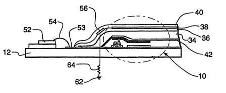
A plurality of conductors 53 (only a portion of which is illustrated) extend
between
the sensors. Each pixel 10 in a row is electrically connected to an adjacent
one of said
conductors 53 through the FET in the sensor. Each conductor 53 is in turn
connected to the
signal input pads 51 of mufti-channel amplifier 52 via contact 54, which may
be in the form
of a wire bond. A single amplifier 52 is generically shown on the side of the
panel in figure
2, but it should be understood that each amplifier may comprise a plurality of
integrated
circuit chips. According to one embodiment of this invention, a shielding
electrode 56 is
placed all along an edge 58 of the field electrode 38, between the amplifiers
52 and the field
electrode edge closest to the amplifiers. The shielding electrode 56 is
electrically insulated
from the conductors 53 and is preferably sandwiched between second dielectric
layer 36 and
the third dielectric layer 40. In cases where there are amplifiers and
corresponding leads
extending all around the perimeter of the field electrode, as shown in figure
8, the shielding
electrode 56 completely surrounds the periphery of field electrode 38.
Although the term "shielding" electrode is used throughout this description to
refer
to various embodiments, the electrode may prevent the unacceptable noise lines
on the
resulting image by one or more mechanisms that may be more properly
characterized as
shielding, guarding, or prevention. Shielding often implies providing a
barrier that
encapsulates the source and/or destination of the spurious charge, and
prevents signal
SUBSTITUTE SHEET (RULE 26)
CA 02339611 2001-02-05
WO 00/23820 , PCT/US99/23741
_g_
influence by spurious charge migration and external fields or radiation.
Guarding often
implies acting as an antenna to provide a more attractive destination for the
spurious charge
than the destination being guarded. Prevention denotes schemes that inhibit
creation of the
offending electrical influences. "Shielding electrode" is used herein
generically to refer to
the electrode of the present invention that prevents the unacceptable noise
lines by one or
more of the above mechanisms, which may or may not include shielding as
defined above.
Guards, in particular, are most effective when they are exactly, or at least
approximately, at the same potential as the signals they protect, particularly
if they are
located very near the circuitry being protected. The most sensitive portions
of circuitry
being protected in the present invention are the signal inputs (contacts 54)
for amplifiers 52,
typically biased at relatively low voltage (for example +5 volts). Because
this low voltage is
very close to ground, especially when compared to the thousands of volts
applied to some of
the nearby circuitry, it may be practical and acceptable to connect the
various shielding
15 electrode embodiments disclosed herein to ground. It may be preferable,
however, to supply
connection points, such as dedicated amplifier signal input connector pads,
biased at the
more precise amplifier reference voltage for connection of the shielding
electrode. This type
of connection is described in detail with reference to a specific embodiment,
below, but is
applicable to all the shielding electrode embodiments described herein.
The shielding electrode may be connected to a resistor. Providing resistance
in the
connecting circuitry may limit current during faults, such as sparks or flash-
over. In
addition, resistance may dampen transients, and eliminate or at least mitigate
overshoot and
ringing. The wiring materials for connecting to the shielding electrode may be
strategically
zs selected to introduce the desired resistance, thus avoiding extra
components.
Figure 3 illustrates a panel having a preferred placement of the shielding
electrode
56, which as shown is on the normally sloping side of the photoconductor
layer. The
shielding electrode is typically about 1 mm wide. To avoid excessive current
leakage
3o between the field electrode and the shielding electrode, a gap of about 1
mm is maintained
between field electrode 38 and shielding electrode 56. Shielding electrode 56
is interposed
SUBSTITUTE SHEET (RULE 26)
CA 02339611 2001-02-05
WO 00/23820 . PCT/US99/23741
-9-
between field electrode 38 and conductors 53. Thus, shielding electrode 56
captures any
current leakage whether direct or from ionized air adjacent the panel surface,
rather than
such current leakage being picked up by the amplifier and resulting in
unacceptable noise
lines on the image. In this sense, shielding electrode 56 operates both as a
guard, because it
attracts spurious charge better than the more distant signal inputs to
amplifier 52, and a
shield, because it is directly in the preferred path of surface-charge
movement.
In an alternate embodiment shown in figure 4, the shielding electrode 56' may
be
located on top of the third dielectric layer 40. When so located, shielding
electrode 56' acts
to primarily as an antenna-like guard capturing aerial (floating) spurious
charge.
In another embodiment, shown in figure 5, shielding electrode 156, rather than
being
a ring around field electrode 38, completely covers dielectric layer 40 or at
least that portion
of dielectric layer 40 directly over field electrode 3 8. In addition to
shielding and guarding
is against such current leakage, shielding electrode 156 may prevent such
current leakage by
inhibiting high-voltage external fields that influence at a distance and
generate spurious
charge. Such a shielding electrode 156 may be constructed by a vacuum
deposition process.
Rather than having a single shielding electrode over the field electrode 38,
there may
2o be a plurality of shielding electrodes 256, each completely covering an
amplifier chip 52 and
its associated contacts 54, as shown in figure 6. Such a shielding electrode
256 may be
constructed as a conformal coating over a dielectric layer 255 directly over
the chips 52 and
contacts 54, and may act both as a shield as well as a guard against substrate
surface leakage
and aerial charge.
In an alternate embodiment, shown in figure 7, shielding electrode 256' may be
a
stand-alone, box-like structure having an open end 258 adjacent contacts 54,
and may
function merely as a guarding antenna.
As shown in figure 8, shielding electrode 56 (as weal as 56', 156, 256, or
256') is
3o connected to ground 62, preferably via a resistor 64. In a preferred
embodiment, as shown
in figure 4, two resistors, 64 and 64' are used on diametrically opposing
corners of the
SUBSTITUTE SHEET (RULE 28)
CA 02339611 2001-02-05
WO 00/23820 . PGT/US99/23741
-10-
panel providing two grounding paths rather than one. Typical resistor values
are 10 kS2 to
200 kS2, but other sizes may also be adequate depending on the application,
panel structure,
and voltages involved.
Finally, in yet another alternate embodiment, as shown in figure 9, the
shielding
electrode may be in the form of a shield conductor 56" associated with
amplifier 52. In
such an embodiment, each signal conductor 53 may terminate adjacent to an
amplifier 52
signal input connector pads 51. Typically such conductors are formed using
microlithographic processes well known in the art, on supporting structure 50.
Shield
conductor 56" is electrically isolated from the signal conductors 53, and is
interposed
between the field electrode 38 edge and the paths of the signal conductors 53.
Shield
conductor 56" terminates adjacent to amplifier 52, and may thus be wirebonded
to
corresponding shield conductor input pads 51 on the amplifier as shown, for
each amplifier
52 in figure 9 in the same way as conductors 53 connected to sensors 10 are
wirebonded to
~ 5 the amplifier. The pads 51 to which shield conductor 56" is connected may
be merely
dummy pads biased at the amplifier reference voltage. This connection scheme
may be
applied to any of the various shield electrode embodiments disclosed herein.
Alternatively,
the shield conductor 56" may merely be connected directly to ground 62 or via
a resistor 64"
as shown for amplifier 52' in figure 9. Where there are a plurality of
integrated circuit
chips that make up a larger "hybrid" circuit chip, there may be a separate
shield conductor
56" for each chip or for each hybrid chip.
In a preferred embodiment, the material of the shielding electrode comprises a
conductive paint that can be applied with a syringe-type dispenser. Silver
paint has
demonstrated especially good conduction, but other conductive paints, such as
graphite
paint, may also be used. In the alternative, the shielding electrode may
comprise a thin line
of conductive paste, or may be a printed or photolithographically-formed
electrode.
More than one of the aforementioned embodiments may be used together, as
necessary. The embodiments described herein are only intended for
illustration, without
limitation. of some of the ways that the sensitive electronics of an image
capture panel can
be shielded or guarded from leakage currents. Many other embodiments of a
similar
SUBSTITUTE SHEET (RULE 26)
CA 02339611 2001-02-05
WO 00/23820 . PCT/US99/23741
-11-
nature can be envisioned, and are to be construed as being encompassed within
the scope of
the present invention.
In the particular panel embodiment used for illustrating this invention, the
panel is
first charged by applying a charging voltage between the field electrode and
the bottom
microplates. The panel is then exposed to radiation that carries image
information as a
modulated intensity. The radiation impinges on the panel for a preset
duration, and charges
proportional to the radiation intensity are generated and stored in the
storage capacitors.
Appropriate signal processing, (preferably of the type disclosed in United
States Patent
to Number 5,648,660 issued to Lee et al.) is used to recover the accumulated
charges in all of
the storage capacitors in the detectors in the panel and to reconstruct a
visible image. Any
current leaking from the field electrode, and any current due to adjacent
ionized air over the
panel, is intercepted before it reaches the amplifiers, captured and directed
to ground by the
shielding electrode.
The invention has been described in detail with reference to a particular
sensor type,
however this was done for illustration purposes and is not intended to limit
this invention to
panels having this type of sensor only. As was initially stated the shielding
electrode placed
according to this invention is applicable whenever a field electrode or top
electrode is used
in a panel which is biased in a manner which produces leakage current which
interferes with
the signal detection. The exact nature of the underlying detector is not
controlling. Those
skilled in the art having the benefit of the teachings of the present
invention as hereinabove
set forth, can effect numerous modifications thereto. These modifications are
to be
construed as being encompassed within the scope of the present invention as
set forth in the
appended claims.
SUBSTITUTE SHEET (RULE 26)