Note : Les descriptions sont présentées dans la langue officielle dans laquelle elles ont été soumises.
CA 02341166 2001-02-19
WO 00/12960 PCT/US99/19601
1
Title
Thin Film Strain Sensors Based on Interferometric Optical Measurements
Background of the Invention
1. Field of the Invention
The invention relates to polymeric/semiconductor thin film strain gauges
2. Description of the Relevant Art
Many civil engineering structures display fatigue, and occasionally failure,
after
years of exposure to natural forces. In other instances, the failure is a
result of a
catastrophic event, such as an earthquake, tornado, or hurricane. There is a
need for
1o an inexpensive, robust, and sensitive strain gage that is unaffected by
seasonal
environmental variations. Further, such a sensor should be simple, easily
installed,
and readily integrated into modern data communication systems.
The sensor system disclosed herein can monitor the integrity of structures for
the purpose of public safety and maintenance. Specific applications include
building,
road, and bridge integrity. The system employs, as the sensing component,
multiple
optical strain gages that are inexpensive, inert to natural environments, and
physically
robust. Combined with an automated data collection and diagnostic analysis
programming, such sensors and their optical fiber data links can be placed on
the
superstructures and footings of bridges, in the support components of
buildings, or
2o embedded into the surfaces of roads and pedestrian skywalks. The 'health'
of such
structures and surfaces can be automatically monitored and assessed with a
minimum of
human time allocation. Detailed use information would also be valuable in
assessing
the need for routine maintenance or for the need for repair after a potential
catastrophic
loading.
2s Summary of the Invention
The sensitivity and the passivity behavior of the sensors distinguishes from
the
prior art. Current resistive strain sensors have gage factors (the measure of
sensitivity)
of about 2-3. The disclosed sensors have gage factors on the order of 200-800.
It is
not believed the prior art discloses any passive sensors that have a memory
that does
CA 02341166 2001-02-19
WO 00/12960 PCT/US99/19601
2
not rely on a power source.
Thin films of semiconductors or polymers are used to measure strain. The thin
films are layered with each layer consisting of materials with different
refractive
indices. Because each layer has a different refractive index, light that is
introduced
into the composite structure can either be reflected or pass through at each
interface.
This allows interference of the incident light that passes through with light
that is
reflected resulting in a measurable absorption change. The degree of
interference is
sensitive to the refractive index and thickness of each layer. The thickness
of the each
layer changes with application of an external stress. The consequence of this
is that the
~o light absorption changes as a function of strain so that the absorption
change can be
used to measure the strain.
There are two types of interferometric sensors disclosed herein, active and
passive. An active sensor responds to the strain reversibly, i.e. as the
strain changes
the absorption changes in a reversible and predictable fashion. This type of
sensor is
used to measure the existing strain on a structure.
A passive sensor has a memory of the maximum strain experienced by the
structure. For example, if a structure experiences a large deformation ( a
large strain)
but then relaxes to a small rest value, the large deformation is not
reversible. An
active sensor will measure the strain events only if continuously monitored
while the
2o passive sensor will measure only the maximum strain experienced. If the
active sensor
is not being monitored while the maximum strain is occurring, the large strain
excursion will not be observed. The passive sensor overcomes this problem.
Broadly the invention comprises both active and passive sensors which
preferably are used in the same structure. Both sensors are constructed by
layering
materials, either semiconductors or polymers having different refractive
indices. The
sensitivity is increased when the difference in refractive index is maximized
and also as
the number of layers is increased. The passive sensors are constructed by
adding small
particulates to one set of layers.
Brief Description of the Drawings,
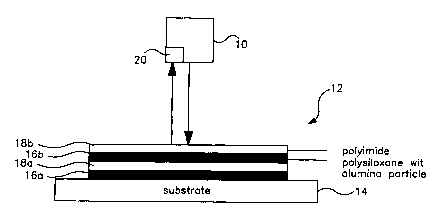
3o Fig. 1 is an illustration of a passive sensor;
Figs. 2a and 2b are illustrations of an alternative embodiment of Fig. 1;
CA 02341166 2001-02-19
WO 00/12960 PCT/US99/19601
3
Fig. 3 is a graph of the optical response of an active sensor;
Fig. 4 is a graph of the optical response of an passive sensor; and
Fig. 5 is a graph of the optical response of a passive sensor;
Description of the Preferred Embodiments)
s incident light can be measured in reflectance or transmission to determine
the
strain.
Referring to Fig. 1, reflectance mode, visible light from a spectrometer 10,
such as Perkin Elmer Lambda 2, is directed onto a thin film passive sensor
shown
generally at 12. The sensor 12 comprises a transparent glass substrate 14 and
a
laminated construction in succession from the substrate 14, of a polyimide
layer 18a, a
polysiloxane layer 16a filled with alumina particles, a polyimide layer 18b
and a
polysiloxane layer 16b filled with alumina particles. The incident light beam
is normal
to the sensor surface. The light is collected along the incidence beam path in
a
photomultiplier tube detector 20 in the spectrometer 10. The layers can range
in
thickness from 1-20 microns. The passive sensor is prepared by mixing 50 nm
particles
of aluminum oxide in with the polysiloxane layer in an amount of 0.5 to 10 %
by
weight based on the total weight of the polysiloxane layer. During
preparation, the
small particles aggregate to some (currently unknown) degree. Under strain,
some of
the particles in the aggregate separate and the polymer fills in between the
newly
2o separated alumina particles. When the strain is removed, the particles
cannot
reaggregate because of the intervening polymer. This is detected optically
because the
size of the aggregates determines the amount of light scattered off of the
sample: as the
aggregate size changes because of the strain, the amount of light directed
toward the
detector changes since the detector only samples a small volume of space. The
passive
sensor requires no power to achieve its memory effect.
Referring to Fig. 2a, the transmission mode, for an active sensor a capillary
tube 30, e.g. i.d. 0.5 mm; o.d 0.7 mm, is used as a light conduit. Thin films
32, e.g.
polysiloxane/polyimide, are deposited onto the outside walls of the capillary
tube 30
and then these filins are coated with aluminum 34. The aluminum 34 serves as a
3o mirror to keep all the light confined in the tube 30 and to protect the
entire structure
from the surrounding environment. A fiber optic source 3b inputs light in a
CA 02341166 2001-02-19
WO 00/12960 PCTNS99/19601
4
wavelength range of 500 to 1,000 Angstroms into one end of the capillary
tube 30 parallel to the longitudinal axis of the tube and a detector 38
collects the light
at the other end.
In the capillary configuration, the tube 30 acts as both a waveguide and a
sensor. Under no strain, most of the light passes down the tube without
interacting
with the walls. With application of a strain the capillary tube 30 bends, Fig.
2b, so
that a significant amount of light is introduced into the thin film coatings
along the tube
walls. Two effects cause a modulation of the output light intensity. First,
the path
length is changed so any absorption that occurs is increased, depending upon
the
1o absorptivity of the wall materials and the number of bounces the light
undergoes.
Second, the interference effect observed as light passes through the thin film
layers still
is operative, also causing intensity modulation by constructive or destructive
interference, depending on the refractive index and thickness of each layer
and the
wavelength of light used.
The film thicknesses 32 are on the order of 1 to 20 microns, thinner being a
bit
better. The wavelengths of maximum response depends upon the layer
thicknesses, but
that wavelength can be chosen arbitrarily to match the thin film structure.
The
aluminum coating has a thickness of between 400 to 800 nm.
The alternating layers must have a different refractive index and the larger
the
2o difference, the better the sensor response. Polyimide has n = 1.6-1.7
(depending upon
the exact polyimide used, the nature of the curing, and the supplier);
polysiloxane has
n=1.44. Other commonly available transparent polymers polyethylene,
polypropylene, Teflon~, polyvylidene flouride, polyester, etc. have refractive
indices
around 1.4 and could substitute for the polysiloxane layer. High refractive
index
polymers such as polycarbonates have refractive indices approximately the same
as
polyimide.
A preferred sensor system requires both a passive and an active sensor in
close
proximity. The passive sensor measures the maximum strain excursion
experienced
but not a temporal history, i.e. the measured strain may be current or
previous. Thus,
3o the role of the active sensor is to measure the existing strain at the time
of
measurement.
CA 02341166 2001-02-19
WO 00/12960 PCT/(JS99/19601
The sensors can be applied to a structure by currently known bonding
techniques used for the current generation of strain sensors. Because the
sensors are
small, they will measure the strain of the substrate material reliably. The
optical
source and detector need not be embedded with the sensor. With the appropriate
fiber
5 optic connections, the optical measurement can be made periodically by
connecting a
handheld spectrometer to the input and output of the sensor. Thus, for
example, after
an earthquake the maximum strain experienced by each structural element in a
building
could be determined well after the event (days or weeks) to establish the
safety of the
building since the passive sensor retains this information even with (the
likely) loss of
l0 power. Alternatively, a fiber optic network connected to each sensor in a
building that
remotely senses the strain automatically. However, during a catastrophic event
the
fiber network is likely to break and prevent this mode of operation.
The materials used in the sensor are both inexpensive and robust. For example,
the polysiloxane is a commercially available gasket sealer. The capillary
configuration
~s is especially attractive for long term applications because, if necessary,
the entire
sensor can be enclosed. Then, for example, if the sensor is to be used in a
harsh
environment such as a bridge, the entire sensor can be isolated from wind,
rain, salt
spray, etc. because any coatings applied outside of the aluminum layer have no
affect
on the sensor performance.
2o Examples
Examples of the sensor response are given in Figures 3, 4 and 5. The light
source was a tungsten lamp, and strain was applied by four point bending, see
ASTM
C-1341-97.
Figure 3 shows the response of two different active strain sensors, one with
12
25 layers (6 alternating layers of polysiloxane and poiyimide) and one with 26
alternating
layers. Layer thickness was about 10 microns. The absorbance was monitored at
600
nm as a function of applied strain with the results shown. The gage factor is
a function
of the number of layers indicating the interferometric nature of the response.
Further,
the gage factors are large, more than two orders of magnitude larger than
found in
3o typical resistance strain gages. Finally, the response is linear and
reversible over the
entire range up to about 2000 p,strain (this is the typical limit required for
structural
CA 02341166 2001-02-19
WO 00/12960 PGT/US99/19601
6
applications since most materials exceed their plastic deformation limits at
about
2000 pstrain).
Figure 4 shows the response of a passive strain gage having 26 alternating
layers. The layer thickness was about i0 microns. As strain is applied, the
response is
similar to an active gage. The absorbance was monitored at 600 nm. However,
when
the strain is released the response is no longer reversible, i.e., the 0-
strain absorbance
depends upon the history of the sample. This is demonstrated in Figure 4 for
several
different strain excursions. The virgin gage has an absorbance value at 600 nm
of A =
0.73. Application of 300 ,strain changes this to A = 0.83. Upon release of the
stress
~ o back to 0 pstrain the absorbance returns to A = 0.78, shown as the short
dashed line in
Figure 4. Application of any strain less than 300 ,strain follows the dashed
line path
reversibly. However, if the strain exceeds 300 pstrain, then the path reverts
to the
solid line as shown for the 600 pstrain point in Figure 4. Now when the stress
is
released, a new path is taken, shown as the dotted line, and to a new
absorbance at 0
t s pstrain.
The increments between successive strain excursions decreases with increasing
strain (i.e., the passive response is nonlinear) and this is demonstrated in
Figure 5.
The 12 layer gage has a small gage factor but a larger, nearly linear response
range.
The 26 layer gage has a larger gage factor but becomes clearly nonlinear at
2o significantly smaller maximum strains.
The foregoing description has been limited to a specific embodiment of the
invention. It will be apparent, however, that variations and modifications can
be made to
the invention, with the attainment of some or all of the advantages of the
invention.
Therefore, it is the object of the appended claims to cover all such
variations and
25 modifications as come within the true spirit and scope of the invention.
Having described our invention what we now claim is: