Note : Les descriptions sont présentées dans la langue officielle dans laquelle elles ont été soumises.
.,. ... . _ .. .~.~~~r_~~ ~~u : ~~~ _ ~ , , ~ t : 1 ~, 7 u~~.5~jt~a'._ic,- +44
f3~ Z; "
20-09-200C,j ' ' '/ ' a ° r v ~ a r ; a urr:~sn 'n i ~ r r uu . ; v-. ~
~ a r uu US 009921475
1
LOW TUMPERrITURE FORrI~IATIUN OR B~1C:KKS]Dh OHMiC
CONTACT'S FOk VER'!'fCALDrVICES
FIELD OF TFIE INVErrTlON
The present inventi an relates to ohmic contacts to semiconductor materials.
1n
particular, the invention mlates to methods of fonnixtg ohmie contacts to
devices that
include a plurality of semicaaductor materials.
BACICGROUND 4F THE INVENT1~N
In the micmeEectronics context, circuits ate made fxom the segttential
1o connection of setnicorsductor devices. Generally speaking, semicanductor
devices arc
operated by, and are used to control, the flow of electric current within
specific
circuits to accomplish particular tasks. To connect scmiconductar devices to
ane
another, apprapriatc contacts must be made between the semiconductor devices,
Hecause of their high conductivity, the most useful and convenient materials
far
carrying current from one device to another are metals,
Such metal contacts should interfere either minimally ar preferably not at all
with tl3e operation of the device or the current currying metal. Furthermore,
the metal
contact must be physically and chemically compatible with the scmiconduetnr
material to which it is attached, The types of contact that exlubit these
desired
2o characteristics are la~awn as "ohmic contacts".
An olunie contact is usually defined as a metal-semiconductor contact that has
a negligible contact resist~ce relative to the bulk or spreading resistance of
the
semiconductor, Sxe, Physics of Semiconductor Devices, Second Edition, 1981,
page
344. As further stated therein, an appropriate ahmic contact will not
significantly
zs change the performance of the device to which it is attached, and it can
supply any
required current with a voltage drop that is appropriately small compared with
the
drop across the active region of the device.
Oblate contacts and methods of producing ohmic contacts arc larown in the
art. For example, U.S. Patents 5,409,859 and 5,323,022 to Glass et al. ("Glass
3o patents"), discuss an ohmic contact structure formed of platinum and p-type
silicon
carbide and a method of making the ohutic structures. L. SpieLi et al.,
"Aluminium
Implantation ofp-SiC for Ohmic Contacts," Diaiuond and Related Materials, vol.
6,
pp, 1414-1419 (1997); r. Chen et al., "Cazstaet Resistivity ofRe, Pt and Ta
Fifms Qrt
ltl3PLACBMPNT SHEE?
CA 02343416 2001-03-09 AMENDED SHEET
.u..~...m.., w. .-v- _ _ ~~ . ~r.j ~5 ~.
~~.m
20-OG-2000' m.u: m_L:; ~~"nv:an m: i :LU, rv~r,,:v.:
<«~.YJt:.~,:.- ' US 009921475
'.
Ill
n-type B-SiC: preliminary results," Materials and Scicnce $ngineering, B29,
pp. l 85-
189 (1995); and WO 98137584 also discuss ohnnic contacts and SiC.
Although ohmic contacts and methods of making thera are lcnown, the known
methods for producing ohmic contacts, and especially
REPLACBM~N~' SHEET
AMENDED SHEET
CA 02343416 2001-03-09
WO OO/1b382 PCT/US99/21475
2
those produced using a silicon carbide substrate, are difficult even when
properly
conducted.
The problems associated with obtaining ohmic contacts are myriad and
cumulative. Limited electrical conductivity of the semiconductor due to low
hole or
electron concentrations may hinder or even prevent the formation of an ohmic
contact.
Likewise, poor hole or electron mobility within the semiconductor may hinder
or even
prevent the formation of an ohmic contact. As discussed in the Glass patents,
work
function differences between the contact metal and semiconductor may give rise
to a
potential barner resulting in a contact exhibiting rectifying (non-ohmic)
current flow
1 o versus applied voltage. Even between two identical semiconductor materials
in
intimate contact with greatly differing electron-hole concentrations, a
potential barner
(built-in potential) may exist, leading to a rectifying rather than ohmic
contact. In the
Glass patents, these problems were addressed by inserting a distinct p-type
doped SiC
layer between the p-type SiC substrate and the contact metal.
15 More difficult problems are encountered when forming ohmic contacts for
newer generation gallium and indium based semiconductor devices. The formation
of
an ohmic contact between a semiconductor and a metal requires the correct
alloying of
the semiconductor and the contact metal at their interface. Selectively
increasing the
hole/electron concentration at the semiconductor surface where the ohmic
contact
2o metal is deposited is known as an effective means for enhancing the contact
process to
achieve an ohmic contact. This process is typically achieved through ion
implantation, which is well recognized as a selective doping technique in
silicon and
silicon carbide technologies. However, in the case of silicon carbide, ion
implantation
is usually performed at elevated temperatures (typically >600 °C) in
order to
25 minimize damage to the silicon carbide crystal lattice. "Activating" the
implanted
atoms to achieve the desired high Garner concentrations often requires anneal
temperatures in excess of 1600 °C, often in a silicon over pressure.
The equipment
required for this ion implantation technique is specialized and expensive.
After the high temperature ion implant and subsequent anneal, the contact
3o metal is deposited on the implanted substrate surface and annealed at
temperatures in
excess of 900 °C. This method of forming contacts on semiconductor
devices that
CA 02343416 2001-03-09
WO 00/16382 PCTNS99/21475
incorporate gallium nitride or indium gallium nitride is not feasible because
these
compounds disassociate at elevated temperatures.
One theoretical answer to this problem would be to form an ohmic contact on
the substrate prior to growing the delicate epitaxial layers (e.g, gallium
nitride layers)
necessary to complete the semiconductor device. This approach is undesirable,
however, because it inserts an undesired contaminant, the contact metal, into
the
epitaxial growth system. The contaminant metal can effect epitaxial growth by
interfering with lattice growth, doping, rate of reaction or all of these
factors. In
addition, metal impurities can degrade the optical and electrical properties
of the
to epitaxiallayers.
Similarly, many semiconductor devices such as metal-oxide-semiconductor
field-effect transistors ("MOSFETS") require a layer of a semiconductor oxide
(e.g.
silicon dioxide). The high temperatures associated with traditional ion
implantation
techniques and implant or contact metal annealing processes place high stress
on
15 oxide layers, which can damage oxide layers, the semiconductor-oxide
interface and
the device itself. Alternatively, forming the ohmic contact prior to creating
the oxide
layer is not practical because the oxidizing environment utilized to form the
oxide
layers has adverse effects on the ohmic contact.
Accordingly, a need exists for a practical and economical method for forming
2o an ohmic contact for use in conjunction with a semiconductor device that
does not
exhibit the manufacturing problems previously discussed. The need also exists
for a
type of a semiconductor device that incorporates an ohmic contact but is
economic to
manufacture.
25 It is an object of the invention is to provide a semiconductor device that
incorporates an ohmic contact.
It is a further object of the invention to provide a semiconductor device
comprising silicon carbide and an ohmic contact.
It is a further object of the invention to provide a semiconductor device that
3o incorporates an ohmic contact that is economic to manufacture.
It is a further object of the invention to provide a method for forming a
CA 02343416 2001-03-09
WO 00/16382 PCT/US99/21475
4
semiconductor device that incorporates an ohmic contact.
The invention meets these objects with a method for forming a metal-
semiconductor ohmic contact for a semiconductor device. The method comprises
implanting a selected dopant material into a surface of a semiconductor
substrate
having an initial conductivity type. The implanted dopant provides the same
conductivity type as the semiconductor substrate. The dopant implantation is
followed by annealing the implanted semiconductor substrate a first time at a
temperature and for a time sufficient to activate the implanted dopant atoms
and
increase the effective carrier concentrations. Depositing a metal on the
implanted
surface of the semiconductor material follows the first anneal. Thereafter, an
annealing of the metal and the implanted semiconductor material occurs. This
second
anneal is at a temperature below which significant degradation of any
epitaxial layers
placed on the substrate would occur, but high enough to form an ohmic contact
between the implanted semiconductor material and the deposited metal.
~5 The invention also meets these objects with a semiconductor device
comprising a semiconductor substrate having a first surface and a second
surface and
a first conductivity type. The device also comprises at least one epitaxial
layer that is
grown or placed upon the first surface of the semiconductor substrate. The
semiconductor substrate is further defined as having a zone of increased
carrier
2o concentration in the substrate extending from the second surface (the
surface opposite
the epitaxial layer) toward the first surface. The device further comprises a
layer of
metal deposited on the second surface of the substrate to form an ohmic
contact at the
interface of the metal and the zone of increased carrier concentration.
The foregoing and other objects, advantages and features of the invention and
25 the manner in which the same are accomplished, will become more readily
apparent
upon consideration of the following detailed description of the invention
taken in
conjunction with the accompanying drawings, which illustrate exemplary
embodiments, and wherein:
30 FIG. 1 is a schematic cross-sectional diagram of a semiconductor
device according to the present invention.
CA 02343416 2001-03-09
WO 00/16382 PCT/US99/21475
FIG. 2 is a schematic cross-sectional diagram of a dopant implantation
as utilized in the method according to the invention.
The present invention is a semiconductor device incorporating an ohmic
contact and a method of forming the ohmic contact.
It will be understood by those familiar With wide bandgap semiconductors,
such as silicon carbide, and semiconductor devices formed therefrom that the
invention is most useful in making a semiconductor device and ohmic contact
utilizing n-type or p-type silicon carbide ("SiC"). Accordingly, for ease of
1o explanation, the following description ofthe invention and examples will be
directed
toward an embodiment of the invention utilizing SiC. Those skilled in the art,
however, will readily recognize that the invention may be easily adapted for
use with
other semiconductor materials such as silicon, gallium nitride, aluminum
gallium
nitride, and indium gallium nitride. As used herein, aluminum gallium nitride
and
15 indium gallium nitride include compounds where the mole percents of
aluminum and
gallium or indium and gallium equal 1.
In a broad aspect the invention is a semiconductor device comprising a
semiconductor substrate having an initial concentration of dopant imparting an
initial
conductivity type. The semiconductor substrate may be either n-type or p-type.
The
2o device also comprises at least one epitaxial layer situated adjacent one
surface of the
semiconductor substrate.
The claimed semiconductor device is further characterized in that the
semiconductor substrate is defined by a zone of increased carrier
concentration
extending from the surface of the substrate opposite the epitaxial layers
toward the
25 surface adjacent the epitaxial layers. A layer of metal is deposited on the
substrate at
the zone of increased carrier concentration to form an ohmic contact at the
interface of
the metal and the substrate.
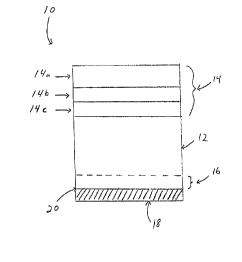
Referring now to FIG. 1, a schematic of a semiconductor device 10 according
to the invention is presented. The device 10 comprises a semiconductor
substrate 12,
3o which for purposes of explanation is considered to be SiC. It should be
understood,
however, that other semiconductor materials, such as silicon, may be used as a
CA 02343416 2001-03-09
WO 00/16382 PCT/US99/21475
6
substrate in the practice of the invention. The SiC substrate 12 may be either
p-type
or n-type.
Situated adjacent the SiC substrate 12 are the additional components 14
necessary to complete the semiconductor device. For example and as represented
in
FIG. 1, the semiconductor device may be a light emitting diode ("LED") having
sequential expitaxial layers 14a, 14b, and 14c of p-type and n-type
semiconductor
materials. In a preferred embodiment, the invention is a vertical
semiconductor
device such as a LED, metal-oxide-semiconductor field-effect transistor
("MOSFET"), lasers, or Schottky rectifiers that are comprised of several
epitaxial
to layers situated adjacent a semiconductor substrate. As will be discussed
later, the
device according to the invention is particularly suited for vertical
semiconductor
devices that comprise materials having low melting or low disassociation
temperatures. Such materials would include gallium nitride, indium gallium
nitride
and aluminum gallium nitride.
15 The claimed device is further characterized as having a zone of increased
carrier concentration 16 on the backside of the semiconductor substrate. In
other
words, the semiconductor substrate, in this case SiC, has a carrier
concentration near
the surface of the substrate opposite the epitaxial layers that is higher than
the carrier
concentration exhibited in the remainder of the substrate.
2o The line that serves as the boundary to the zone of increased Garner
concentration 16 is dotted to represent the fact that there is no sharp
boundary at
which the carrier concentration when the substrate 12 suddenly changes. The
carrier
concentration decreases as the distance from the backside surface of the
substrate
increases until the carrier concentration equals the initial carrier
concentration. As
25 will be discussed below, the zone of increased carrier concentration is
formed by a
room temperature ion implantation technique using dopants commonly associated
with p-type and n-type semiconductor materials.
For example and still refernng to FIG. 1, a preferred embodiment of the
claimed device comprises a n-type SiC substrate doped with nitrogen. It should
be
3o understood that n-type SiC formed of other n-type dopants along with the
various
types of p-type SiC also may be used in accordance with the invention. The SiC
CA 02343416 2001-03-09
WO 00/16382 PCTNS99/21475
substrate 12 is preferably slightly to highly doped and possess an initial
carrier
concentration between about 1x10¹⁵ and about 1x1019 cm-3. The terms "slightly"
and "highly" are imprecise and are purposely used to show that the initial
carrier
concentration may vary considerably. Although the initial carrier
concentration may
vary considerably, testing has shown that substrates that are initially
moderate to
highly doped provide the best results. Through ion implantation of a selected
dopant
material (e.g. nitrogen) at the surface opposite the epitaxial layers 14, a
zone 16 is
created that contains a higher Garner concentration than the remainder of the
substrate
12. Preferably, the ion implantation is conducted at a level that creates a
zone of
to increased Garner concentration 16 on the backside of the substrate that
exhibits a
carrier concentration between about 1x10'8 and about 1x10z° cm 3 and
that is always
higher than the initial carrier concentration.
Those skilled in the art will recognize that a zone of increased carrier
concentration as described previously may also be formed during the growth of
the
15 substrate. However, the difficulties associated with the variable feed
rates of the
required dopants and other difficulties typically associated with crystal
growth
methods make this approach impractical.
The preferred n-type dopants for use in forming the zone of increased carrier
concentration 16 are nitrogen, arsenic and phosphorous. Preferred p-type
dopants for
2o use in forming the zone of increased carrier concentration 16 are aluminum,
boron and
gallium.
Although Applicant does not wish to be bound by a particular theory, evidence
suggests that the zone of increased carrier concentration 16 allows for the
creation of a
metal contact that exhibits ohmic properties. In a preferred embodiment, a
selected
25 contact metal 18 having a melting point, vapor pressure and physical and
chemical
properties suitable for use with the overall semiconductor device is deposited
at the
surface of the SiC substrate at the zone of increased Garner concentration 16
to form
an interface 20 between the metal and the substrate. Preferred metals include
nickel,
palladium, platinum, aluminum and titanium with nickel being most preferred.
The
3o device, including the metal and the substrate is then annealed at a
temperature low
CA 02343416 2001-03-09
WO 00/16382 PCT/US99/21475
enough to avoid damage to the device and specifically any epitaxial layer, but
high
enough to form an ohmic contact at the interface of the metal and substrate.
Again, although the Applicant does not wish to be bound by any particular
theory, it appears useful to create the zone of increased Garner concentration
to serve
as the receptor for the contact metal. Thus, in another embodiment, the
invention
comprises the method of forming the ohmic contact utilized in the previously
described semiconductor device.
In a broad aspect, the invention is a method for forming a metal-
semiconductor contact for a semiconductor device. The method comprises
implanting
1o a selected dopant material into a semiconductor substrate having a first
conductivity
type and wherein the implanted dopant provides the same conductivity type as
the
substrate. For purposes of this discussion it will be assumed that the
semiconductor
substrate is a SiC substrate and that the dopant material is deposited into a
surface of
the SiC substrate. Those skilled in the art, however, will readily recognize
that the
15 invention may be easily adapted for use with other semiconductor materials.
An
annealing step follows the implanting of the selected dopant material. In this
annealing step the implanted SiC substrate is annealed at a temperature and
for a time
sufficient to activate the implanted dopant atoms to effectively increase the
carrier
concentration of the implanted dopant atoms in the SiC substrate. A contact
metal is
2o then deposited on the implanted surface of the SiC substrate. The deposited
contact
metal and the implanted surface of the SiC substrate are then annealed. This
second
annealing is at a temperature below that at which any expitaxial layer placed
on the
substrate would experience significant degradation but high enough to form an
ohmic
contact between the implanted SiC and the deposited metal.
25 In a preferred embodiment, the semiconductor substrate may comprise a n-
type or p-type substrate that may possess a slight, moderate, or high initial
dopant
concentration. For example, where n-type SiC is the substrate, the SiC
substrate may
possess an initial dopant concentration from about 1x10'5 (slightly doped) to
1x10'9
cm' (highly doped). The terms "slight," "moderate," and "high" are imprecise
and
3o are used to indicate that the initial concentration of dopant in the
substrate material
may vary. Testing has shown that moderate to highly doped substrates achieve
the
CA 02343416 2001-03-09
WO 00/16382 PCTNS99/21475
best results with the invention.
The semiconductor substrate is then implanted with a selected dopant material
and annealed. Preferably, the dopant implantation occurs at room temperature
and the
subsequent annealing occurs at a temperature between about 800°C and
about 1300°C.
Dopants usually associated with the conductivity type of the substrate may be
used as
the dopant for the implantation step. For example, when n-type SiC initially
doped
with nitrogen is the substrate, nitrogen may serve as the implanted dopant.
Likewise,
when p-type SiC initially doped with aluminum is the substrate, aluminum may
serve
as the implanted dopant. Other possible n-type dopants are arsenic and
phosphorous.
1 o Boron and gallium may serve as alternative p-type dopants.
Those skilled in the art will readily recognize that the implanting of the
dopant
material may be accomplished at high temperatures. In fact, high temperature
implantation is typically preferred in the SiC context in order to reduce
damage to the
SiC lattice structure. In the SiC context, however, high temperature ion
implantation
15 places constraints on the commercial use of the invention. Ion implanting
equipment
with the capability of heating the SiC substrate during implantation are
atypical,
expensive and intended for research and development rather than low cost, high
volume applications. Furthermore, when SiC substrates are heated to high
temperatures, they must be heated and cooled at a rate that will not produce
fractures
20 thereby slowing down the production process.
Accordingly, room temperature implantation is the preferred implantation
method for use in the invention. It has been discovered that room temperature
implanting of dopant followed by an annealing step in a simple vented furnace
capable of reaching 1300°C and holding 100 or more substrate wafers
achieves
25 satisfactory results and greatly increases throughput.
The room temperature implantation of dopant is preferably conducted so as to
create a zone of increased dopant concentration near the implanted surface of
the
semiconductor substrate. FIG. 2 is a schematic representation of the
implantation
process according to the invention. In this example, a n-type SiC substrate 22
having
30 an initial dopant concentration of approximately 1x10'$ cm 3 is implanted
with atomic
or diatomic nitrogen 24 at energies of 10 to 60 keV with doses of 1x10" cm 2
or more.
CA 02343416 2001-03-09
WO 00/16382 PCT/US99/21475
In some instances more than one implant energy may be used to create a more
graduated Garner concentration distribution. The implantation process produces
a
zone 26 near the implanted surface of the SiC substrate approximately 1000
angstroms in depth having a total chemical dopant concentration of
approximately
1x10'9 to 1x10²° cm 3 with the concentration of the implanted dopant
decreasing as the
distance from the implanted surface increases. The dopant concentration
outside of
the zone of increased dopant concentration 26 remains substantially the same
as the
initial dopant concentration. The boundary of the zone of increased carrier
concentration 26 is represented as a dotted line to indicate that the change
in carrier
1o concentration between the zone 26 and the remainder of the substrate is not
distinct
but gradual. Those skilled in the art should recognize that the implantation
energy or
the dose may be readily changed to achieve desired concentrations and
thicknesses.
As mentioned previously, it is necessary to anneal the implanted substrate.
The annealing is required because some of the implanted dopant ions are not
"active"
immediately after implantation. The term "active" is used to describe the
availability
of the implanted ions to contribute to the overall carrier concentration of
the
implanted substrate.
During implantation, the crystal lattice of the SiC substrate is essentially
bombarded by dopant ions. These ions crash into the crystal lattice where they
are
2o retained. This bombardment does not result in a perfect insertion of dopant
ions into
the existing crystal lattice. The initial positioning of many of the dopant
ions may
prevent the ions from being "active" participants in the crystal lattice,
which itself
may be damaged by the bombardment. Annealing (i.e., heating) the implanted SiC
substrate provides a mechanism by which the implanted ions and the crystal
lattice of
the substrate may rearrange in a more orderly fashion and recover from the
damage
incurred during the dopant implantation.
Using round numbers solely for explanatory purposes, the implanting process
may be thought of as follows. If 100 nitrogen ions are implanted in an n-type
SiC
substrate having an initial concentration of x nitrogen atoms, immediately
after
3o implantation the substrate may only exhibit the characteristics associated
with a
substrate having "x+10" nitrogen ions. However, if the substrate is then
annealed and
CA 02343416 2001-03-09
WO 00/16382 PCTNS99/21475
11
the implanted ions are allowed to settle into position in the crystal lattice,
the substrate
may exhibit the characteristics associated with a substrate having "x+90"
nitrogen
ions. Thus, the annealing step has "activated" approximately 80 of the
implanted
nitrogen ions.
Testing shows that annealing the room temperature implanted SiC substrate at
temperatures between approximately 1000°C and 1300°C for about
two hours or less
will yield satisfactory results. The temperature and time may be easily
adjusted to
achieve a more complete activation of the implanted dose.
The semiconductor device comprising the above-discussed implanted substrate
to possesses at least one epitaxial layer. The epitaxial layer may be grown by
any means
known to those skilled in the art. In one preferred embodiment of the
invention, the
epitaxial layer is deposited prior to the dopant implantation of the
substrate.
However, the desired epitaxial layer or subsequently fabricated device may be
made
of or comprised of a material (e.g., gallium nitride or a silicon oxide)
incapable of
15 withstanding the high temperature anneal of the implanted substrate. In
this instance,
the epitaxial layer may be formed after the dopant implantation.
After the semiconductor substrate is implanted and a well annealed zone of
increased dopant concentration is established, and any epitaxial layers placed
on the
substrate, the metal selected to form the ohmic contact is applied to the
surface of the
2o substrate at the zone of increased carrier concentration. The metal may be
just about
any metal typically used in forming electrical contacts that possesses an
appropriately
high melting point and vapor pressure and does not interact adversely with the
substrate material. Preferred metals include nickel, palladium, platinum,
titanium and
aluminum with nickel being most preferred.
25 Preferably, the contact metal is deposited on the substrate surface to form
a
layer 300 angstroms thick or more. The deposition is followed by a second
anneal.
This anneal, however, is not a high temperature long duration anneal. This
anneal
preferably occurs at a temperature less than about 1000 ° C and most
preferably less
than about 800°C for 20 minutes or less and most preferably for 5
minutes or less.
3o These temperatures and time periods are sufficiently low to avoid damaging
any
epitaxial layers that are on the substrate. The annealing of the contact metal
to the
CA 02343416 2001-03-09
WO 00/16382 PCT/I1S99/21475
12
semiconductor substrate results in an ohmic contact at the interface of the
metal and
substrate.
In a more specific embodiment of the invention, a metal semiconductor
according to the invention was created using a n-type SiC substrate which was
first
implanted at an energy of 50 keV with a 3x10'° crri 2 dose of atomic
nitrogen followed
a second implantation at 25 keV at 5x10'4 cm 2. The implantation was followed
by an
activation anneal at 1300 °C,for 60 to 90 minutes in an argon ambient
in a furnace.
Subsequently, the contact metal, nickel was deposited on the implanted surface
at a
thickness of 2500 Angstroms. The contact anneal was then performed at 800
°C for 2
to mfnutes in argon. The resulting ohmic contact exhibited satisfactory ohmic
properties.
Those skilled in the art should recognize that it is also possible to conduct
the
contact anneal in situ with epitaxial growth.
The invention offers a substantial advantage for vertical devices such as
15 photodetectors, light emitting diodes (LEDs), lasers, power devices such as
metal-
oxide-semiconductor field-effect transistors (MOSFETs), insulated gate bipolar
transistors (IGBTs) , pn junctions and Schottky rectifiers, and microwave
devices
such as SITS (static induction transistors). In the case of detectors, LEDs
and lasers,
epitaxially grown gallium nitride and indium gallium nitride layers are not to
be
2o subjected to anneals at temperatures that would severely damage the layers.
In the
case of indium gallium nitride, time at elevated temperatures becomes more
critical as
the indium composition of the alloy increases. Reducing the backside contact
anneal
temperature also reduces the potential for cracking in or disassociation of
indium or
gallium components in the strained heteroepitaxial films grown on SiC
substrates.
25 In the case of power devices where homoepitaxial films of SiC are grown on
the substrate and thermally grown or thermally regrown (reoxidized or
annealed),
oxides have an integral role in the device performance and a lower anneal
temperature
is an advantage. The backside metal contact can not be subjected to the
oxidizing
ambient that is required to grow the SiC-silicon dioxide interface, therefore,
the
3o backside ohmic contact must be deposited and annealed after the silicon
dioxide is
grown (reoxidized or regrown). Unfortunately, prior art anneal temperatures of
about
CA 02343416 2001-03-09
WO 00/16382 PCT/US99/21475
13
850 °C or greater are required to subsequently form a contact to the
back of the
substrate (more typically 900 to 1050 °C) will create defects at the
SiC-silicon dioxide
interface due to mismatches in the rate of thermal expansion. This is
particularly bad
for MOSFETs and IGBTs.
SiC technology is in its infancy and many proposed devices and material
structures are yet to be examined or developed. Further development of this
process
may lead to anneal temperatures that are even lower, ultimately leading to an
ohmic
contact between the metal and the semiconductor as deposited (i.e., no
anneal).
The invention has been described in detail, with reference to certain
preferred
to embodiments, in order to enable the reader to practice the invention
without undue
experimentation. However, a person having ordinary skill in the art will
readily
recognize that many of the components and parameters may be varied or modified
to a
certain extent without departing from the scope and spirit of the invention.
Furthermore, titles, headings, or the like are provided to enhance the
reader's
15 comprehension of this document, and should not be read as limiting the
scope of the
present invention. Accordingly, only the following claims and reasonable
extensions
and equivalents define the intellectual property rights to the invention.
CA 02343416 2001-03-09