Note : Les descriptions sont présentées dans la langue officielle dans laquelle elles ont été soumises.
CA 02351568 2001-05-15
1 JA998129
DESCRIPTION
Method for Forming Transparent Conductive Film Using Chemically
Amplified Resist
Technical Field
The present invention relates to a process for patterning an o~ade
transparent electrically conductive film and, more specifically, a process for
micro-patterning an Indium-Tin-Oxide (ITO) film. Also, the present
invention relates to a process for patterning a transparent electrode to
form a high density flat panel display.
Background Art
Efforts have been made to further advance a technology for providing
a high density and high image quality flat panel display. A current high
image quality flat panel display is realized in the form of an active matrix
type liquid crystal display. The active matrix type display includes a
transparent electrically conductive film arranged mosaically in one
substrate to be used as a pixel electrode and a switching element formed
for each pixel, and controls each pixel electrode independently. Such a
structure is made by applying a technology of an integrated circuit or
microelectronics.
As a transparent. electrically conductive film for forming a pixel
electrode, an ITO film is most generally used. With a higher pixel density,
a size of Olle pixel is micronized more, and a pixel size of approximately 40
~~ m square is required. In the meantime, a screen has been enlarged,
which resulted in the increase in the number of pixels. In i;he case of a
~SXGA display, approximai-ely 15 1171111011 pixels muss; be formed.
Moreover, even if one pixel is defective, its substrate becomes a defective
product. Thus, a more precise and accurate pati,erning technology of an
CA 02351568 2001-05-15
2 JA998129
ITO film is required.
A chemically amplified resist was developed for a microfabrication
technology used to form a submicron order feature of VLSI. The chemically
ampli_fiied resist overcomes an optical resolution limit of a conventional
resist, and shows high resolution and high sensitivity to a deep ultraviolet
light. Generally, the chemically amplified resist contains a photo-acid
generating material such as opium salt, which is photolyzed to generate an
acid and the acid reacts on an acid labile group, thereby changing solubility
of the resist. At this time, the acid generated by the photolysis serves as a
catalyst and takes part in reaction by a number of times, and thus high
photosensitivity of the resist is provided.
This chemically amplified resist. is also useful for a micro-patterning
of an ITO film, which is carried out to form a transparent electrode as a
pixel electrode of a high density flat panel display. Particularly, a negative
chemically amplified resist is very effective for forming fine patterns and
reducing a point defect such as a short in patterning of the ITO film, and
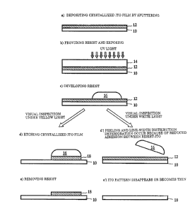
therefore it. is often used. A process for forming the transparent electrode
is shown in Fig. 1. First, a polycrystalline ITO film 12 is formed on a
substrate 10 by a conventional method such as a shuttering method (Fig.
1(a)). A transparent electrode is typically formed to have a thickness of
approximately 400 to 1500 A. A negative chemically amplified resist 14 is
provided directly on the polycrystalline ITO film 12 to have a thickness of
approximately 1.5 to 2.0 ~. m, and a part to be a pixel is irradiated (Fig.
1(b)). Then, the resist 14 is baked optionally and developed to obtain a
resist pattern 1G (Fig. 1(c)). By using this pattern 16 as a mask, the 1TO
film 12 is etched in a etchant, for example, mixed aqueous solution of nitric
acid and hydrochloric acid, and then the ITO film 12 can be patterned.
For the substrate after the resist development, some hinds of visual
inspections, e.g. inspection of pattern defecl=s, inspection of defects,
inspection of contaminants or dust and so on, are performed. These
CA 02351568 2001-05-15
JA998129
inspections are essential to improvements of process yield and stability.
However, it was found that if the substrate is placed under a white light or
a green light for the inspection, adhesion of the resist pattern to the ITO
film is reduced (Fig. 1(d')), and in the ITO etching step which is
subsequently performed, resist peeling or deterioration of line width
distribution occurs (Fig. 1(e')). This problem may be attributed to the fact
that photolysis reaction occurs in the photo-acid generating material
contained in the resist, additional acid is generated in the resist pattern
16, and this acid corrodes the ITO film in i;he boundary between the ITO
film 12 and the resist 16. In order to prevent the generation of additional
acid, all the inspections mentioned above must be carried out under a
yellow light which does not include an absorption spectrum of the
photo-acid generating material, i.e. a light which wavelength of
approximately 380nm or lower should not be included (Fig. 1(d)). Under
the yellow light, no resist, peeling or no deterioration of the line width
distribution occurs (Fig. 1(e)). In practice, however, it is very difficult to
perform satisfactory inspection under the yellow light. Further, not. only
the inspection but. also any steps including carrying before etching of the
ITO film must be carried out under the yellow light while avoiding a white
light. In order to do so, yellow lamps must, be installed not only in an
etching room hut also all kinds of passages, AGV, stochers, and so on.
In order to solve the problem in which acid generated by exposing
the chemically amplified resist diffuses into the electrically conductive
substrate during t;he patterning by using the chemically amplified resist,
Japanese Patens; Laid-Open No. H6(1994)-132208 teaches us t,o provide an
insulating thin film beforehand on the electrically conductive substrate,
and provide t;he chemically amplified resist, thereon. However, the
provision of another layer between the layer t,o be patterned and the resist
leads to increase in t;he number of steps and costs, as well as to reduce in
S~iel d .
CA 02351568 2001-05-15
JA998129
Disclosure of Invention
Ail object of the present invention is to provide a process which
solves a problem involved in resist peeling or reduced adhesion caused by
light exposure after pattern formation, thereby achieving micro-patterning
for an ITO film with a precision and accuracy.
Another object of the present invention is to provide a process for
~rianufacturing a high image quality flat panel display with high yield by
integrating, at a high density, a transparent electrode made of an ITO film.
For this purpose, visual inspection of the patterned transparent electrode
under a white light or a green light should be necessary.
According to the present invention, a novel process for patterning an
ITO film is provided. The process comprises the steps of: preparing an
amorphous ITO film on a substrate; applying a negative chemically
amplified photosensitive material (or resist) directly on the amorphous ITO
film, and exposing and developing the negative chemically amplified
photosensitive material to form a pattern; and removing a part of the
amorphous ITO film which is not covered with the pattern. According to
the process of the present invention, even if the pattern of the chemically
amplified photosensitive material is exposed to a white light or a green
light for visual inspection, no resist peeling or no reduction in adhesion
occurs.
Another advantage of the present invention is that in the step of
removing the part of the amorphous ITO film, relatively mild acid such as
oxalic acid or phosphoric acid can be used as etching solution instead of
using such strong acid as hydrochloric acid or nitric acid. In this way, the
possibility of damage by strong acid during etching, for example, corrosion
of an underlayer made of metal such as aluminum, can be eliminated.
Accordingly, a patterned ITO film can be easily formed even on a metal
feature.
The patterned amorphous ITO film obtained by t=he process of the
CA 02351568 2001-05-15
JA998129
present invention is heated so as to be converted into a microcrystalline
material, thereby obtaining a crystallized ITO film which exhibits chemical
resistance and good electrical conductivity.
According to an aspect of the present invention, a novel process for
manufacturing a TFT substrate used for a flat panel display is provided. A
pixel electrode of this TFT substrate is formed by using the process for
patterning a transparent electrically conductive film, which is provided by
the present invention. Specifically, the process comprises the steps of~
preparing an amorphous ITO film on a substrate providing a negative
chemically amplified photosensitive material directly on the amorphous
ITO film, and exposing and developing the negative chemically amplified
photosensitive material to form a pattern; removing a hart of the
amorphous ITO film which is not covered with the pataern; removing t;he
pattern; and heating the amorphous ITO film to be microcrystallized. V~Tith
the process of the present invention, since visual inspection under a white
light or a green light can be surely performed after the chemically amplified
photosensitive material (resist) is developed to form a resist pattern, a TFT
substrate used for a high image quality flat panel display can be
manufactured with high yield.
Brief' Description of Drawings
Fig. 1 shows a schematic view shoveling a conventional process for
patterning a transparent electrically conductive film.
Fig. 2 shows a schematic view shop-ring a process for patterning a
transparent electrically conductive film according to the present invention.
Best mode for Carrying Out the Invention
The present; 111Ve11t10I1 provides a novel process for micro-patterning
an Indium-Tin-Oxide (I'I'O) film by using a chemically amplified resist.
According to the process of the present invention, first, an amorphous ITO
CA 02351568 2001-05-15
JA998129
film is formed, and patterned by using a chemically amplified resist. Then,
as occasion arises, the patterned amorphous ITO film is converted into a
microcrystalline material by heating to form a usual crystallized ITO film
pattern which exhibits a good electrical conductivity and chemical
resistance.
Fig. 2 shows a process of forming a transparent electrode, i.e., a
patterned transparent electrically conductive film. In Fig. 2(a), an
amorphous ITO film 22 is deposited onto a substrate 20. The amorphous
ITO film 22 is formed by a sputtering method at a substrate temperature
which is usually held at approximately 200°C or lower, preferably at a
relatively low temperature of nearly a room temperature. For example, as
described in Japanese Patent No. 21361)92; sputtering may be performed by
using an In-Sn alloy target and with Ar gas containing 02 gas and H 2O gas
used as sputtering gas.
In Fig. 2(b), a chemically amplified photosensitive material (resist)
24 is directly applied on the amorphous ITO film 22. Preferably, a negative
type chemically amplified photosensitive material 24 should be applied. As
is recited in Technical Paper (Regional Technical Conf., Oct. 30 to Nov. 2,
1988, p.49) written by W. E. Feely and et al, as for such resin, an improved
negative chemically amplified resist which contains a phenol.ic novolak
resin, methylol melamine and photo-acid generator. For this resist, acid
generated by a light is used as a catalyst, and t=he methylol melamine
causes the phenol resin to be cross-linlced so as to be converted to be
insoluble. As a photo-acid generator, opium salt such as diazonium,
iodonimn, sulfonium or the hl:e, ortho-diazo naphthoquinone sulfonium
acid ester, or triazines generators may be used. Pari;icularly, the txiazines
generator is suitably used because of high sensitivity. Acid generated upon
exposure t=o a light. is considered to be erotic acid.
In Fig. 2(c), the film of the chemically amplified photosensitive
material 24 is exposed to energy rays such as uli;raviolet rays, deep
CA 02351568 2001-05-15
JA998129
ultraviolet rays, electron rays or ~ rays in accordance with the pattern. In
the pattern of several microns, use of the ultraviolet ray is convenient. As
usually carried out, by post exposure baling (PEB) and developing the
resist after the exposure, the resist is patterned. A fine line/space pattern
of approximately 2 ~. m is formed.
By the steps hitherto performed, a structure having a resist pattern
2'6, preferably a negative resist pattern 2G, provided on the amorphous ITO
film 22 is formed. This structure obtained in accordance with the present
invention is different from a conventional structure having a resist pattern
provided on a polycrystalline ITO film in that even if exposed under white
light or green light containing a spectrum with a wavelength of
approximately 380nm or lower, no resist. peeling or no reduction in
adhesion occurs. The reason for this is still under investigation, but it, may
be attributed to the fact that even if additional acid is generated in the
resist pattern 26 by white light or the like, the acid can be diffused and
dispersed into the amorphous ITO film 22, and thus no high concentration
of acid for corroding the amorphous ITO film 22 exists in the boundary
between the amorphous ITO film 22 and the resi st film 2G. Accordingly,
the structure obtained in accordance with the present invention enables
visual inspection to be performed under white light or green light without
adversely affecting subsequent steps.
In Fig. 2(d); the substrate which has been subjected to sufficient
visual inspection after the resist, development, determined to be a good
product and provided with the resist pats=ern 26 is patterned by etching the
amorphous ITO film 22 through the pattern 2G used as a masl.. A part of
the amorphous ITO film 22 which is not covered with the resist pattern 2G
is contacted with etching solution to be dissolved and removed. As etching
solution, organic acid such as oxalic acid, as well as relatively mild mineral
acid such as phosphoric acid or sulfuric acid, may be used. Aft-er the
patterning of the amorphous ITO film 22, the resist pal=tern 2G is removed
CA 02351568 2001-05-15
g JA998129
by an appropriate me~hod as usual (Fig. 2(e)).
As chemical resistance, especially acid resistance, of the amorphous
ITO film 22 is low compared with a usual microcrystalline ITO film, the
amorphous ITO film 22 can be dissolved even in such a relatively mild acid
as described above. On the other hand, however, if the amorphous ITO film
22 is incorporated in a product such as a flat panel display or the like,
damage may occur in subsequent steps or during use. Moreover, since the
amorphous ITO film usually shows high resistivity of approximately 5 X
103 ~ ~ cm, a film having lower resistivity must be provided to be used as a
transparent electrode. Thus, in Fig 2(f~, a patterned amorphous ITO film
28 is heated up to reach a temperature of approximately 200°C or
higher,
which is a crystallization temperature of ITO. Preferably, the film is
heated at a temperature of approximately 250°C for about one to t;wo
hours.
13y this heat treatment, the amorphous ITO film 28 is converted into a
microcrystalline material, thereby obtaining a crystallized ITO film 30
which exhibits chemical resistance and low resistivity.
This process for forming the transparent electrode, i.e., the
patterning method of the transparent. electrically conductive film including
the ITO film, is very useful for forming a pixel electrode of a TFT substrate
for a flat panel display, and it can also be applied to a process for
manufacturing a solar battery, electronic parts, a measuring instrument, a
communication device or the like, which needs a transparent electrically
conductive film. If the process is applied to a process for forming a
structure where a transparent electrically conductive film is used as a
heating unit, a microheat,er capable of adjusting a temperature of only a
very limited area can be provided. As a transparent electrically conductive
film. other than i;he ITO film, a transparent. electrically conductive film
which contains an oxide such as an indium oxide film, a tin oxide film (nesa
l~lm), a cadomium-tin-oxide (CTO) or the like is available.
CA 02351568 2001-05-15
JA998129
Embodiment 1
An ITO film (400A) was deposited on a glass substrate held at
approximately 25°C by a sputtering method. This ITO film was an
amorphous ITO film, because it was not heated to a crystallization
temperature or higher. On the other hand, for the purpose of comparison,
an ITO film (400 was prepared on a glass substrate of approximately
150°C by sputtering, and heated at approximately 230° for about
two hours
to form a completely crystallized ITO film.
On both of the amorphous ITO film and the crystallized ITO film.
similar negative chemically amplified resists were provided so as to be
approximately 1.5 ~. m in thickness. The used negative chemically
amplified resists were Fuji Orin FEN 300 N, Clariant (prototype) and
Tokyo Oka TFN-010. Then, the coated resists were exposed t.o ultraviolc;t
radiation of a wavelength of 405nm, subjected t.o PEB at approximately
110°C, and then developed by using usual all~aline aqueous developing
solution to obtain various resist; patterns having line/space widths of
approximately 2 to 100nm. In any combination samples of the substrates
and the resists, no resist peeling or no line defects were identified. Also,
in
any of the samples not exposed to light after development, no resist= peeling
v~~as identified after water rinsing (shower).
The samples were exposed to the light of a fluorescent lamp for about
thirty minutes. Then, the samples were similarly rinsed by water, and for
the resist patterns on the amorphous ITO film, no peeling was identified at
all in the samples using any of the resists. However, undesired peeling of
the resist pattern occurred on the crystallized ITO film. The results are
shown in Table 1. Even in the case of Tokyo Ol:a resist where the
occur~:ence of defect of peeling was smallest, ii: was identified in 34 points
of peeling among G7 patterns.
The patterned amorphous ITO film was heated at a~~proximately
230° for about two hours, thereby converting t;he amorphous lT0 film
into a
CA 02351568 2001-05-15
JA998129
microcrystallized ITO, and then the electrically conductive film of the
crystallized ITO exhibiting resistivity of approximately 1 X 10⁴ ~ -cm was
obtained.
Table 1
Resist/Substrate Amorphous ITO Crystallized ITO
Fuji Orin FEN 300 No peeling 40164 place peeling
N __ _.___-. -
Clariant Prototype No peeling I 60/64 place peeling
-
34/67 lace eelin
Tokyo Oka TFN-01.0 No peeling i - - p p -g_- _-
_.
Embodiment 2
As in the case of Embodiment l, a sample which has each resist
applied onto an amorphous ITO film, subjected to exposure and PEB, and
then developed to form a resist pattern. The resultant sample was exposed
to green light used for actual visual inspection for about thirty minutes.
Then, the sample was rinsed by water (shower) as same as in the case of
Embodiment 1. No resist peeling was identified.
Embodiment 3
As in the case of Embodiment l, a sample which has each resist
applied onto an amorphous ITO film, subjected t;o exposure and PEB, and
i:hen developed to form a resist pats=ern. The resultant sample was left in a
usual indoor environment for half a day. Then, the sample was rinsed by
v~~ater (shower) as same as in t;he case of Embodiment; 1. No resist; peeling
was identified.