Note : Les descriptions sont présentées dans la langue officielle dans laquelle elles ont été soumises.
CA 02377081 2002-03-15
1
TITLE OF THE INVENTION
METHOD OF PRODUCING AN ETCH-RESISTANT POLYMER
STRUCTURE USING ELECTRON BEAM LITHOGRAPHY
FIELD OF THE INVENTION
The present invention relates to a method of producing an etch-
resistant polymer structure on a substrate using electron beam
lithography.
More specifically, the present invention is concerned with the use of an
electron beam to locally polymerize a layer of sterol deposited on a
substrate to produce the etch-resistant polymer structure.
BACKGROUND OF THE INVENTION
The fabrication of ultra-small scale semiconductor devices requires
very high-resolution lithography techniques. The most frequent high-
resolution lithography technique involved in such fabrication is the so-
called polymeric resist-based lithography. PMMA (Poly(Methyl
Methacrylate)) is a polymer that is currently used in the fabrication of
such devices using electron beam lithography ["Materials and
processes for nanomefer lithography'; S. Mackie, S.P. 8eaumont, Solid
State Technology, vol. 28, August 7985, pp. 917 X22]. This polymer is
known mainly for its positive tone resist behavior, which allows the
selective dissolution of the regions exposed to the electron beam while
leaving intact the unexposed regions. Features with resolutions as
small as 10 nm have been demonstrated with PMMA ["10 nm linewidth
electron beam lithography on GaAs'; H. G. Craighead, R. E. Howard,
L.D. Jackel, P.M. Mankiewich, Applied Physics Letters, vol. 42,
January 1983, pp. 38-40] and other comparable resists. However,
CA 02377081 2002-03-15
2
fabrication of some semiconductor devices requires negative tone
resists, in which the regions unexposed to the electron beam are
dissolved while the exposed regions are left intact. Since the area to be
exposed by the electron beam is smaller in the case of low-density
patterns, negative tone resists reduce the exposure time, a major issue
in large-scale device fabrication such as monolithic integrated circuits
or in the case of clear field photomask fabrication using electron beam
lithography.
Negative resists are common in microelectronics applications, as
described in the following patents and articles:
"High sensitivity negative electron resist'; US patent No. 3, 770, 433
(Bartlett et al.) issued on November 6, 1973;
"Plasma developable electron resist process'; US patent No. 4,386, 752
granted to Juey H. Lai on May 31, 1983;
"High resolution electron beam lithography using ZEP-520 and KRS
resists at low voltage'; D.M. Tanenbaum; C.IlV. Lo, M. lsaacson, H.G.
Craighead, M.J. Rooks, K. Y. Lee, W. S. Huang, T.H.P. Chang, Journal
of Vacuum Science and Technology B, vol. 14, Nov.lDec. 1996, pp.
3829-3833; and
"Ultrahigh resolution of calixarene negative resist in electron beam
lithography'; J. Fujita, Y. Ohnishi, Y. Ochiai, S. Matsui, Applied Physics
Letters, vol. 68, February 9996, pp. 9297-1299.
In several negative resists, the electron beam is used to break bonds of
the polymeric chains. This leaves free radicals to create cross-linking
CA 02377081 2002-03-15
3
between the chains, and generates a non-soluble organic compound in
the area exposed to the electron beam ["Epoxy-polymer electron beam
resists'; US patent No. 3,976,035 (Brewer) issued on October 28,
9975]. The resolution of both positive and negative tone resists is
limited since the polymeric nature of the electron sensitive layer and
the molecular dynamic behavior of the development process remove
complete polymer chains. The polymer chains are entangled in a
random manner, and the dimensions of the entanglement structure of
the polymer as well as the diameter of the broken and disentangled
polymeric chains are usually of the order of 5 nm (["Electron resist'; US
patent No. 4,269,962 granted to J. Kalal, B. Bednar, J. Zachoval, J.
Petr, Z. Pelcbauer and F. Svec on May 26, 9989] and ["Nanostructure
technology'; T.H.P. Chang, D.P. Kern, E. Kratschmer, K. Y. Lee, H.E.
Luhn, M.A. McCord, S.A. Rishton, Y. Vladimirsky, IBM Journal of
Research and Development, vol. 32, July 7988, pp. 462-492]). This
impairs the achievement of structures with better resolution and smaller
line edge roughness.
Another drawback of both the positive and negative tone resists
... currently available is the incompatibility of such resists with biological
tissues. Of course, devices to be implanted in the human body such as
cochlear implants, ocular implants and pain-suppressing implants are
designed to come into direct contact with human organs. To obtain
biocompatible devices, the electron-sensitive layers used for the
patterning of the device elements must also be biocompatible.
Otherwise, a thick encapsulating layer of biocompatible material has to
be deposited on the devices to form a barrier for non-biocompatible
material ["Macroparticle distribution and chemical composition of laser
deposited apatite coatings'; V. N. Bagratash~ili, E. N. Antonov, E. N.
Sobol, V. K. Popov, S. M. Howdle, Applied Physic Letters, vol. 66, May
CA 02377081 2002-03-15
4
?985, pp. 245?-2453]. The presence of such an encapsulating layer
obviously constitutes a limitation to the fabrication of some devices.
Finally, the most important drawback is the need for spin-coating such
resists. Spin coating requires mostly flat surfaces with low relief. Abrupt
and/or high structures on the surface of the substrate produces an
uneven spun resist. This causes reduction in the achievable resolution.
Recently, a method has been developed for fabricating an etch
resistant metallsemiconductor compound using direct-write electron
beam exposure (["Fabrication of sub-micron silicide structures on
silicon using resistless electron beam lithography'; US patent iVo.
5,9?8, 743 granted to J: Beauvais, D. Drouin and E. Lavallee on June
29, ? 999] and [ "Method for fabricating submicron silicide structures on
silicon using a resistless electron beam lithography process'; D.
Drouin, J. 8eauvais, R. Lemire, and E: Lavallee, R. Gauvin, M. Caron,
Applied Physics Letters, vol. 70, June ?997, pp. 3020-3023]. According
to this method, the electron-sensitive layer can be evaporated on top of
the substrate prior to electron beam exposure. Similar results have
been attained using electron sensitive inorganic layers ["Fabrication of
metallic structures in the 10 nm region using an inorganic electron
beam resist'; W. Langheinrich, H. 8eneking, Japanese Journal of
Applied Physics, vol. 32, December 7993, pp. 6298-6223]. However,
the sensitivity of such resists remains low, therefore restraining the use
of this process to applications requiring low throughput such as mask
fabrication.
SUMMARY OF THE INVENTION
In accordance with the present invention, there is provided a method of
producing a structure of etch-resistant polymer on a substrate,
CA 02377081 2002-03-15
comprising:
(a) depositing on a face of the substrate a layer of sterol capable of
polymerizing to form the structure of etch-resistant polymer;
(b) exposing a first region of the layer of sterol to an electron beam to
5 locally polymerize the layer of sterol and form the structure of etch-
resistant polymer; and
(c) removing a second region of the layer of sterol which has not been
exposed to the electron beam to leave on the face of the substrate
only the structure of etch-resistant polymer.
The present invention also relates to a method of producing on a
substrate a mask for lithography, comprising:
(a) depositing on a face of the substrate a radiation-absorbing layer;
(b) depositing on the radiation-absorbing layer a layer of sterol capable
of polymerizing;
(c) exposing a first region of the layer of sterol to an electron beam to
locally polymerize the layer of sterol and form a structure of etch-
resistant polymer;
(d) removing a second region of the layer of sterol which has not been
exposed to the electron beam to leave on the radiation-absorbing
layer only the structure of etch-resistant polymer; and
(e) etching from the face of the substrate a region of the radiation-
absorbing layer not covered by the structure of etch-resistant
polymer.
The invention still further relates to a method of producing on a
substrate a mask for X-ray lithography, comprising:
(a) depositing on a face of the substrate a first layer of etch-resistant
material forming a first barrier to a particular etching process;
(b) depositing on the first layer a second layer of X-ray absorbing
CA 02377081 2002-03-15
6
material;
(c) depositing on the second layer a third layer of etch-resistant
material forming a second barrier to the particular etching process;
(d) depositing on the third layer a layer of sterol capable of
polymerizing;
(e) exposing a first region of the layer of sterol to an electron beam to
locally polymerize the layer of sterol and form a structure of etch-
resistant polymer;
(f) removing a second region of the layer of sterol which has not been
exposed to the electron beam to leave on the third layer only the
structure of etch-resistant polymer;
(g) etching a region of the third layer not covered by the structure of
etch-resistant polymer; and
(h) removing, by means of said particular etching process, a region of
the second layer not covered by the structure of etch resistant
polymer.
The foregoing and other objects, advantages and features of the
present invention will become more apparent upon reading of the
following non restrictive description of illustrative embodiments thereof,
given by way of example only with reference to the accompanying
drawings.
BRIEF DESCRIPTION OF THE DRAWINGS
In the appended drawings, in which like reference numerals
correspond to like elements throughout the figures:
Figure 1 is a cross sectional view of a substrate on which a layer (or
film) of sterol has been deposited;
CA 02377081 2002-03-15
7
Figure 2 is a cross sectional view of the substrate and layer of sterol of
Figure 1, showing the formation of a polymer structure within the layer
of sterol by means of an electron beam;
Figure 3 is a cross sectional view of the substrate and layer of sterol of
Figure 1, showing a polymer structure that has been formed on the
substrate;
Figure 4 is a cross sectional view of the substrate and layer of sterol of
Figure 1, in which the unexposed region of the layer of sterol has been
dissolved by, for example, a wet solution to leave only the polymer
structure on the substrate;
Figure 5 is a micrograph showing polymer structures formed from a
layer of cholesterol on a top face of a substrate of nickel, after
dissolution of the unexposed region of the cholesterol layer; and
Figure 6 is a micrograph showing elements of a X-ray mask prototype
fabricated using a layer of cholesterol to pattern a layer of nickel, then
the layer of nickel to pattern a tantalum absorber, this micrograph being
taken at an angle of 70° with respect to the normal.
DESCRIPTION OF THE ILLUSTRATIVE EMBODIMENT
With reference to the appended drawings an illustrative embodiment of
the present invention will now be described.
Figures 1, 2, 3 and 4 illustrate various steps of a method of producing
an etch-resistant polymer structure on a substrate using electron beam
lithography.
CA 02377081 2002-03-15
8
Referring to Figure 1, a layer (or film) of sterol 10 capable of
polymerizing to form a structure of etch-resistant polymer is deposited
on a previously cleaned face 12 of a substrate 14.
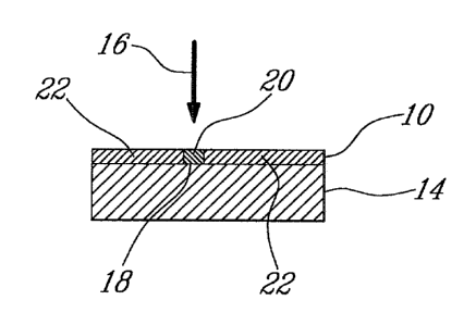
Turning to Figure 2, an electron beam 16 is generated and applied to a
predetermined region 18 of the layer of sterol 10 to locally break
chemical bonds in the sterol molecules, leaving free radicals to form
bonds between the molecules, thus forming an etch-resistant polymer
20. The electron beam 16 can be a focused or shaped electron beam.
With reference to Figure 3, the region 18 exposed to the electron beam
16 (exposed region 18) has been transformed into a structure of etch
resistant polymer 20 due to the above-mentioned polymerization of the
sterol molecules with each other.
With respect to Figure 4, the regions) of the layer of sterol 10 that was
not exposed to the electron beam 16, hereinafter referred to as the
unexposed regions) 22 (see Figures 2 and 3) are removed.
According to another illustrative embodiment, exposure to the electron
beam 16 and removal of the unexposed region 22 of the layer of sterol
10 can be followed by etching of the face 12 of the substrate 14 using
plasma or a wet solution except in the region protected by the structure
24 of etch-resistant polymer 24 (see Figure 4). When etching of the
face 12 has been completed, the polymerized sterol structure 24 can
be removed using oxygen plasma.
CA 02377081 2002-03-15
9
With respect to the above-described illustrative embodiments, what
follows is a brief description of some non-limitative, exemplary features
given for the purpose of illustration only.
The sterol of the layer 10 can be selected from the group consisting of:
agnosterol, avenasterol, brassicasterol, campesterol, cholesterol,
ergosterol, lanosterol, fathosterol, lumisterol, sitosterol, stigmastanol,
and combinations thereof.
The substrate 14 may be made of silicon, metal, etc.
The layer of sterol 10 may be deposited onto the face 12 of the
substrate 14 by a deposition method such as evaporation, Langmuir-
Blodgett deposition, spin coating, dip coating, or any other suitable
technique.
The electron beam 16 may be focused through a series of
electromagnetic lenses or electrostatic Tenses in order to achieve a
minimal beam size on the surface of the sample. Alternatively, it may
be shaped by projection through a stencil to project a corresponding
shape on the surface of the sample. The use of a focused or shaped
electron beam 16 enables the production of a structure 24 of etch-
resistant polymer 20 of sub-micrometer scale resolution, particularly
having linewidths smaller than 100 nm and specifically as small as 50
nm. The etch-resistant polymer structure 24 may be formed, for
example, of ultra-narrow lines of etch-resistant polymer onto the face
12 of the substrate 14. The electron beam 16 may also be displaced,
for example, under the control of a computer to expose a desired
pattern or patterns and to imprint this(ese) patterns) into the layer of
sterol 10.
CA 02377081 2002-03-15
Removal of the unexposed regions) 22 may be accomplished by
dissolving this(ese) regions) through a wet solvent solution. For
example, the sample of Figure 3 can be immersed into a solvent
5 solution capable of dissolving the layer of sterol 10 but incapable of
dissolving the structure 24 of etch-resistant polymer 20. The wet
solution may be selected from the group consisting of: ethers, alcohols,
acetone, methyl ethyl ketone, methyl isobutyl ketone, benzene,
chlorobenzene, ethylbenzene, xylene, toluene, trichloroethylene,
10 chloroform, cellosolve, ethyl acetate, butyl acetate, ethylenediamine,
and combinations thereof. After this dissolution, only the region of the
layer of sterol 10 (structure 24) having been exposed to the electron
beam 16 will remain on the face 12 of the substrate 14.
The invention will be further illustrated by the following non-limitative
examples:
Example 1
In this first example, the method in accordance with the present
invention will be applied to the production of masks for X-ray
lithography.
The fabrication of X-ray masks for industrial applications requires the
patterning of 300 nm to 500 nm thick refractory metal films with high X-
ray absorption coefficient. From the industrial standpoint, tantalum,
tantalum silicide, tungsten and tungsten silicide are usually chosen to
form such absorber layer. To satisfy industrial requirements, the
. patterns are usually required to present a resolution better than 100
nm. In order to achieve this resolution, electron beam lithography is
CA 02377081 2002-03-15
11
used to define the pattern onto an electron sensitive resist applied on
top of the absorber layer.
The pattern is then transferred to an intermediary layer in between the
patterned resist layer on top and the X-ray absorber layer underneath.
This intermediary layer is usually made of SiON, Si02, or of a metal
with an etch chemistry different from the etch chemistry of the absorber
layer; such metal may include, for example, nickel or chromium. The
pattern is transferred from the resist to the intermediary layer by using
plasma or a wet etching solution that will remove this layer, except in
the region protected by the resist pattern.
The pattern is finally transferred from the intermediary layer to the
absorber layer by a reactive ion etching plasma, which removes the
absorber layer in the region left unprotected by the etch of the
intermediary layer.
As a specific example, a 2-~,m thick silicon nitride membrane is
covered with a 50-nm chromium film, followed by a 300-nm tantalum
film, both deposited by argon sputtering. The tantalum film is then
covered by a 20-nm nickel film deposited by thermal evaporation.
In order to perform dip coating, a solution of 1 % of cholesterol in
isopropyl alcohol is prepared. The mask blank is then dipped into the
solution and pulled out of the solution at a regular slow speed, leaving
a 60-nm thick layer of cholesterol on the dried surface. Electron beam
lithography is performed on this cholesterol film using a highly focused
electron beam, at 3 keV. Exposure doses above 500NCIcm2 are used,
creating a sufficient amount of broken chemical bonds in the
cholesterol molecules which leaves free radicals cross linking the
CA 02377081 2002-03-15
12
molecules, forming an etch-resistant polymer in the exposed region(s).
These structures of polymer cannot be dissolved in common solvents
and resist most acid solutions. Lithography is carried out using a JEOL-
6300 Scanning Electron Microscope equipped with a beam blanker.
The position of the beam during the patterning process in externally
controlled by the Nanometer Pattern Generation System by J.C. Nabity
Lithography systems, that writes the different elements of the desired
pattern by displacing the beam on the layer of cholesterol. The pattern
corresponds to the pattern to be projected by the X-ray mask.
After exposure, the mask is dipped into an isopropyl alcohol solution, in
order to remove the unexposed regions) of the layer of cholesterol.
The exposed region(s), being polymerized, is(are) not soluble in this
solution and therefore remain intact. The mask is dried using nitrogen.
The mask is then dipped into a nitric acid solution in order to remove
the thin film of nickel, except in the regions) protected by the
polymerized cholesterol. The sample is then cleaned and dried.
The mask is then processed in a reactive ion etching system, with a
mixture of SF6 and CH4, with a RF power of 80 Watts. The tantalum
film is etched to the bottom, except in the regions) protected by the
nickel. The etching conditions are such that the tantalum structure
defined by this plasma etching has vertical sidewalls. The mask is
water cooled during the etching process in order to avoid fractures or
deformations of the membrane. The layer of chromium acts as a barrier
to the etching plasma. The chromium layer can then be removed, if
needed, by wet etching using a ceric amonium nitrate and perchloric
acid solution.
CA 02377081 2002-03-15
13
Figure 6 shows elements of an X-ray mask fabricated using this
method.
The interest of sterols as electron beam sensitive resists for the
fabrication of such masks comes from the excellent resistance of the
sterol and sterol polymers to protic solvents, such as the acid solutions
used to transfer the pattern from the resist polymer pattern to the
underlying intermediary layer (nickel). The sterols, as part of the lipids,
are generally not soluble in protic solvents, which prevents the
patterned sterol polymer from being dissolved or damaged during wet
etching of the intermediary layer. Also, in the case of X-ray masks, the
substrate is a membrane of the order of 2-p.m thick. Spin-coating
involves high speed of rotation and induces vibrations susceptible to
cause fractures in the material of membrane and produce mechanical
stresses that will cause errors in the image placement of the pattern.
This is a critical issue related to the use of this technology in the
industry. Contrary to conventional resists that require to be spin-
coated, sterols can be either evaporated or spin coated, eliminating
those problems.
In a similar manner, masks for electron projection lithography and
masks for extreme ultraviolet lithography can be fabricated by
substituting the tantalum layer with another type of layer having
absorption characteristics appropriate for the given technology.
Example 2
In this second example, the method in accordance with the present
invention will be applied to the production of masks for deep ultraviolet
photolithography.
CA 02377081 2002-03-15
14
The fabrication of masks for deep ultraviolet lithography (DUV);
requires high-resolution patterning of a layer of absorber such as
chromium, especially for the optical proximity correction patterns that
are used to improve the resolution of the DUV lithography systems.
For the fabrication of a DUV mask according to this second example, a
80-nm thick chromium absorber layer or film is deposited by
evaporation on top of a quartz plate.
A solution of 1 % of cholesterol dissolved in methyl ethyl ketone is
prepared. This solution is used to spin coat at 5000 rpm the electron
sensitive, resist cholesterol layer on top of the chromium layer using
conventional spin-coating equipment. Contrary to conventional resists,
no baking of the electron sensitive cholesterol layer is required after
this layer has been spun. In order to achieve sub-500 nm resolution,
electron beam lithography is used to define the pattern within the
electron sensitive resist layer on top of the absorber layer. Electron
beam lithography is performed at energies above 2 keV in order to
inject electrons deep enough to transform the entire thickness of the
layer of cholesterol into a structure of etch-resistant polymer. Exposure
doses increase as a function of the energy, so typically, energies from
3 to 5 keV are chosen.
After exposure, the mask is dipped into a methyl ethyl ketone solution,
in order to remove the unexposed regions) of the layer of cholesterol.
The exposed region(s), being polymerized, is(are) not soluble in this
solution and therefore remains) intact.
The sample is then dipped into a chromium etching solution of ceric
CA 02377081 2002-03-15
ammonium nitrate and perchloric acid, dissolved in water. This solution
removes completely the chromium layer, except in the region protected
by the resist pattern. The regions) unexposed to the electron beam
therefore becomes) clear fields in the masks.
5
The mask can finally be cleaned using an oxygen plasma etching
system, which will remove the polymerized cholesterol structure
without damaging the underlying chromium layer.
10 Examale 3
In this third example, the method in accordance with the present
invention will be applied to the production of gates for transistors by
direct electron beam lithography.
For the fabrication of, for example, MOSFET transistor gates using the
present technology, a poly-crystalline silicon (poly-Si) layer is deposited
by LPCVD (Low Pressure Chemical Vapor Deposition) on top of an
oxide layer on a silicon substrate. A pattern in the oxide layer was
previously used to define the transistor channels between the sources
and the drains of the transistors.
A 50-nm thick layer of cholesterol is then evaporated on top of the poly-
Si layer, using conventional Joule effect evaporation under vacuum
with controlled deposition parameters (deposition rate, temperature,
pressure) optimized in order to achieve a surface of cholesterol both
uniform and free of morphology defects. Lithography is performed
using a shaped beam lithography system. In such a system, a large
and unfocused electron beam is projected through a stencil mask that
absorbs the electrons, except in the open areas (holes) of the mask.
CA 02377081 2002-03-15
16
The pattern defined by these holes is then projected onto the layer of
cholesterol. In the regions) where electrons are projected in that
manner, the electrons break bonds in the cholesterol molecules,
leaving free radicals to cross-link the molecules, thus forming a
structure of etch-resistant polymer. The entire pattern can be either
formed by scanning a large electron beam over a complex stencil mask
containing the different elements of the pattern, or by projecting the
beam through a simple mask onto different areas of the wafer.
Once the lithography is completed, the wafer is dipped into an
isopropyl alcohol solution for several minutes in order to remove
completely the unexposed regions) of the layer of cholesterol.
The wafer is then rinsed in water, dried with nitrogen, and dipped into a
solution of HF and HN03, diluted in water. This removes completely the
poly-Si, except in regions) protected by the polymerized cholesterol
structure, thus defining the gates of the transistors.
Finally, the etch-resistant polymer can be removed using oxygen
plasma, also cleaning the wafer from residues from wet etching
solutions.
It is to be understood that the invention is not limited in its application to
the details of construction and parts illustrated in the accompanying
drawings and described hereinabove. The invention is capable of other
embodiments and of being practised in various other ways. It is also to
be understood that the phraseology or terminology used herein is for
the purpose of description and not (imitation. Hence, although the
present invention has been described hereinabove by way of
illustrative embodiments and examples thereof, it can be modified at
CA 02377081 2002-03-15
17
will, within the scope of the appended claims, without departing from
the spirit and nature of the subject invention.