Note : Les descriptions sont présentées dans la langue officielle dans laquelle elles ont été soumises.
CA 02387072 2002-04-10
WO 01/29811 PCT/US00/29209
SINGLE HORIZONTAL SCAN RANGE CRT MONITOR
Background of the Invention
This invention relates to computer monitors and, more particularly, to a
single horizontal scan range cathode ray tube (CRT) monitor for use with
personal
computers having differing output display signal formats.
There is little standardization among personal computer (PC) manufacturers
for the resolution and frequency of the display signals generated by the
display
cards of the PCs. On the other hand, it is generally more expensive and
complicated to make analog monitors which can adapt to a plurality of display
signal frequencies. One such possible arrangement is shown in Fig. 1 . In this
arrangement a PC 10 includes a display card (not shown) having a digital to
analog
(D/A) converter 12 to output analog display signals, at a frequency and
resolution
set by the PC, to a CRT multiple scanning frequency monitor 14. The monitor 14
has to detect the frequency and adjust its scanning frequency to match that of
the
initial display signals. Such a monitor is complex and expensive to build.
Still another possible monitor display arrangement is illustrated in Fig. 2.
Again the PC 10 includes a display card (not shown) having a digital to analog
(D/A) converter 12 to output analog display signals, at a frequency and
resolution
set by the PC, to a single scan frequency liquid crystal display (LCD) monitor
16.
The LCD monitor 16 includes an A/D converter 18 that converts the received
analog signals into digital signals. A scaling engine 20 within the LCD
monitor 16
converts the digital display signals into a frequency and resolution that are
compatible with the LCD monitor 16 and supplies them to a display circuit (not
shown) within the LCD monitor 16. In this arrangement, the A/D converter and
the
LCD panel are expensive.
Yet another possible arrangement is illustrated in Fig. 3. In this arrangement
the PC 10 includes a display card (not shown) having a digital to analog (D/A)
CA 02387072 2002-04-10
WO 01/29811 PCT/US00/29209
converter 12 to output analog display signals, at a frequency and resolution
set by
the PC, to an A/D converter 24 of a single scan CRT monitor 22. The output of
the
A/D converter 24 is supplied to a scaling engine 26 that converts the digital
display
signals into a frequency and resolution that are compatible with the CRT
monitor
22 and supplies them to a D/A converter 28. The analog output display signals
of
the D/A converter 28 are supplied to the monitor 22 for display at a
resolution and
frequency compatible with the monitor. The disadvantages of this arrangement
are
also that it is complex to manufacture and expensive.
Lastly, in the possible arrangement of Fig. 4, a PC 30 having an internal
scaling engine 32 outputs digital display signals at a resolution and
frequency
compatible with a single scan LCD monitor 16. While this arrangement has the
advantage of a lower cost host, the LCD panel is still expensive for general
use,
e.g. in desktop PCs.
What is needed is a single horizontal scan range monitor, preferably a CRT
monitor, that is inexpensive, not complex to make, and allows the monitor to
be
compatible with PCs having display circuits that output display signals at a
variety
of different scanning frequencies and display resolutions.
Summary of the Invention
The above and other objectives are obtained by the present invention of a
single horizontal scan range monitor that accepts display signals in a digital
format
from an external source, such as a personal computer. The initial display
signals
can have one of a plurality of input resolutions and scanning frequencies. A
converter supplied with the initial display signals detects the particular
input
resolution of the initial display signals and converts them to digital output
signals
having a vertical output resolution selected from a plurality of different
output
resolutions matched to the detected input resolution of the initial display
signals
and a horizontal scanning frequency that is the same as the horizontal
scanning
frequency of the monitor.
2
CA 02387072 2002-04-10
WO 01/29811 PCT/US00/29209
Preferably the monitor is a cathode ray tube (CRT) monitor. In some
embodiments, the initial display signals are converted to output signals
having a
single predetermined horizontal resolution, regardless of the horizontal
resolution of
the initial display signals. In one preferred embodiment, the converter is an
integrated circuit chip.
The monitor includes a display data input for receiving the initial display
data. This display data input can be a receiver where the external source
transmits
the initial display data in the digital format. In some preferred embodiment,
the
converter is a circuit that includes a frame memory. The display signal
conversion
is accomplished by controlling the data writing and reading rates to the frame
memory. The converter includes, in addition to the frame memory, a resolution
detector for detecting the resolution of the initial display signals and
outputting a
resolution detection signal and a first multiplexer connected between the
display
data input, the frame memory, and the monitor for switching between writing
the
initial display signals into the frame memory and reading the digital output
signals
out of the frame memory to the monitor. An address counter controller controls
the
addresses at which data are written into the frame memory and read out from
the
frame memory. A vertical sync generator connected to the resolution detector
generates a vertical sync pulse for the monitor at a selected one of a
plurality of
vertical sync frequencies as a function of the detected resolution of the
initial
display signals. A horizontal sync generator generates a horizontal sync pulse
at
the single horizontal scanning frequency of the monitor. A data output clock
generator generates a data output clock signal as a product of the single
horizontal
scanning frequency and a multiplier factor equal to the sum of the horizontal
output resolution and a horizontal blanking interval.
A second multiplexer receives from the display data input a clock and a
vertical sync signal. The second multiplexer is connected to the address
counter,
the data output clock signal generator, and the horizontal sync generator for
selectively supplying to the address counter controller either the combination
of the
3
CA 02387072 2002-04-10
WO 01/29811 PCT/US00/29209
vertical sync signal and the clock from the display data input or the
combination of
the data output clock signal from the data output clock generator and the
horizontal sync pulse from the horizontal sync generator. A sector controller
controls the first multiplexer and the second multiplexer to synchronously and
alternately write the initial display data to the frame memory at initial
resolutions
and scanning frequencies and read the digital output data signals from the
frame
memory to the monitor at resolutions and scanning frequencies that are
compatible
with the monitor.
In embodiments where the converter resides in the monitor, it is preferable
to have the display signals transmitted by the PC to the monitor in digital
form. A
receiver is incorporated as part of the display data input of the monitor and
receives the digital display signals and forwards them to the converter. In
the
preferred embodiments, the receiver is one of a transition-minimized
differential
scaling (TMDS) receiver, a low voltage differential signaling (LVDS) receiver,
a low
voltage differential signaling display interface (LDI) receiver, and a gigabit
video
interface (GVIF) receiver.
In one preferred embodiment wherein the receiver is a TMDS receiver, the
clock from the receiver is a transition minimized differential scaling (TMDS)
clock
signal. The horizontal sync generator includes a phase locked loop (PLL)
circuit for
generating the data output clock. In the preferred embodiment, the horizontal
sync
generator generates horizontal sync pulses at a frequency of 80 kHz. The
vertical
sync generator generates vertical sync pulses at a selected one of the
following
frequencies in correspondence with the resolution detection signal: 79.9 Hz,
95.1
Hz, 124.8 Hz, 98.9 Hz, 88.4 Hz, and 75.1 Hz.
The converters of some of the above-discussed preferred embodiments,
particularly those wherein the converter is a integrated circuit, convert the
resolution of the initial display signals according to the following table:
4
CA 02387072 2002-04-10
WO 01/29811 PCT/US00129209
In ut Converted fH(kHz) fV(Hz) Clock (MHz)
640x480 1400x960 80 79.9 151.68
720x400 1400x800 80 95.1 151.68
800x600 1400x600 80 124.8 151.68
1024x768 1400x768 80 98.9 151.68
1152x864 1400x864 80 88.4 151.68
1280x 1024 1400x 1024 80 75.1 151.68
where "Input" is the resolution in pixels of the initial display signals,
"Converted" is
the resolution in pixels of the display output signals, "fH" is the horizontal
frequency of the display output signals in Kilohertz, "fVHz" is the vertical
sync
frequency of the display output signals, and "Clock" is the data output clock
in
Megahertz (which is computed by multiplying fH x (horizontal resolution) x (a
constant). In these examples the constant is approximately 1.35.
In still other embodiments, the conversion of the resolution of the initial
display signals is according to the following table:
In ut Converted fH(kHz) fV(Hz) Clock (MHz)
640x480 1280x960 80 79.9 138.24
720x400 720x800 80 95.1 78.08
800x600 800x600 80 124.8 87.04
1024x768 1024x768 80 98.9 111.36
1152x864 1152x864 80 88.4 125.44
1280x 1024 1280x 1024 80 75.1 138.24
where the constant for computing the Clock is approximately 1.36.
The invention also encompasses the methods embodied in the processing
steps carried out by the elements of the above described single horizontal
scan
range monitors.
The foregoing and other objectives, features and advantages of the invention
will be more readily understood upon consideration of the following detailed
5
CA 02387072 2002-04-10
WO 01/29811 PCT/LTS00/29209
description of certain preferred embodiments of the invention, taken in
conjunction
with the accompanying drawings.
Brief Description of the Drawings
Fig. 1 is a block diagram of a first possible monitor arrangement that
employs a CRT monitor capable of multiple scanning frequencies.
Fig. 2 is a block diagram of a second possible monitor arrangement that
employs a LCD monitor that incorporates an A/D converter and a scaling engine.
Fig. 3 is a block diagram of a third possible monitor arrangement that
employs a CRT single scan monitor.
Fig. 4 is a block diagram of a fourth possible monitor arrangement that
employs a scaling engine in the PC to supply digital output display signals to
an
LCD monitor.
Fig. 5 is a block diagram of a first embodiment of the invention that employs
a digital interface video board in the PC that outputs digital display signals
to a
CRT single scanning frequency monitor incorporating a digital display signal
receiver, memory, scaling engine, and D/A converter.
Fig. 6 is a more detailed block diagram of the embodiment of Fig. 5.
Fig. 7 is a detailed block diagram of a modification of the embodiment of Fig.
5.
Fig. 8 is a timing diagram for use in explaining the reading and writing
operation for the frame memory of the embodiment of Fig. 7.
Figs. 9A and 9B are tables of conversion frequencies and resolutions
performed by the invention in two different embodiments.
Fig. 10 is a block diagram of a second embodiment of the invention.
Detailed Description of the Preferred Embodiment
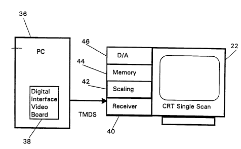
Referring now more particularly to Fig. 5, a first embodiment of the
invention includes a PC 36 having a digital video interface board 38 that acts
as a
6
CA 02387072 2002-04-10
WO 01/29811 PCT/US00/29209
digital display data transmitter. The transmitter can be any one of a
transition
minimized differential scaling (TMDS) transmitter, a low voltage differential
signaling (LVDS) transmitter, a low voltage differential signaling display
interface
(LDI) transmitter, or a gigabit video interface (GVIF) transmitter. The PC 36
outputs
digital display data according to the transmitter's format for resolution, fH
and fV.
In the preferred embodiment, the transmitter is a TMDS transmitter that
transmits
encoded RGB video display data and is manufactured by Genesis Microchip Inc.
The digital data from the PC 36 is supplied to a CRT single scanning
frequency monitor 22 by means of a cable connection or the like. At the CRT
monitor 22, the input display data outputted by the PC 36 is received at a
receiver
40 corresponding to the transmitter 38, that is, the receiver 40 is a
corresponding
TMDS, LVDS, LDI, or GVIF receiver. In this example, it is a TMDS receiver
manufactured by Silicon Image as model no. Sil151. The receiver 40 outputs the
received digital display data to a scaling engine 42 within the CRT monitor
22.
This scaling engine 42 performs a conversion of the digital display signals
output by the PC 36 and received by the receiver 40. This conversion can be
according to the terms of Fig. 9A. For example, for display signals having an
original resolution of 640x480 pixels, the scaling engine 42 outputs digital
display
signals having a resolution of 1400X960 pixels at a horizontal scanning
frequency
(fH) of 80 kHz and a vertical scanning frequency (fV) of 79.9 Hz. The data
output
clock is at the frequency of 151.68 MHz. On the other hand, if the original
resolution of the display signals is 1024x768 pixels, the scaling engine 42
converts
these signals to digital display signals having a resolution of 1400x768
pixels, an
fH of 80 kHz and an fV of 98.9 MHz. In this embodiment, the horizontal
resolution
of the output digital display signals is a constant 1400 pixels irrespective
of the
horizontal resolution of the initial display data.
The scaling engine 42 can be embodied in an integrated chip of the type
described in U.S. Patent No. 5,602,599 and manufactured by Genesis Microchip
Inc., 1999 Concourse Dr., San Jose CA 95131 as models gmZ1, gmZ2, gmZ3,
7
CA 02387072 2002-04-10
WO 01/29811 PCT/US00/29209
gmZd 1, or gmZRX1. Scaling engine 42 can also be a specially programmed
microcomputer.
The scaling engine 42 utilizes either an on-board memory or a memory 44
within the CRT 22 to render the conversion. This memory can be, for example,
dynamic random access memory (DRAM). The digital display signal output from
the scaling engine 42 is converted by a D/A converter (actually separate D/A
converters for each color) and displayed on the single scan CRT 22.
Referring now more particularly to Fig. 6, the embodiment of Fig. 5 is shown
in more detail for the preferred version. In this preferred version the PC 36
has a
digital video interface board 38 that is a TMDS transmitter 48. The digital
RGB
signals in TMDS format are supplied via a cable or other type of connection to
a
TMDS receiver 50 within the CRT monitor 22. One suitable receiver would be
Genesis Microchip Inc.'s model gmZRX1. The TMDS receiver 50 outputs the
initial
display signals as 8 bit digital RGB signals to the scaling chip 44. Within
the
scaling chip 44 is a microprocessor 52 that provides the necessary timing
signals
and calculations for the scaling functions.
The scaling chip 44 writes digital display data to the frame memory 42 that
has separate memory planes for RGB signals. Each memory plane holds, for
example, 1024X768 8-bit color "words", for example, depending upon the
resolution conversion being undertaken. Output digital display data from the
scaling
chip 44 in the form of 8 bit color words for each of the RGB signals are
supplied at
the converted resolution according to the table in Fig. 9A to separate D/A
converters 46R, 46G, and 46B; respectively. The RGB analog output display
signals from the D/A converters 46R, 46G and 46B are supplied to the monitor
22
for display.
Referring now more particularly to Fig. 7, another embodiment of the
invention is illustrated. Elements that are common to the previously described
embodiments have the same reference numbers and their operation will not be
described in further detail. In this embodiment a discrete circuit replaces
the scaling
8
CA 02387072 2002-04-10
WO 01/29811 PCT/US00/29209
chip 44. The eight bit RGB signals output from the TMDS receiver 50 are
supplied
to a first selector switch 54. The selector switch selectively connects each
of the
digital RGB signals either to the input/output (I/O) terminals of a first
dynamic RAM
(DRAM) 58 or to the I/0 terminals of a second DRAM 60. DRAMs 58 and 60
constitute a frame memory. A second selector switch 56 connects the I/O
terminals of the DRAMs 58 and 60 to the D/A converter 46, comprised of the
separate D/A converters 46R, 46G and 46B, which supply analog display signals
to
the monitor 22.
The TMDS receiver also outputs a horizontal sync signal H.SYNC, a vertical
sync signal V.SYNC, and a TMDS clock signal TMDS CLK. The H.SYNC and
V.SYNC signals are supplied to a resolution detector 62. The V.SYNC signal is
also
supplied, along with the TMDS CLK signal, to a third selector switch 68.
V.SYNC
is further supplied to a sector controller 72. The switch 68 alternatively
supplies
V.SYNC to an input of either a first address counter controller 64 or a second
address counter controller 66. The switch 68 simultaneously also alternatively
supplies the TMDS CLK to another input of the first address counter controller
64
or another input of the second address counter controller 66.
The address counter controllers 64 and 66 are connected to the address
lines of the DRAMs 58 and 60, respectively, to control the addresses at which
display data are stored into and read out from the DRAMs 58 and 60. Also
connected to the address counter controllers 64 and 66 is a fourth selector
switch
70. A horizontal sync generator 78 generates 80kHz ("fH") H.SYNC signals which
are supplied to the monitor 22, a phase locked loop (PLL) circuit 74, the D/A
converter 46, a vertical sync generator 80, the sector controller 72, and the
fourth
selector switch 70. The PLL 74 receives the H.SYNC signal having the
horizontal
scanning frequency fH and outputs a data output clock signal (Read CLK) having
a
frequency equal to the product of fH and a multiplier factor from a resolution
multiplier circuit 76. The multiplier factor is equal to the horizontal
resolution of the
display output signals plus a horizontal blanking interval. In the present
example
9
CA 02387072 2002-04-10
WO 01/29811 PCT/US00/29209
Read CLK = fH x (horizontal resolution) x (a constant). Read CLK is supplied
to the
switch 70 and to the D/A converter 46. Note that the vertical sync generator
80 is
supplied with the output of the resolution detector 62. The vertical sync
generator
80 changes the frequency fV of its output V.SYNC signal to the monitor 22 in
correspondence with the detected resolution of the initial display signals, as
is
shown in Fig. 9B.
The sector controller 72 controls the operations of the switches 54, 56, 68
and 70. In operation, the switches 54 and 56 operate synchronously as a first
multiplexer so that while selector switch 54 is connected to supply input
display
signals to be written into DRAM 58, switch 56 is connected to read out stored
display signals from DRAM 60 to the monitor 22 through the D/A converter 46.
The switches 68 and 70 constitute a second multiplexer and the sector
controller
72 controls the switches 68 and 70 to operate synchronously with each other
and
tt~e switches 54 and 56 so that while the switch 54 is connected to write
display
data to DRAM 58 and switch 56 is connected to read display data out of DRAM
60, switch 68 is connected to supply the TMDS CLK signal and the V.SYNC signal
from the TMDS receiver 50 to address counter controller 64. Simultaneously,
the
sector controller 72 also causes the switch 70 to supply the Read CLK signal
from
the PLL 74 and the H.SYNC signal from the horizontal sync generator 78 to the
address counter controller 66.
The sector controller 72 also controls the switches 54, 56, 64 and 66 to
simultaneously change their connections to be connected to the other of the
two
DRAMs 58 and 60 and address counter controllers 64 and 66, respectively. In
this
way, a first set of received digital display data from the receiver 50 are
written into
DRAM 58 at one resolution and set of frequencies while a second set of
received
digital display data are read out of DRAM 60 at a different resolution and set
of
frequencies. Then the process is reversed by causing the switches 54, 56, 68
and
70 to simultaneously change over their connections to the other of the two
DRAMs 58 or 60, respectively, and the first set of display data are read out
of
CA 02387072 2002-04-10
WO 01/29811 PCT/US00/29209
DRAM 58 at the converted resolution and frequencies while a third set of
received
display data from the TMDS receiver 50 are stored in the DRAM 60.
Referring now more particularly to Fig. 8, the timing of the process for
reading and writing to the DRAMs 58 and 60 will be described in more detail.
As
illustrated in the figure, writing of the input display data received from the
Receiver
50 to the frame memory DRAMs 58 and 60 is controlled by the 60 Hz V.SYNC
signal from the Receiver 50. In the figure, this is indicated by the first
"input'
period 82 for DRAM 56. The reading out of data from the DRAMs 58 and 60 to
the monitor 22 is synchronized with the 98.9 Hz V.SYNC signal from the V.SYNC
generator 80. This is illustrated by the output period 84 when the display
data are
read out from the DRAM 60. The display data stored in the DRAM 58 are next
read out at period 86. It is to be understood that the particular fH and fV
values
used here are merely examples.
All the display data stored in one of the DRAMs 58 or 60 can be read out in
two 98.9 Hz V.SYNC periods, however, the writing time to the DRAMs is shorter
in duration. Note that the duration of the output period 84 exceeds the
duration of
the input period 82. Because the data writing and data reading periods are
unequal
in duration, after the first data read/write cycle there is a period during
which there
might be an overlap of reading and writing operations for the same memory. For
example, all of the display data may have been read out from one of the DRAMs
before all of the data have been input to the other DRAM. In this case, the
DRAM
being read out is simply read out again so that the same data are redisplayed.
This
is illustrated in time periods 90 and 92.
After period 86, for example, display data are read out from DRAM 60 for
the first two of three consecutive 98.9 Hz V.SYNC periods during period 90.
Because DRAM 58 is being written to at the timing of V.SYNC from the Receiver
50, the writing of received display data to DRAM 58 is not completed until
more
than two 98.9 Hz V.SYNC periods have elapsed since the beginning of period 90.
That is, all of the display data have been read out from the DRAM 60 before
the
11
CA 02387072 2002-04-10
WO 01/29811 PCT/US00/29209
process of writing data to the DRAM 58 has been completed during period 92.
Thus, DRAM 58 is not ready to be read from at this time. Therefore, the
display
data once read out from DRAM 60 during the first part of period 90 are again
read
out for the last 98.9 Hz V.SYNC interval 94 of period 90. The viewer of the
monitor 22 is not even aware that the same display data are being repeated.
Thereafter, the display data are read out from DRAM 58. This process repeats
during every display data read/write cycle thereafter.
In the above-described embodiment, the scaling engine resides in the
monitor. However, in another embodiment the scaling engine can reside within
the
PC. Referring now more particularly to Fig. 10, a second embodiment of the
invention includes a PC 30 having a scaling engine 34 incorporated therein.
This
scaling engine 34 performs the same conversion of the digital display signals
output within the PC 30 and outputs the converted digital display signals to a
D/A
converter 28 of the single horizontal scanning frequency CRT monitor 22 for
display. This conversion can be according to the terms of Fig. 9A. The
horizontal
scanning frequency of the monitor 22 is fH, which in the preferred embodiments
described herein is 80 kHz. The scaling engine 34 can also be embodied in an
integrated circuit chip of the type described in U.S. Patent No. 5,602,599 and
manufactured by Genesis Microchip Inc., 1999 Concourse Dr., San Jose CA
95131 as models gmZ1, gmZ2, gmZ3, gmZd1, or gmZRX1. Scaling engine 34 can
also be a specially programmed microprocessor. Further, the scaling engine 34
can
have essentially the same construction as the circuit of Fig. 7 with the TMDS
receiver 50 being replaced by the display adapter of the PC 30. In this
embodiment, the conversion is according to Fig. 9B.
Described above is a single horizontal scan range CRT monitor that enables a
single scan CRT to be economically and conveniently interfaced to PCs having
different digital display outputs.
Although the present invention has been shown and described with respect
to preferred embodiments, various changes and modifications are deemed to lie
12
CA 02387072 2002-04-10
WO 01/29811 PCT/LTS00/29209
within the spirit and scope of the invention as claimed. The corresponding
structures, materials, acts, and equivalents of all means or step plus
function
elements in the claims which follow are intended to include any structure,
material,
or acts for performing the functions in combination with other claimed
elements as
specifically claimed.
13