Note : Les descriptions sont présentées dans la langue officielle dans laquelle elles ont été soumises.
WO 01/37313 CA 02391911 2002-05-15 PCT/EP00/09997
TITLE OF THE INVENTION
Plasma processing apparatus with an electrically conductive wall.
s FIELD OF THE INVENTION
The present invention pertains to a plasma processing apparatus useful
in plasma-assisted processes such as etching, deposition or sputtering
processes. More particularly, the invention relates to an Inductive Coupled
io Plasma source.
BACKGROUND OF THE INVENTION
Inductive Coupled Plasma sources are conventionally used for etching
1s substrates or depositing material thereon. They are generally composed of a
plasma chamber having a lateral dielectric wall surrounded by an external
solenoid inductor. The plasma chamber contains a process gas. The external
inductor is fed by a Radio Frequency generator and produces electromagnetic
energy which is provided to the interior of the plasma chamber through the
?o dielectric wall. A plasma is thus generated inside the chamber, by
ionization
of the process gas molecules.
The composition of the process gas is selected as a function of the
treatment to be applied to the substrate. Thus, for example, if the plasma
apparatus is used for material deposition on a substrate, the process gas will
25 contain material elements to be deposited on this substrate. If the plasma
apparatus is used as an etching apparatus, the process gas will contain
reactive species that will react with the substrate and remove material
therefrom.
An interesting characteristic of the plasma-assisted processes, in
30 particular with respect to the Chemical Vapour Deposition technique, is
that,
by virtue of the use of the plasma, a lower substrate temperature is required
in
order to activate the reaction or deposition. Plasma-assisted processes may
therefore be advantageously applied notably when the substrate to be treated
cannot withstand high temperatures.
CA 02391911 2008-06-20
-2-
However, Inductive Coupled Plasma sources remain expensive, in
particular when they are shaped so as to have curved portions. The material
from wlli.ch their extetnal wall is made, i.e. a dielectric material, is
indeed not
appropriate for the manufacture of complex pieces, such as curved or
cylindrical pieces. Furthermore, drilling a hole in the dielectric material,
for
example in order to provide an access to the interior of the chamber for the
process gas, is a difficult task.
WO-A-96/41897 describes a plasma treatment apparatus comprising a
parallelepiped plasma chamber surrounded by electrical conductors. The side
walls of the plasma chamber are composed of parallel metallic bars extending
longitudinally over the length of the chamber. Gaps or slots are defined
between the metallic bars in order to allow the maanetic field produced by
the electrical conductors to penetrate into the interior of the plasma
chamber.
The plasma chamber is sealed by dielectric plates, each covering the external
side of a corresponding chamber side wall.
The use of a dielectric plate for each side wall of the chamber may
pose a problem when it is desired to have a chainbet- with a more coinplex
shape, such as a cylindrical shape. Curved dielectric plates ~vould indeed
have to be constructed, which would significantly increase the manufacturing
costs. Furthermore, the plasma chamber according to WO-A-96/41897 is not
appropriate for providing a lateral access for the process gas. since such
lateral access would require drilling a hole through a dielectric plate,.
SUMMARY OF THE PRESENT INVENTION
The present invention aims at remedying the above-mentioned
drawbacks.
According to the present invention, there is provided a plasma processing
apparatus comprising:
a plasma chamber comprising an electrically conductive wall, wherein
said electrically conductive wall has one or more aperture for interrupting a
current path in said wall when electromagnetic energy is provided into the
chamber from the outside of the chamber,
external electromagnetic means for supplying electromagnetic energy
into said plasma chamber through said electrically conductive wall in order to
CA 02391911 2008-06-20
-3-
create a plasma inside the chamber, and
sealing means for sealing said at least one aperture,
characterised in that said sealing means comprises one or more electrically
conductive closing element, and in that each aperture is sealed with one of
said
closing elements which is mounted on the external surface of said electrically
conductive wall, said electrically conductive closing elements being
electrically
insulated from said electrically conductive wall.
Preferably, according to the present invention, one or more electrically
conductive enclosure elements are used to seal the aperture(s) defined on the
conductive wall of the plasma chamber. The plasma chamber is therefore
essentially made from an electrically conductive material, such as metal,
which
renders the construction of the chamber more flexible. In particular, the
chamber
may have a complex shape, without the manufacturing costs significantly
increasing, since conductive materials may be machined and deformed rather
easily.
Preferably, furthermore, as the conductive enclosure elements are
electrically insulated from the conductive wall, a current path through the
conductive wall is interrupted at the level of the aperture(s), thus
preventing a
current loop to be formed all around the conductive wall when electromagnetic
energy is supplied to the interior of the chamber. By virtue of the provision
of the
aperture(s) and of the fact that the conductive enclosure element(s) is
insulated
from the conductive wall, the electromagnetic energy produced by the external
electromagnetic means is not or little screened out by the conductive wall. An
important portion of the electromagnetic energy produced by the external
electromagnetic means is therefore effectively supplied to the inside of the
chamber.
Preferably, said at least one aperture extends in a first direction which is
substantially parallel to the magnetic field induced by the external
electromagnetic means, so as to interrupt a current path through the
electrically
conductive wall in a direction orthogonal to said first direction.
Preferably, in practice, the electrically conductive wall extends in a
direction parallel to a longitudinal axis of the plasma chamber, and said at
least
one aperture extends in a direction which is substantially parallel to the
longitudinal axis of the plasma chamber, so as to interrupt a current path
CA 02391911 2005-11-08
-4-
through said electrically conductive wall in direction orthogonal to said
longitudinal axis.
The plasma chamber may further comprise end plates at opposite ends
of the electrically conductive wall, which end plates extend perpendicularly
to the conductive wall.
The plasma chamber may be cylindrical, with the electrically
conductive wall forming the cylindrical face of the plasma chamber, or
parallelepiped, with the electrically conductive wall being composed of plane
adjacent faces of the chamber. The plasma chamber may also be of any other
suitable shape, and in particular of a shape that is adapted to the shape of
the
substrate to be plasma treated.
The external electromagnetic means may comprise an inductor
surrounding the electrically conductive wall and connected to an AC power
supply.
Preferably, according to the present invention, at least one insulating
means or electrically non-conductive gasket is provided fro electrically
insulating
each conductive enclosure element from the conductive wall.
Preferably, each non-condiictive gasket is disposed on the conductive
wall in such a manner as to be in indirect line of sight from the interior of
the
chamber, i.e. from the plasma generated inside the chamber. This feature is
particularly advantageous when the plasma processing apparatus according to
the invention is used for depositing or sputtering electrically conductive
material, such as metal. Indeed, in such a case, there would be a risk that a
continuous layer of such conductive material be coated on the non-
conductive gasket when the plasma deposition or sputtering process is being
carried out. This could result in the creation of a current loop all around
the
conductive wall of the chamber and, accordingly, in the electromagnetic
energy supplied by the external electromagnetic means being screened out by
this continuous layer in the manner as explained above.
By avoiding any direct line of sight between the interior of the
chamber and the insulating gasket, the risk of energy screening out due to
conductive material deposition on the chamber wall is prevented or at least
CA 02391911 2005-11-08
-5-
greatly reduced. This result is attained without the present invention
requiring any Faraday shield within the chamber, nor any additiora.al complex
labyrinth structure, as conventionally used in the prior art. Preferably-, as
the enclosure element(s) is/are made of a conductive material, such as metal,
the deposition of conductive material thereon is iiot detrimental. The present
invention makes it thus possible to use wide apertures or slots on the
conductive wall in order to simplify the construction of the apparatus and to
reduce its cost.
Preferably, said at least one aperture consists of a plurality of apertures,
said at least one electrically conductive enclosure element consists of a
plurality
of electrically conductive enclosure elements, and each one of the plurality
of
conductive enclosure elements is mounted on the electrically conductive wall
in
registration with a corresponding one of the plurality of apertures.
Preferably, according to an embodiment of the present invention, said at
least one gasket consists of a plurality of gaskets, each one of the plurality
of
gaskets surrounding, on an external surface of the electrically conductive
wall, a
corresponding one of the plurality of apertures, and each one of the plurality
of
electrically conductive enclosure elements is applied on a corresponding one
of
the plurality of gaskets.
Preferably, according to another embodiment of the present invention,
each one of the plurality of apertures comprises a narrow portion emerging
into
the plasma chamber and a wider portion communicating with the narrow portion
and forming a recess on an external surface of the electrically conductive
wall.
Each one of the plurality of gaskets surrounds, in the recess of a
corresponding
aperture, the narrow portion of the corresponding aperture, and each one of
the
plurality of conductive elements is applied on a corresponding gasket in the
recess of a corresponding aperture.
Preferably , the at least one gasket and the at least one conductive
enclosure element are removably mounted on the conductive wall.
Preferably, a gap between the at least one conductive enclosure element and
the conductive wall is determined according to the Paschen's law, such that
no plasma is generated between the conductive enclosure element(s) and the
conductive wall. Typically, the gap may be less than one millimetre.
CA 02391911 2005-11-08
-6-
The plasma chamber may further comprise one or several sputtering
targets. These sputtering targets may be disposed on an inner surface of the
conductive wall. An insulating plate may be interposed between the
sputtering targets and the inner surface of the conductive wall. The
sputtering source may be connected to a power source by a lead crossing the
conductive wall and electrically.inqqlated from the conductive wall.
According to another preferable feature of the present invention,
the plasma chamber comprises at least one gas inlet formed on the electrically
conductive wall. This gas inlet serves to supply the inside of the chamber
with a process gas. Preferably, the at least one gas inlet consists of a
plurality
of gas inlets provided at regular intervals on the electrically conductive
wall.
The process gas can thus be introduced into the chamber with a uniform
distribution.
In addition to the above-mentioned gas inlets, the plasma chamber
may further comprise one or more gas inlets formed on a cover plate disposed
at the top or the bottom of the chamber. The gas inlets on the conductive
wall may then serve to supply the interior of the chamber with a reactive gas
mixture, while the gas inlets provided on the cover plates may be used for
introducing inert gases whose role notably consists in facilitating the mixing
of the various elements contained in the gas mixture. The gas inlets provided
on the conductive wall, which forms a lateral wall of the chamber, enable the
introduction of the reactive gas mixture into the chaniber in an area close to
the substrate to be treated. In this way, the present invention avoids
supplying the reactive gas mixture to areas which are remote from the
substrate and which therefore need not receive the gas mixture.
In practice, the at least one electrically conductive enclosure element
preferably consists of one or several plates, and both the conductive wall and
the plates are made of metal. Furthermore, the at least one aperture may take
the form of one or several slots.
BRIEF DESCRIPTION OF THE DRAWINGS
Figure 1 is a partial sectional front view of a plasma apparatus
according to a first embodiment of the present invention ;
CA 02391911 2005-11-08
-6a-
Figures 2 and 3 are perspective views respectively showing a plasma
apparatus according to the invention with a cylindrical shape and a
rectangular parallelepiped shape ;
/
CA 02391911 2002-05-15
WO 01/37313 PCT/EP00/09997
-7-
Figure 4 is a diagrammatic front view of a part of a plasma chamber
wall included in the plasma apparatus shown in Figure 1;
Figure 5 is a diagrammatic top view of a part of a plasma chamber
wall included in the plasma apparatus shown in Figure 1;
Figure 6 is a diagrammatic top view of a part of a plasma chamber
wall included in the plasma apparatus shown in Figure 1, illustrating current
paths ;
Figure 7 is a diagrammatic top view of a part of a plasma chamber
wall included in a plasma apparatus according to a second embodiment of the
io present invention ;
Figure 8 is a diagrammatic top view of a part of a plasma chamber
wall included in a plasma apparatus according to a third embodiment of the
present invention ;
Figure 9 is a sectional front view showing a plasma apparatus
according to a fourth embodiment of the present invention ;
Figure 10 is a top sectional view of the plasma apparatus according to
the fourth embodiment of the present invention ;
Figure 11 is a partial sectional front view showing a plasma apparatus
according to a fifth embodiment of the present invention ; and
Figure 12 is a diagrammatic top view of a part of a plasma chamber
wall included in a plasma apparatus according to a sixth embodiment of the
present invention.
DETAILED DESCRIPTION OF THE PRESENT INVENTION
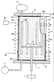
Figure 1 shows an Inductively Coupled Plasma apparatus according to
a first embodiment of the present invention. The plasma apparatus according
to this first embodiment is used as a Plasma Enhanced Chemical Vapour
Deposition apparatus, in order to deposit material layers on substrates.
It generally comprises a plasma, or process, chamber 1 containing a
process gas, an external inductor 2 for creating a plasma inside the plasma
chamber 1, a holder 3, disposed within the plasma chamber, for supporting a
substrate 4, a pump device 5 for evacuating the plasma chamber 1, and a gas
WO 01/37313 CA 02391911 2002-05-15 PCT/EP00/09997
-8-
controller 6 for supplying the plasma chamber with the said process gas
through a gas inlet 6'.
The holder 3 is connected to a power source 7 thereby enabling the
substrate 4 to be biased. The holder 3 may also be connected to a heating or
cooling system (not shown) for temperature regulation of the substrate.
The pump device 5 serves to evacuate the plasma chamber 1 before
the latter is used. The gas controller 6 supplies a process gas composed of a
reactive gas, comprising species that are to be deposited on the upper surface
of the substrate, and an inert gas, enabling an efficient mixing of the
various
io compounds contained in the process gas.
The inductor 2 is connected to a Radio Frequency (RF) power source
20 and provides RF magnetic energy, the frequency of which preferably
ranges between 100 kHz and 100 MHz. Such RF magnetic energy permits
the transformation of the process gas into a plasma, whose reactive species
1s will deposit on the substrate 4.
The general characteristics and operation of a plasma apparatus are
known to the skilled person, and will not therefore be explained in detail.
The plasma chamber 1 according to the present invention may have a
cylindrical shape, as shown in figure 2, or any other suitable shape adapted
to
20 the shape of the substrate 4. Figure 3 shows, as an example, a plasma
chamber according to the invention having a parallelepiped shape.
The plasma chamber 1 comprises a lateral wall 10 extending along and
about a longitudinal axis 11 of the plasma chamber and facing the inductor 2.
The lateral wall 10 is cylindrical in the case of a cylindrical plasma
chamber,
25 or constituted by four plane wall portions if the plasma chamber has a
parallelepiped shape. The plasma chamber 1 further comprises upper and
lower end plates 12, 13 which are perpendicular to the longitudinal axis 11.
The upper and lower end plates 12, 13 are respectively sealed to end surfaces
101, 102 of the lateral wall 10 by vacuum seals 14, 15.
30 According to the present invention, the lateral wall 10 of the plasma
chamber 1 is made of a conductive material, such as metal. Furthermore, a
plurality of apertures 100 are defined through the whole thickness t of the
lateral wall 10 (see figure 5). The apertures 100 preferably extend in a
direction parallel to the longitudinal axis 11, in the form of slots. The
CA 02391911 2002-05-15
WO 01/37313 PCT/EP00/09997
-9-
apertures 100 may extend over the whole length of the plasma chamber, i.e.
between the end surfaces 101, 102 of the lateral wall 10, to contribute to the
formation of a plasma in a large area within the chamber, or over a
substantial portion of this length, as shown in figure 1.
The inductor 2 surrounds the lateral wall 2 at the outside of the plasma
chamber in order to generate, within the chamber 10, an inductive field
whose lines are parallel to the longitudinal axis 11 and to the slots 100.
Figures 4 and 5 show in more detail the apertures 100 formed on the
conductive wall 10, in the case where the plasma chamber 1 is parallelepiped.
to Each aperture 100 is composed of a narrow portion 101 emerging into the
inside of the plasma chamber 1, and a wider portion 1.02 defined on the
external surface 103 of the conductive wall 10 and forming a recess which
communicates with the narrow portion 101. The recess 102 has a larger
width w (orthogonal to the longitudinal axis 11) and preferably a larger
length 1(parallel to the longitudinal axis 11) than those of the narrow
portion
101, as shown in figure 4.
According to the present invention, the apertures, or slots, 100 are
sealed, i.e. hermetically closed, by conductive enclosure elements 16 which
close the apertures and by vacuum seals or gaskets 17 which electrically
insulate the conductive enclosure elements 16 from the conductive wall 10.
The conductive enclosure elements 16 are made of a metal, such as
aluminium. They preferably have the same shape as that of the recesses 102
(rectangular on figure 5), but a slightly smaller size. The conductive
enclosure elements 16 may each take the form of a plate, which may be plane
if the chamber 1 is parallelepiped or curved if the chamber 1 is cylindrical.
The gaskets 17 are made of an insulating material, such as a dielectric
material.
The conductive elements 16 are mounted within the recesses 102 by
appropriate electrically non-conductive mounting members 18. Two
mounting members 18, disposed over opposite lateral sides of the recess 102,
are provided in order to mechanically fit a given conductive element 16 to the
wall 10. Each mounting member 18 has a surface portion 180 which is fixed
on the external surface 103 of the conductive wall 10 and another surface
portion 181 on which a peripheral portion of the upper surface of the
WO 01/37313 CA 02391911 2002-05-15 PCT/EP00/09997
- 10-
conductive element 16 is fixed. Fixing of the mounting members 18 to the
wall 10 and the conductive element 16 may be carried out by bonding or
screwing.
The gaskets 17 preferably have a shape corresponding to that of the
recesses 102 and the conductive elements 16, i.e. rectangular in the
embodiment shown in figures 4 and 5. Each gasket 17 is disposed between a
lower surface of the recess 102 and a peripheral portion of the lower surface
of the conductive element 16, thereby sealing the aperture 100.
The apertures 100 serve to interrupt a current path through the
io conductive wall 10 or, in other words, to break down circulating currents
induced in the conductive wall 10 into plural current loops. Indeed, the
current induced by the RF inductor 2 in the conductive wall 10 would, in the
absence of such apertures, define a continuous loop around the wall 10,
which would screen out the electromagnetic energy delivered by the RF
inductor 2. As illustrated in figure 6, according to the present invention,
currents 19 are induced in each electrically conductive parts, namely the wall
portions on both sides of an aperture 100, and each conductive element 16,
but there is no current path that surrounds the conductive wall 10.
Preferably, the gaskets 17 are each disposed in such a manner as to be
in indirect line of sight froin the interior of the chamber 1. As shown in
figure 5, fhere is thus no direct line of sight 170 between each gasket 17 and
the interior of the chamber 1. This is achieved, for example, by the
conductive enclosure element 16 being much wider than the narrow portion
101 and the gasket 17 being disposed close to the periphery of the conductive
element 16. Such an arrangement makes it possible to avoid the possible
formation of conductive layers on the gasket 17 when the plasma chamber I
is used for depositing conductive material, such as metal, on the substrate 4.
With reference to Figure 7, a plasma apparatus according to a second
embodiment of the present invention differs from the first embodiment as
previously described essentially in that the apertures 100a do not comprise
any recess. Instead of being mounted in a corresponding recess, each
conductive enclosure element 16a is mounted on the external surface 103a of
the conductive wall 10a by non-conductive mounting members 18a and, for
this purpose, has dimensions (length, width) larger than that of the
WO 01/37313 CA 02391911 2002-05-15 PCT/EP00/09997
-11-
corresponding aperture 100a. A gasket 17a surrounding the aperture 100a
seals the gap between the conductive element 16a and the conductive wall
10a.
With reference to Figure 8, a plasma apparatus according to a third
s embodiment of the present invention differs from the first embodiment as
previously described essentially in that :
- seals 20b are provided between the non-conductive mounting
members 18b and the conductive elements 16b, and
- the seal 17b which surrounds the narrow portion 101 b of a given
i o aperture 1 OOb has a flat shape thereby defining an accurate gap d between
the
corresponding conductive element 16b and the conductive wall 10b in a
direction transverse to the longitudinal axis 11 of the plasma chamber 1.
In this third embodiment, the gap d is adjusted according to the
Paschen's law, such that no plasma is created therein. Typically, for an
1s operating pressure inside the plasma chamber of 100 mTorr, the gap d is
less
than 1 mm. The adjustment is carried out by using several calibrated inserts
with different thicknesses for the seal 17b. The seal 17b, the conductive
element 16b, the seals 20b and the mounting members 18b are removably
mounted, thus enabling the replacement, on the plasma chamber, of the insert
20 17b by another insert having a different thickness.
Figures 9 and 10 show a plasma apparatus according to a fourth
embodiment of the present invention. The plasma apparatus according to this
fourth embodiment essentially has the same structure as that of the first
embodiment as previously described, except that one or several gas inlets 6c'
25 are provided on the lateral conductive wall lOc, and one or several gas
inlets
6c" are provided on the upper end plate 12c.
As shown in figure 10, the gas inlets 6c' formed on the lateral wall l Oc
are disposed at regular intervals between each other. The gas inlets 6c' serve
to supply the interior of the plasma chamber 1 c with a gas mixture containing
30 the reactive species. The gas inlets 6c" formed on the upper end plate 12c
serve to supply the interior of the plasma chamber 1 c with an inert gas,
whose
role notably consists in facilitating the mixing of the various elements
contained in the reactive gas mixture. The arrangement as illustrated in
figures 9 and 10 has the advantage of enabling a gas injection in an area
close
WO 01/37313 CA 02391911 2002-05-15 PCT/EP00/09997
- 12-
to the substrate 4c to be treated, thus avoiding to supply process gas to
areas
within the chamber 1 c which need not receive such gas. Furthermore, the
fact that the gas inlets 6c' on the lateral wall lOc are placed at regular
intervals permit to have to uniform distribution of the gas mixture within the
chamber 1 c in the area of the substrate 4c.
Figure 11 shows a plasma apparatus according to a fifth embodiment
of the present invention. The plasma apparatus according to this fifth
embodiment serves to carry out a sputtering process, wherein material to be
deposited on a substrate is sputtered from a target.
The construction of this plasma apparatus differs from that of the first
embodiment in that a target 21 d, i.e. a material source, is sealed on the
upper
plate 12d of the plasma chamber ld. A DC voltage source (or DC pulsed
source) 22d is connected to the target 21 d to enable the sputtering of the
material to be deposited. As the plasma chamber 1 d is preferably grounded,
the target 21d is electrically isolated from the upper plate 12d by an
insulating ring 23d. A magnetron (not shown) may be added to this
arrangement to enhance the sputtering efficiency. In this case, the gas inlet
6d' connected to the gas controller 6d is placed on the top of the lateral
wall
10d.
Figure 12 shows a sixth embodiment of the present invention. The
plasma apparatus according to this sixth embodiment is identical to that of
the first embodiment, except that it comprises sputtering targets 24e disposed
on the conductive wall 10e towards the interior of the plasma chamber. The
sputtering targets 24e are made from the material to be deposited on the
substrate. Preferably, the conductive wall 10e is grounded, and the targets
24e are electrically insulated from the conductive wall 10e by electrical
insulators 25e. Each target 24e is connected to a DC voltage source or a DC
pulsed source 26e by an electrical lead 27e in order to enable sputtering
operations. Each electrical lead 27e is electrically insulated from the
conductive wall 10e by seals 28e.
In each one of the six embodiments described above, cooling means
may be provided in order to cool the conductive wall 10, 10a, IOb, lOc, lOd,
for example in the manner as explained in EP-A-0908922.