Note : Les descriptions sont présentées dans la langue officielle dans laquelle elles ont été soumises.
CA 02414459 2002-12-16
Doc. No. P1606 CA Patent
INTERFERENCE FILTER FOR OPTICAL TELECOMMUNICATION
Related applications:
[O1 ~ This application claims priority from IJS Provisional application No.
60/341,454 filed
December 17, 2001, the disclosure of which is incorporated herein by
reference.
BACKGROUND OF 'THE INVENTION
[02J Mach-Zehnder and Michelson interferometers are commonly known in optical
telecommunication. The first Mach-Zehnder interferometers (MZI) built for
balanced receiver
applications utilized glass ion exchange waveguides with a 3 dB coupler. These
devices were
found to have too much polarization dependence. This made biasing the
interferometer difficult
because the polarization state at the receiver was random and varied with
time. This meant that
the desired bias point of the interferometer needed to vary with the same
dynamics as the input
polarization state which is unknown.
[03 ] It is known, for example from Yonenaga et al., "Dispersion-Tolerant
Optical
Transmission System Using Duobinary Transmitter and Binary Receiver", Journal
of Lightwave
Technology, Vol. 15, No. 8, August 1997. pages 1530-1 X37, and from Yonenaga
et al. U.S. Pat.
No. 5,543,952 issued Aug, 6, 1996 and entitled "Optical Transmission System",
to use duobinary
code for a modulating signal supplied in push-pull manner to a dual-drive Mach-
Zehnder (MZ)
type optical intensity modulator in an optical communications system. The use
of duobinary code
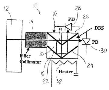
in this manner reduces the signal bandwidth required for a given signal
transmission rate, and
permits direct detection to recover the original binary signal at an optical
receiver. Such an
arrangement again requires an external modulator and involves the costs and
risks associated
therewith especially in an array transmission system. For example, cross-talk
of high voltage,
high frequency signals among closely spaced electrical circuits presents a
significant problem,
and modulation using duobinary encoded signals as disclosed by Yonenaga et al.
doubles the
voltage swings of signals supplied to the modulators, thereby exacerbating
this problem.
[04] An alternative duobinary encoding technique is described in International
patent
application PCT/CA98/00275 by Northern Telecom Limited, published Oct. 8, 1998
under No.
WO 98/44635 and entitled "Duobinary Coding And Modulation Technique For
Optical
Communication Systems".
CA 02414459 2002-12-16
Doc. No. P1606 CA Patent
SOS] The article by Yonenaga et al. referred to above also refers to a
dispersion-supported
transmission (DST) technique, as disclosed by B. Wedding et al., " 10-Gb/s
optical transmission
up to 253 km Via Standard Single-Mode Fiber Using they Method of Dispersion-
Supported
Transmission", Journal of Lightwave Technology, Vol. l2, No. 10, October 1994,
pages 1720-
1727. The DST technique uses direct modulation of a laser diode with a NRZ
binary signal to
produce an FSK optical signal, and FM-AM conversion in the dispersive optical
fiber with direct
detection of the AM component at an optical receiver. Consequently, the DST
technique requires
the frequency deviation of the FSK optical signal to be adjusted, depending
upon the chromatic
dispersion of the fiber, to match the group delay between the FSK components
to the bit duration.
In addition, recovery of the NRZ binary signal from the detected AM component
of the converted
optical signal requires additional processing, for example by an integrator
and a decision circuit.
[06] US Patent No. 6,473,214 issued October 29, 2002 to Nortel Networks Ltd.
(Roberts et
al.), describes a method and apparatus for optical signal transmission. The
specification of the
patent is incorporated by reference therewith. According to the patent, a
binary signal is encoded
to produce a three-level encoded signal having reduced bandwidth. As shown in
Fig. 5 of the
Nortel patent, an interference titter is provided preferably in the form of a
Mach-Zehnder
interferometer having an optical sputter and an optical combiner. These define
two optical paths.
A relative or differential optical signal delay between these two optical
paths causes in turn a
constructive interference between the two optical paths.
[07] US Patent 5,917,638 to Lucent describes a Mach-Zehnder modulator with a 1-
bit delay
for the purpose of encoding information in a light beam, applicable to a
signal transmitter.
[08] It is an object of the invention to provide a passive interferometric
filter for decoding
incoming data for a signal receiver.
(09] It is another object of the invention to provide such filter with a
relatively high signal-to-
noise ratio (SNR) to enable relatively low level signals at the receiver, and
with a relatively low
polarization loss (PDL).
10] .In the balanced receiver application, it is desirable to have one arm's
optical path length
to be different from the other arm by n bit lengths. Said another way, it is
desirable to delay one
2
CA 02414459 2002-12-16
Doc. No. P 1606 CA Patent
path by an integral number of bits. This allows a pair of (not necessarily
adjacent) bits to be
compared (combined) and allows for common mode noise reduction.
[11) It is also possible to transmit information in a modified duo-binary form
so that there is
more information content for a given transmission bandwidth. This allows more
spectral
efficiency or more information to be packed in a DWDM channel at a given
transmission rate.
SUMMARY OF THE INVENTION
~ 12~ The invention provides an interferometric filter, or interferometer, to
have the two arm's
optical path length to be different by m bit periods, where m is an integer.
The interferometer has
two photodetectors which allows various photodetector output processing
combinations.
[ 13 ~ In accordance with one aspect of the invention, there is provided an
optical receiver for
binary optical signals comprising an optical input port, an optical power
sputter, an optical
combiner, an optical path connecting an output of the. optical sputter to an
input of the optical
combiner, a second optical path connecting a second output of the optical
splitter to a second
input of the optical combiner, a photodiode receiving light from a first
output port of the optical
combiner, a second photodetector receiving light from a second output port of
the optical
combiner
14J characterized in that
15 ~ the optical propagation delay for light travelling from the first output
port of the optical
splitter to the first input port of the optical combines differs from the
optical propagation delay for
light travelling from the second output port of the optical sputter to the
second input port of the
optical combines by an integral number of bit periods of an optical signal
entering the receiver,
and
16J the response of the first photodiode receiving light from a first output
port of the optical
combines, is combined with the response of the second photodetector receiving
light from a
second output port of the optical combines in a negative linear combination.
[ 17~ At least one of the optical paths is unguided
3
CA 02414459 2002-12-16
Doc:. No. P 1606 CA Patent
[ 18] In one embodiment, the interferometric filter comprises heat control
means to control
relative delay in two optical paths of the interferometric filter. The heat
control means may be a
heater, a cooler, a differential heater or equivalent means.
I9] The conversion from optical path length to time isa = nl/c
[21 ) where: n is the refractive index of the material
[22] 1 is the physical length of the material, and
[23] c is the speed of light.
[24] In an embodiment of the invention, the interference filter is part of a
balanced receiver
because of the provision of a dual photodetector (photodiode) in association
with the
interferometric filter which is biased to a desired point on it's transfer
function.
BRIEF DESCRIPTION OF THE DRAWINGS
[25] The invention will now be described in more detail in conjunction with
the drawings in
which:
[26] Fig. 1 is a schematic representation of an embodiment of the interference
filter of the
invention in a Mach-Zehnder (MZ) configuration,
[27] Fig. 2 is a schematic representation of another embodiment of the
interference filter in
MZ configuration,
[28] Fig. 3 illustrates the functional surfaces of the embodiment of Fig. 1,
[29] Fig. 4 shows a Michelson configuration of the interference filter of the
invention,
[30] Figs. 5a and Sb are top view and isometric view, respectively, of a
folded embodiment of
a MZ configuration of the filter, and
[31] Fig. 6 is a schematic simplified view of a dual plate embodiment of the
interference filter
of the invention.
[32] DETAILED DESCRIPTION OF EMBODIMENTS OF THE INVENTION
[33[ Reference in the specification to "one embodiment" or "an embodiment"
means that a
particular feature, structure, or characteristic described in connection with
the embodiment is
included in at least one embodiment of the invention. The appearances of the
phrase "in one
embodiment" in various places in the specification are not necessarily all
referring to the same
embodiment.
4
CA 02414459 2002-12-16
Doc. No. P1606 CA Patent
[34] As shown in Fig. 1, light is coupled into the interferometer 10 from a
single mode optical
fiber 12. This light is either collimated in a collimator 14 or passed through
a suitable lens, not
shown. The light is then passed to a beamsplitter 16 which splits the light
into two component
beams in a wavelength independent and polarization independent manner. One
component beam
l8 is transmitted while the other 20 is reflected. The reflected beam 20 then
encounters two
mirrors 22, 24, which direct the reflected light beam 20 in a path displaced
from the transmitted
path 18. The reflected beam and the transmitted beam are then combined at a
second beamsplitter
26. A portion of the combined beam is directed up and the other portion is
directed to the right.
Both portions are incident on a respective photodetector, a photodiode 28, 30.
]35] In order to obtain a high contrast ratio, it is preferred that the
transmitted and reflected
beams be equal in intensity at the second beamsplitter 26 ; and preferably
should also have a high
degree of spatial overlap as well as very little wavefront distortion.
[ 36] The optical path difference (OPD) of the two legs needs to be controlled
to a small
fraction < 5% of the wavelength of the light. If the wavelength is 1500 nm the
OPD must be less
than 75 nm. In most glasses, there are two dominant effects which influence
the optical path
length. They are the change in length of the glass with temperature (CTE) and
the change in the
refractive index of the glass with temperature (dn/d'T).
[37 J A heater 32 is installed closer to one of the optical paths than to the
other path to adjust
and control the OPD of the MZI over variable ambient temperatures.
Alternatively, a cooler or a
differential heater can be provided to the same effect, i.e. to achieve a
suitable temperature
difference between the two branches (legs) of the interferometer . It is also
used to relax the
fabrication tolerances.
]38] The material of the interferometric filter (legs) should be one of low
birefringence e.g.
glass. to avoid undesirable polarization dependent loss (PDL) phenomena. The
CTE (coefficient
of thermal expansion) of the two legs should be well matched so that when the
device is
integrated, using e.g. epoxy, the bond line is not excessively stressed by
compression, torsion,
tension etc. forces.
[39~ Since there is very little polarization dependence in the material, it is
possible to have a
stable bias point with a variable input polarization state.
[40] It will be clear to those versed in the art that t:he intent of the MZI
is to act as an optical
filter in front of a pair of photodiodes. Utilizing summing and differential
techniques, noise
floors at the receiver can be reduced.
[41] With additional spectral shaping and transmitted signal design, this
balanced receiver
constitutes a matched optical filter.
CA 02414459 2002-12-16
Doc. No. P1606 CA Patent
[42~ Turning now to Fig. 2, the interference filter arrangement differs from
that of Fig. 1 by
the provision of two glass spacers, a low refractive-index spacer 34 and a
high-refractive index
spacer 36. The purpose of the spacers is to introduce an optical path
difference between the legs
of the interferometer 10 so as to optimize the thermal bias control effected
by differential heater
means 38, 40. More specifically, the use of differential materials of the
spacers may serve to
achieve a nearly passively temperature compensated design.
[43] It is recommended to design the interferometer so that the optical path
difference (OPD)
is equal to 1 bit period to within +/- 7.5% of a bit period. For instance, at
10 Gb/s the bit period is
100 ps so the inter-arm path delay difference must be between 92.5 and 107.5
ps.
X44] In one embodiment of the invention, the thermal control of the
interferometer is designed
such that the differential path length is controlled to a fraction of a
wavelength (lambdal20 = 80
nm).
[45] In an embodiment of the invention, differential thermal control is used
to improve the
sensitivity of the thermal control loop which increases the loop gain. It is
preferable to use
materials with appropriate thermal characteristics such that the thermal
control loop can
compensate for environmentally induced bias-point changes at the receiver.
(47] It is recommended to use non-polarization sensitive beam-sputters (with
low PDL
coatings) such that the extinction ratio (ER) at the phot:odiodes does not
change with input
polarization state.
[48] The functional surfaces of the arrangement of Fig. 1 are shown in more
detail in Fig. 3. It
will be noted that ER (extinction ratio) can be optimized for example by
designing the reflectivity
of surfaces 3 and 4 to compensate for variation of the transmit to rel7ect
(T:R) split ratio of
surfaces 2 and 5. It is also recommended to align and bond the two DBS
subassemblies 16, 26
(Fig. 1) so that the through path from surface 1 to surface 6 is straight.
(49] In an embodiment of the invention, the surfaces have the following
features:
(50] Surface 1 - An AR coating to impedance match Epoxy 353ND, R<0.25%
[51] Surfaces 6 and 7 - AR coating for air, R<0.25 %
[52] Surfaces 2 and S - polarization insensitive beamsplitters, RS ~ Rp ~ TS ~
TE, ~ 50%
(R - reflectance, T-transmittance)
[53[ Surface 3 and 4-HR coatings R>95%
X54] The reflectivity of surfaces 3 and 4 may be used to compensate for the
beamsplitter R:T
such that tye contrast of the fringes is maximized,
6
CA 02414459 2002-12-16
Doc. No. P1606 CA Patent
j55] In one embodiment of the invention, the input fiber collimator 14 and the
photodiodes 28,
30 may be aligned to simultaneously maximize the signal level and ER.It is
also advisable for the
purposes of the invention to use materials, such as silicon, that have very
low birefringence so the
ER is not affected by the input polarization state.Figs. 4 - 6 illustrate
alternative arrangements of
the interferometric filter. Fig. 4 shows the filter in a Michelson-type
arrangement with air gap.
The two paths, split at a non-polarizing beam splitter 46 are indicated as 42
and 44. The material
of the filter is fused silica. The air gap 48 serves to reduce the size of the
interferometer because
of a higher Vin.
j59] Figs. 5a and Sb represent, in a top view and an isometric view
respectively, a folded
embodiment of the Mach-Zehnder interferometric filter of the invention. The
heat control means
are omitted for clarity. It will be seen that the filter of Fig. 5a and Sb has
a so-called roof prism,
or corner mirror 50 for reversing the direction of both optical paths of the
interferometer. The
other elements, like top NPBS S2, bottom high-reflectivity (HR) mirror 54 and
top HR mirror 56
are standard components, well known in the art. The filter has two spacers,
low RI spacer 34 and
high RI spacer 36 analogous to those of Fig. 2.
[60] Fig. 6 shows another embodiment of the interferometric filter of the
invention, where the
interfering optical paths are guided in two adjoining glass plates 60, 62 of a
thickness 1, and l~
respectively. The interfering beams 64, 66 are split at the interface of the
plates 60, 62 and their
portions are directed at two photodiodes 28, 30. The angles of incidence and
internal reflection of
the beams are indicated as 0~, 0, and 8-~, respectively.
[61] In the foregoing specification, the invention has been described with
reference to specific
embodiments thereof. It will, however, be evident that various modifications
and changes can be
made thereto without departing from the broader spirit and scope of the
invention. The
specification and drawings are, accordingly, to be regarded in an illustrative
rather than a
restrictive sense.
7