Note : Les descriptions sont présentées dans la langue officielle dans laquelle elles ont été soumises.
CA 02417236 2003-02-03
WO 02/19411 PCT/USO1/22855
-1-
Description
METHOD OF FORMING A PRE-METAL DIELECTRIC
FILM ON A SEMICONDUCTOR SUBSTRATE
TECHNTCAL FIELD
This invention relates to semiconductor
processing and, more particularly, to a method of forming
a dielectric film on a semiconductor substrate and to a
method of forming a semiconductor device having this
dielectric film.
BACKGROUND ART
In the formation of semiconductor integrated
circuit devices, a frequent practice in the planar
process is to form subsurface diffusion layers and
polysilicon conductors on a silicon substrate surface.
One or more dielectric films are deposited over the
silicon substrate surface and metal wiring conductors are
formed on or in the dielectric film to interconnect the
various components formed on the silicon substrate
surface to achieve the desired integrated circuit.
It is desirable that the dielectric films which
are deposited on the substrate prior to the metallization
process have a good mobile-ion Bettering property, as
well as a good reflow or gapfill property. A type of
insulating film that has been widely used in the prior
art is a single layer of borophosphosilicate (BPSG).
With reference to Fig. 5, in the prior art, usually a ,
thin undoped liner oxide 58 is first deposited over a
silicon substrate surface 52 having a plurality of
polysilicon conductors 54. The thin undoped liner oxide
58 is typically formed by reacting Sllane (SiH4) with
oxygen and that layer is then followed by a layer of a
doped glass, such as a layer of BPSG 56, as mentioned
above. The purpose of the thin undoped liner oxide layer
58 is to prevent the phosphorous or boron contained in
CA 02417236 2003-02-03
WO 02/19411 PCT/USO1/22855
_2_
the BPSG film 60 from being diffused into the diffusion
layer of the substrate 52.
The purpose for using the BPSG film as the
interlayer dielectric film is based on a Bettering
property and on a reflow property. It is important that
the dielectric film have good Bettering properties as it
is desired to be able to Better effectively to remove any
impurities that are introduced during the wafer
fabrication process. It is also important that the
dielectric film have good reflow properties so as to
completely fill in the gaps between raised polysilicon
conductors on the silicon substrate surface. This
quality is sometimes referred to as having good "gapfill"
or good "step coverage".
In the prior art, the BPSG film layer is
typically formed by reacting tetra-ethyl-ortho-silicate
(TEOS) with ozone (03) in the presence of phosphine (PH3)
and diborane (BzH6), In this document we refer to the
ozone and TEOS reactants as "ozone/TEOS" or "ozone and
TEOS". The doped BPSG film has about four to six percent
weight of boron and about from four to eight percent
weight of phosphorus. The softening point of Si02 can be
reduced to about 875-900°C by the addition of high
quantities of boron and phosphorus as described above.
Then, a reflow step is used at high temperatures, such as
875-900°C, to soften the doped glass and to flow it into
the seams and gaps in the substrate to form a pre-metal
dielectric film with good gapfill qualities. However, it
is noted that the heavily doped BPSG film does not have
good as-deposited gapfill qualities. It only completely
fill the gaps between the polysilicon conductors after it
has been reflowed at a temperature higher than its
softening point .
However, as device geometries continue to
decrease in size, reflow at high temperatures is not
desirable due to enhanced diffusion of the n- and p- type
dopants that are in the silicon substrate. This
diffusion can cause undesirable shifts in the electrical
CA 02417236 2003-02-03
WO 02/19411 PCT/USO1/22855
-3-
parameters of the device, such as shifts in the threshold
voltage and the saturation current. Without the high
temperature reflow, however, the heavily-doped BPSG film
does not adequately fill in the gaps. The doping
materials, boron and phosphorous, lower the softening
point of the glass so that it doesn't provide an adequate
gapfill at lower temperatures. As shown in Fig. 5, voids
60 can develop in the BPSG film 56 between the
polysilicon conductors 54. When contacts are etched
through the dielectric film and are filled with tungsten
during the subsequent metallization process, the
tungsten, which is deposited by chemical vapor deposition
(CVD), fills into the voids causing residual metal or
"stringers" to form between adjacent contacts. This can
cause unwanted electrical shorting between the adjacent
contacts, which can cause the semiconductor device to
fail. Therefore, what is needed is a pre-metallization
dielectric film with good gapfill characteristics without
the requirement of high temperature reflow.
Previous attempts in the prior art to produce
an interlevel dielectric film with good gapfill qualities
include U.S. Patent No. 5,518,962 to Murao which
discloses a semiconductor device formed at a substrate
surface region which is coated with a non-doped CVD
silicon oxide film, and an interlayer insulating film
formed on the silicon oxide film and composed of a first
ozone-TEOS non-doped silicate glass (NSG) film, a layer
of BPSG film, and a second ozone-TEOS NSG film.
Additionally, U.S. Patent Nos. 5,869,403 and 5,994,237 to
Becker et al. describe a semiconductor processing method
of forming a contact opening to a substrate adjacent to a
substrate contact area to which electrical connection is
to be made. In the preferred embodiment, a first oxide
layer, formed from the decomposition of TEOS, is formed
over the substrate to cover at least a part of the
contact area, and a second oxide layer made of BPSG is
formed over the first oxide layer. Also, U.S. Patent
Nos. 5,166,101 and 5,354,387 to Lee et al. discloses a
CA 02417236 2003-02-03
WO 02/19411 PCT/USO1/22855
-4-
composite BPSG insulating and planarizing layer which is
formed over stepped surfaces of a semiconductor wafer by
a two-step process. The two step deposition process
comprises a first step to form a void-free BPSG layer by
a CVD deposition using gaseous sources of phosphorous and
boron dopants and TEOS as the source of silicon, and then
a second step to form a capping layer of BPSG.
It is an object of the present invention to
provide a method of forming a pre-metal interlevel
dielectric film that is characterized by good mobile-ion
Bettering capability and by good gapfill characteristics.
It is a further object of the invention to
provide a method of forming a pre-metal interlevel
dielectric film which displays good as-deposited gapfill
characteristics which are not dependent on a high
temperature reflow process.
SUMMARY OF THE INVENTION
The above objects have been achieved by a
method of forming a pre-metal dielectric film having good
as-deposited gapfill characteristics, as well as good
Bettering capability. The method involves first
depositing a layer of high-ozone undoped silicon dioxide
film that provides the void-free gapfill characteristic
and then depositing a low-ozone doped BPSG film that
provides the Bettering capability. This two layer
insulating film provides the ability to have the gaps
adequately filled between small or narrow lines without
sacrificing good mobile-ion Bettering properties. Prior
art insulating films tend to provide either good gapfill
or good Bettering but not both, or the prior art films
require several layers to achieve the desired properties.
The undoped silicon dioxide film has a high
ozone/TEOS volume ratio of at least 15 to 1, as compared
to the prior art doped BPSG film which generally have
lower ozone/TEOS ratios, such as 10 to 1. By forming a
film with a high ozone/TEOS ratio, the surface mobility
of the TEOS-dimer is increased, causing the film to have
CA 02417236 2003-02-03
WO 02/19411 PCT/USO1/22855
-5-
better flow characteristics. The reactants can diffuse
readily on the surface, thus finding the regions having
the lowest energy. This results in a void-free
dielectric film surface.
A heat treatment is then applied to densify the
film, rather than to soften and flow the film as is done
in the prior art. This allows the heat treatment to be
conducted at a lower temperature, which prevents the
diffusion problems described above that are associated
with high temperature heat treatments in smaller device
geometries. Finally, the top of the second BPSG layer is
planarized using chemical mechanical planarization. The
method of the present invention can be used in the
formation of semiconductor devices and can be also used
in the formation of other structures requiring a good
gapfill or step coverage, such as the formation of
polysilicon bus structures.
BRIEF DESCRIPTION OF THE DRAWINGS
Fig. 1 is a cross-sectional view of a
semiconductor substrate having a plurality of polysilicon
conductors.
Figs. 2-4 are cross-sectional views showing the
steps of forming a dielectric film on the semiconductor
substrate of Fig. 1 in accordance with the method of the
present invention.
Fig. 5 is a cross-sectional view showing a
typical dielectric film applied on a semiconductor
substrate as is known in the prior art.
BEST MODE FOR CARRYING OUT THE INVENTION
With reference to Fig. 1, a silicon substrate
12 has a plurality of polysilicon conductors 14 formed on
a top surface thereof. It is understood that the silicon
substrate 12 has undergone the various steps of wafer
preparation previous to the method of the present
invention in order to form the various diodes,
transistors, and resistors and other components on the
CA 02417236 2003-02-03
WO 02/19411 PCT/USO1/22855
-6-
substrate. This is done by adding dopants to the pure
silicon in a manner that is well known in the art. The
polysilicon conductors 14 are also formed~on the top
surface of the substrate in a manner that is known in the
art. Between each of the polysilicon conductors 14 are
gaps 16 which will need to be filled with electrically
isolating dielectric film.
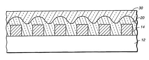
With reference to Fig. 2, a layer of high ozone
undoped silicon dioxide film 20 is deposited on top of
the semiconductor substrate 12 and the polysilicon
conductors 14. The high ozone undoped silicon dioxide
film covers the polysilicon conductors 14 and fills the
gaps 16 between the polysilicon conductors 14. The
thickness of the first film layer 20 is not less than
100nm but not greater than 400nm. The ozone
concentration of the first film layer 20 is not less than
120 g/m3 but not greater than 140 g/m3. This first layer
of film 20 is not doped with boron or phosphorus so as to
give the best possible as deposited gapfill behavior.
One feature in the first film layer 20 is the high
ozone/TEOS volume ratio of the film. In the prior art,
it has been common to use films having a ozone/TEOS ratio
of approximately 10 to 1. In the present invention, the
ratio of ozone/TEOS is above 15 to l, and preferably
about 17 to 1. The higher ozone/TEOS ratio promotes the
formation of dimers, which is a combination of two
monomers, which have high surface mobility. The high
surface mobility forms a complete surface reaction, not
just a gas phase reaction. Because a complete surface
reaction is formed, the ions are mobile on the surface
and find the location of the least amount of energy.
This causes the surface mobility to be high and the film
to have a flow-like characteristic. Because the
reactants can diffuse readily on the surface, the film
fills high aspect ratio gaps between the polysilicon
conductors fully and completely without leaving any voids
or seams.
CA 02417236 2003-02-03
WO 02/19411 PCT/USO1/22855
_7_
With reference to Fig. 3, a layer of low ozone
doped BPSG film 30 is deposited over the silicon dioxide
film 20. The thickness of the second film layer 30 is
not less than 500nm. It is important that the BPSG film
be thick enough so that after subsequent planarization,
there is sufficient thickness of BPSG film over the
entire device. An optimum thickness of BPSG film after
planarization would be at least 200nm. Thus, generally
the thickness of the dielectric film would be comprised
of no more than about 30 percent of the first film layer,
undoped silicon dioxide, 20 and at least 70 percent of
the second film layer, BPSG film 30. The ozone
concentration of the BPSG film 30 is not less than 70 g/m3
but not greater than 100 g/m3. The boron weight
percentage in the BPSG film typically ranges from 0 to 4
percent and the phosphorus weight percentage of this film
does not exceed 6 percent and typically ranges from 4 to
6 percent. The BPSG film 30 provides the mobile ion
Bettering function that is required by the semiconductor
device.
Then the substrate 12 having the two layers 20
and 30 formed on the top undergoes a heat treatment at a
temperature not exceeding 850°C. Ideally, the
temperature of the heat treatment would be approximately
700°C in order to be high enough to provide adequate
reflow, but low enough to not affect the device
characteristics when the device has a smaller device
geometry. As discussed above, since the dielectric film,
consisting of the layer of silicon dioxide 20 and the
layer of BPSG 30, has good as-deposited gapfill
characteristics, the film does not need to annealed at a
high temperature. The annealing is done to density the
film, rather than to soften and flow the film. In the
present invention, the annealing is done at a temperature
between 700°C and 800°C to obtain a sufficiently dense
pre-metal dielectric film necessary for manufacturable
contact etch profile and etch rate.
CA 02417236 2003-02-03
WO 02/19411 PCT/USO1/22855
_g_
With reference to Fig. 4, the top dielectric
film layer 30 is planarized using any of the known
planarization techniques, including chemical mechanical
planarization. As discussed above, the top BPSG layer
should be at least 200nm thick after planarization to
allow for adequate mobile-ion Bettering. The finished
silicon substrate is now ready for the metallization
process, in which metal is deposited through the
dielectric layer to form metal wiring conductors which
interconnect the components formed in the silicon
substrate to achieve the desired circuit on the
integrated circuit chip. The use of the above-described
method of forming a dielectric film layer is not limited
to use on semiconductor film layer is not limited to use
on semiconductor substrates, but could also be used in
forming an insulation layer over two or more polysilicon
buses formed on a substrate or in providing an insulating
layer in any circumstances in which it is critical for
the insulation layer to have good gapfill qualities.